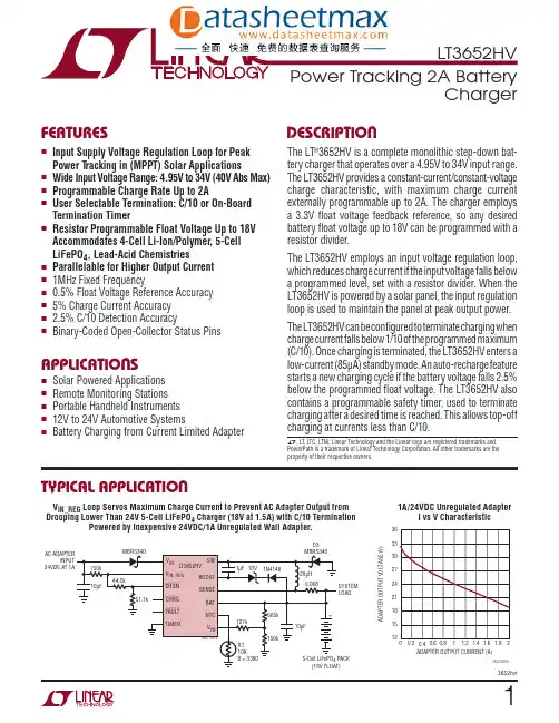
13652hvfT YPICAL APPLICATIOND ESCRIPTION ChargerThe LT ®3652HV is a complete monolithic step-down bat-tery charger that operates over a 4.95V to 34V input range. The LT3652HV provides a constant-current/constant-voltage charge characteristic, with maximum charge current externally programmable up to 2A. The charger employs a 3.3V fl oat voltage feedback reference, so any desired battery fl oat voltage up to 18V can be programmed with a resistor divider.The LT3652HV employs an input voltage regulation loop, which reduces charge current if the input voltage falls below a programmed level, set with a resistor divider. When the LT3652HV is powered by a solar panel, the input regulation loop is used to maintain the panel at peak output power.The L T3652HV c an b e c onfi gured t o t erminate c harging w hen charge c urrent f alls b elow 1/10 o f t he p rogrammed m aximum (C/10). Once charging is terminated, the LT3652HV enters a low-current (85μA) standby mode. An auto-recharge feature starts a new charging cycle if the battery voltage falls 2.5% below the programmed fl oat voltage. The LT3652HV also contains a programmable safety timer, used to terminate charging after a desired time is reached. This allows top-off charging at currents less than C/10.F EATURESA PPLICATIONS nInput Supply Voltage Regulation Loop for Peak Power T racking in (MPPT) Solar Applicationsn Wide Input Voltage Range: 4.95V to 34V (40V Abs Max)n Programmable Charge Rate Up to 2An User Selectable Termination: C/10 or On-Board Termination Timern Resistor Programmable Float Voltage Up to 18V Accommodates 4-Cell Li-Ion/Polymer , 5-Cell LiFePO 4, Lead-Acid Chemistriesn Parallelable for Higher Output Current n 1MHz Fixed Frequencyn 0.5% Float Voltage Reference Accuracy n 5% Charge Current Accuracy n 2.5% C/10 Detection Accuracyn Binary-Coded Open-Collector Status PinsnSolar Powered Applications n Remote Monitoring Stations n Portable Handheld Instruments n 12V to 24V Automotive SystemsnBattery Charging from Current Limited AdapterL , L T , L TC, L TM, Linear Technology and the Linear logo are registered trademarks and PowerPath is a trademark of Linear Technology Corporation. All other trademarks are the property of their respective owners.V IN_REG Loop Servos Maximum Charge Current to Prevent AC Adapter Output from Drooping Lower Than 24V 5-Cell LiFePO 4 Charger (18V at 1.5A) with C/10 TerminationPowered by Inexpensive 24VDC/1A Unregulated Wall Adapter.SYSTEM LOADD3ADAPTER OUTPUT CURRENT (A)00.2A D A P T E R O U T P U T V O L T A G E (V )12151833302724210.61 1.23652 TA01b360.40.8 1.61.421.81A/24VDC Unregulated AdapterI vs V CharacteristicLT3652HV23652hvfP IN CONFIGURATIONA BSOLUTE MAXIMUM RATINGS Voltages:V IN ........................................................................40V V IN_REG , SHDN , CHRG , FAUL T ............V IN + 0.5V , 40V SW ........................................................................40V SW-V IN .................................................................4.5V BOOST ...................................................SW+10V , 50V BAT , SENSE .. (20V)(Note 1)ORDER INFORMATIONLEAD FREE FINISH TAPE AND REEL PART MARKING*PACKAGE DESCRIPTION TEMPERATURE RANGE LT3652HVEDD#PBF LT3652HVEDD#TRPBF LFRG 12-Lead Plastic DFN 3mm × 3mm –40°C to 125°C LT3652HVIDD#PBF LT3652HVIDD#TRPBF LFRG 12-Lead Plastic DFN 3mm × 3mm –40°C to 125°C LT3652HVEMSE#PBF LT3652HVEMSE#TRPBF 3652HV 12-Lead Plastic MSOP –40°C to 125°C LT3652HVIMSE#PBFLT3652HVIMSE#TRPBF3652HV12-Lead Plastic MSOP–40°C to 125°CConsult LTC Marketing for parts specifi ed with wider operating temperature ranges. *The temperature grade is identifi ed by a label on the shipping container.Consult LTC Marketing for information on non-standard lead based fi nish parts.For more information on lead free part marking, go to: /leadfree/ For more information on tape and reel specifi cations, go to: /tapeandreel/TOP VIEWDD PACKAGE12-LEAD (3mm × 3mm) PLASTIC DFN1211891045321SW BOOST SENSE BAT NTCV FBV IN V IN_REG SHDN CHRG FAUL T TIMER6713123456V IN V IN_REG SHDN CHRG FAUL T TIMER 121110987SW BOOST SENSE BAT NTC V FBTOP VIEW13MSE PACKAGE12-LEAD PLASTIC MSOPT JMAX = 125°C, θJA = 43°C/W , θJC = 3°C/WEXPOSED PAD (PIN 13) IS GND, MUST BE SOLDERED TO PCBT JMAX = 125°C, θJA = 43°C/W , θJC = 3°C/WEXPOSED PAD (PIN 13) IS GND, MUST BE SOLDERED TO PCBBAT-SENSE .........................................–0.5V to +0.5VNTC, TIMER, ........................................................2.5V V FB ..........................................................................5V Operating Junction Temperature Range(Note 2) .............................................–40°C to 125°C Storage Temperature Range ...................–65°C to 150°CLT3652HV33652hvfE LECTRICAL CHARACTERISTICSSYMBOL PARAMETER CONDITIONS MIN TYP MAX UNITSV IN V IN Operating RangeV IN Start Voltage V BAT = 4.2 (Notes 3, 4)V BAT = 4.2 (Note 4)l l 4.957.534V V V IN(OVLO)OVLO Threshold OVLO Hysteresis V IN Rising l3435140V V V IN(UVLO)UVLO Threshold UVLO Hysteresis V IN Rising 4.60.24.95V V V FB(FL T)Float Voltage Reference (Note 6)l 3.2823.263.3 3.3183.34V V ΔV RECHARGE Recharge Reference Threshold Voltage Relative to V FB(FL T) (Note 6)82.5mV V FB(PRE)Reference Precondition Threshold V FB Rising (Note 6)2.3V V FB(PREHYST)Reference Precondition Threshold HysteresisVoltage Relative to V FB(PRE) (Note 6)70mVV IN_REG(TH)Input Regulation Reference V FB = 3V; V SENSE – V BAT = 50mV l 2.65 2.7 2.75V I IN_REG Input Regulation Reference Bias Current V IN_REG = V IN_REG(TH)l 35100nA I VINOperating Input Supply CurrentCC/CV Mode, I SW = 0Standby ModeShutdown (SHDN = 0)l 2.58515 3.5mA μA μA I BOOST BOOST Supply Current Switch On, I SW = 0,2.5 < V (BOOST – SW) < 8.520mA I BOOST/I SW BOOST Switch Drive I SW = 2A30mA/A V SW(ON)Switch-On Voltage Drop V IN – V SW , I SW = 2A350mV I SW(MAX)Switch Current Limit l 2.53A V SENSE(PRE)Precondition Sense Voltage V SENSE – V BAT ; V FB = 2V 15mVV SENSE(DC)Maximum Sense Voltage V SENSE – V BAT ; V FB = 3V (Note 7)l 95100105mV V SENSE(C/10)C/10 T rigger Sense Voltage V SENSE – V BAT , Falling l7.51012.5mV I BAT BAT Input Bias Current Charging Terminated 0.11μA I SENSE SENSE Input Bias Current Charging Terminated 0.11μA I VFB V FB Input Bias Current Charging Terminated 65nA I VFB V FB Input Bias Current CV Operation (Note 5)110nAV NTC(H)NTC Range Limit (High)V NTC Rising l 1.25 1.36 1.45V V NTC(L)NTC Range Limit (Low)V NTC Falling l 0.270.290.315V V NTC(HYST)NTC Threshold Hysteresis % of threshold 20%R NTC(DIS)NTC Disable Impedance Impedance to ground l 250500kΩI NTC NTC Bias Current V NTC = 0.8V l 47.55052.5μA V SHDN Shutdown Threshold Risingl 1.151.2 1.25V V SHDN (HYST)Shutdown Hysteresis 120mV I SHDN SHDN Input Bias Current –10nAV CHRG , V FAUL T Status Low Voltage 10mA Load l 0.4V I TIMER Charge/Discharge Current 25μA V TIMER(DIS)Timer Disable Thresholdl0.10.25VThe l denotes the specifi cations which apply over the full operating junction temperature range, otherwise specifi cations are at T A = 25°C. V IN = 20V, Boost – SW = 4V, SHDN = 2V, V FB = 3.3V, C TIMER= 0.68μF.LT3652HV43652hvfSYMBOL PARAMETERCONDITIONS MIN TYP MAX UNITSt TIMERFull Charge Cycle Timeout 3hr Precondition Timeout 22.5minTimer Accuracyl–1010%f O Operating Frequency 1MHz DCDuty Cycle RangeContinuous Operationl 1590%E LECTRICAL CHARACTERISTICS The l denotes the specifi cations which apply over the full operating junction temperature range, otherwise specifi cations are at T A = 25°C. V IN = 20V, Boost – SW = 4V, SHDN = 2V, V FB = 3.3V, C TIMER = 0.68μF.Note 1: Stresses beyond those listed under Absolute Maximum Ratings may cause permanent damage to the device. Exposure to any Absolute Maximum Rating condition for extended periods may affect device reliability and lifetime.Note 2: The L T3652HV is tested under pulsed load conditions such that T J ≅ T A . The L T3652HVE is guaranteed to meet performance specifi cations from 0°C to 85°C junction temperature. Specifi cations over the –40°C to 125°C operating junction temperature range are assured by design, characterization, and correlation with statistical process controls. The L T3652HVI specifi cations are guaranteed over the full –40°C to 125°C operating junction temperature range. High junction temperatures degrade operating lifetimes; operating lifetime is derated for junction temperatures greater than 125°C.Note 3: V IN minimum voltages below the start threshold are only supported if (V BOOST -V SW ) > 2V .Note 4: This parameter is valid for programmed output battery fl oat voltages ≤ 4.2V . V IN operating range minimum is 0.75V above the programmed output battery fl oat voltage (V BAT(FL T) + 0.75V). V IN Start Voltage is 3.3V above the programmed output battery fl oat voltage (V BAT(FL T) + 3.3V).Note 5: Output battery fl oat voltage (V BAT(FL T)) programming resistor divider equivalent resistance = 250k compensates for input bias current. Note 6: All V FB voltages measured through 250k series resistance.Note 7: V SENSE(DC) is reduced by thermal foldback as junction temperature approaches 125°C.LT3652HV53652hvfT YPICAL PERFORMANCE CHARACTERISTICS Switch Forward Drop (V IN – V SW ) vs TemperatureCC/CV Charging; SENSE Pin Bias Current vs V SENSEC/10 Threshold (V SENSE –V BAT ) vs TemperatureV FB Reference Voltage vs TemperatureV IN Standby Mode Current vs TemperatureSwitch Drive (I SW /I BOOST ) vs Switch CurrentT J = 25°C, unless otherwise noted.TEMPERATURE (°C)–50V F B (F L T )3.2963.2983.3003.302050753652 G01a3.304–2525100125TEMPERATURE (°C)–5065I V I N C U R R E N T (μA )70758010090050753652 G029585–2525100SWITCH CURRENT (A)I S W /I B O O S T18243036 1.6126021273315930.40.8 1.20.2 1.80.6 1.0 1.4 2.03652 G03TEMPERATURE (°C)–50320V S W (O N ) (m V )340360380480420050753652 G04440460400–2525100125V SENSE (V)–350I S E N S E (μA )–250–150–5010050–300–200–10003652 G05TEMPERATURE (°C)–508V S E N S E (C /10) (m V )9101112050753652 G06–2525100125TEMPERATURE (°C)–50V I N _R E G (T H ) (V )2.6802.6852.6902.7152.7102.7052.7002.695050753652 G012.720–2525100125V IN_REG Thresholdvs Temperature: I CHG at 50%LT3652HV63652hvfTYPICAL PERFORMANCE CHARACTERISTICSMaximum Charge Current (V SENSE –V BAT ) vs TemperatureThermal Foldback – Maximum Charge Current (V SENSE –V BAT ) vs TemperatureCC/CV Charging; BAT Pin Bias Current vs V BATT A = 25°C, unless otherwise noted.TEMPERATURE (°C)–5099.0V S E N S E (D C ) (m V )99.299.699.8100.0101.0100.4050753652 G0799.4100.6100.8100.2–2525100125TEMPERATURE (°C)V S E N S E (D C )(m V )4080206010012045658510512535135255575951153652 G08V BAT (V)–0.4I B A T (m A )0.00.40.82.21.62.01.2–0.20.20.61.01.81.43652 G09V IN_REG (V)2.65V S E N S E (D C ) (m V )208060402.67 2.692.73652 G101002.66 2.682.722.71 2.732.742.75V BAT(FL T) (V)020I R F B (μA )861012183652 G114264810121614TIME (MINUTES)EFFICIENCY (%)C H A R G E C U R R E N T (A ); P OW E R L O S S (W )0.52.02.51.51.040801003652 G123.0354575655595852060140120160180200Maximum Charge Current(V SENSE –V BAT ) vs V IN_REG VoltageV FLOAT Programming Resistor Current vs V FLOAT for 2-Resistor NetworkCharge Current, Effi ciency, and Power Loss vs Time(I CHG(MAX) = 2A; V FLOAT = 8.2V)Charger Effi ciency vs Battery Voltage (I CHG= 2A)V BAT (V)70E F F I C I E N C Y (%)7680828486887472789057911134141536810123652 G13LT3652HV73652hvfP IN FUNCTIONS V IN (Pin 1): Charger Input Supply. V IN operating range is 4.95V to 34V. V IN must be 3.3V greater than the pro-grammed output battery fl oat voltage (V BAT(FLT)) for reli-able start-up. (V IN – V BAT(FLT)) ≥ 0.75V is the minimum operating voltage, provided (V BOOST – V SW ) ≥ 2V. I VIN ~ 85μA after charge termination. This pin is typically con-nected to the cathode of a blocking diode.V IN_REG (Pin 2): Input Voltage Regulation Reference. Maxi-mum charge current is reduced when this pin is below 2.7V. Connecting a resistor divider from V IN to this pin enables programming of minimum operational V IN voltage. This is typically used to program the peak power voltage for a solar panel. The LT3652HV servos the maximum charge current required to maintain the programmed operational V IN voltage, through maintaining the voltage on V IN_REG at or above 2.7V. If the voltage regulation feature is not used, connect the pin to V IN .SHDN (Pin 3): Precision Threshold Shutdown Pin. The enable threshold is 1.2V (rising), with 120mV of input hysteresis. When in shutdown mode, all charging functions are disabled. The precision threshold allows use of the SHDN pin to incorporate UVLO functions. If the SHDN pin is pulled below 0.4V, the IC enters a low current shutdown mode where V IN current is reduced to 15μA. Typical SHDN pin input bias current is 10nA. If the shutdown function is not desired, connect the pin to V IN .CHRG (Pin 4): Open-Collector Charger Status Output; typically pulled up through a resistor to a reference volt-age. This status pin can be pulled up to voltages as high as V IN when disabled, and can sink currents up to 10mA when enabled. During a battery charging cycle, if required charge current is greater than 1/10 of the programmed maximum current (C/10), CHRG is pulled low. A tem-perature fault also causes this pin to be pulled low. After C/10 charge termination or, if the internal timer is used for termination and charge current is less than C/10, the CHRG pin remains high-impedance.FAULT (Pin 5): Open-Collector Charger Status Output; typically pulled up through a resistor to a reference volt-age. This status pin can be pulled up to voltages as high as V IN when disabled, and can sink currents up to 10mA when enabled. This pin indicates fault conditions during abattery charging cycle. A temperature fault causes this pin to be pulled low. If the internal timer is used for termina-tion, a bad battery fault also causes this pin to be pulled low. If no fault conditions exist, the FAULT pin remains high-impedance.TIMER (Pin 6): End-Of-Cycle Timer Programming Pin. If a timer-based charge termination is desired, connect a capacitor from this pin to ground. Full charge end-of-cycle time (in hours) is programmed with this capacitor following the equation: t EOC = C TIMER • 4.4 • 106A bad battery fault is generated if the battery does not achieve the precondition threshold voltage within one-eighth of t EOC , or: t PRE = C TIMER • 5.5 • 105A 0.68μF capacitor is typically used, which generates a timer EOC at three hours, and a precondition limit time of 22.5 minutes. If a timer-based termination is not desired, the timer function is disabled by connecting the TIMER pin to ground. With the timer function disabled, charging terminates when the charge current drops below a C/10 threshold, or I CHG(MAX)/10V FB (Pin 7): Battery Float Voltage Feedback Reference. The charge function operates to achieve a fi nal fl oat voltage of 3.3V on this pin. Output battery fl oat voltage (V BAT(FLT)) is programmed using a resistor divider. V BAT(FLT) can be programmed up to 18V.The auto-restart feature initiates a new charging cyclewhen the voltage at the V FB pin falls 2.5% below the float voltage reference.The V FB pin input bias current is 110nA. Using a resistor divider with an equivalent input resistance at the V FB pin of 250k compensates for input bias current error.Required resistor values to program desired V BAT(FLT) follow the equations:R1 = (V BAT(FLT) • 2.5 • 105)/3.3 (Ω) R2 = (R1 • 2.5 • 105)/(R1 - (2.5 • 105))(Ω)R1 is connected from BAT to V FB , and R2 is connected from V FBto ground.LT3652HV 83652hvfNTC (Pin 8): Battery Temperature Monitor Pin. This pin is the input to the NTC (Negative Temperature Coeffi cient) thermistor temperature monitoring circuit. This function is enabled by connecting a 10kΩ, B = 3380 NTC thermistor from the NTC pin to ground. The pin sources 50μA, and monitors the voltage across the 10kΩ thermistor. When the voltage on this pin is above 1.36 (T < 0°C) or below 0.29V (T > 40°C), charging is disabled and the CHRG and FAULT pins are both pulled low. If internal timer termina-tion is being used, the timer is paused, suspending the charging cycle. Charging resumes when the voltage on NTC returns to within the 0.29V to 1.36V active region. There is approximately 5°C of temperature hysteresis associated with each of the temperature thresholds. The temperature monitoring function remains enabled while the thermistor resistance to ground is less than 250k, so if this function is not desired, leave the NTC pin unconnected.BAT (Pin 9): Charger Output Monitor Pin. Connect a 10μF decoupling capacitance (C BAT ) to ground. Depend-ing on application requirements, larger value decoupling capacitors may be required. The charge function operates to achieve the programmed output battery fl oat voltage (V BAT(FLT)) at this pin. This pin is also the reference for the current sense voltage. Once a charge cycle is termi-nated, the input bias current of the BAT pin is reduced to < 0.1μA, to minimize battery discharge while the charger remains connected.SENSE (Pin 10): Charge Current Sense Pin. Connect the inductor sense resistor (R SENSE ) from the SENSE pin to the BAT pin. The voltage across this resistor sets the averagecharge current. The maximum charge current (I CHG(MAX)) corresponds to 100mV across the sense resistor. This resistor can be set to program maximum charge cur-rent as high as 2A. The sense resistor value follows the relation:R SENSE = 0.1/I CHG(MAX) (Ω)Once a charge cycle is terminated, the input bias current of the SENSE pin is reduced to < 0.1μA, to minimize battery discharge while the charger remains connected.BOOST (Pin 11): Bootstrapped Supply Rail for Switch D rive. This pin facilitates saturation of the switch transistor. Connect a 1μF or greater capacitor from the BOOST pin to the SW pin. Operating range of this pin is 0V to 8.5V, referenced to the SW pin. The voltage on the decoupling capacitor is refreshed through a rectifying diode, with the anode connected to either the battery output voltage or an external source, and the cathode connected to the BOOST pin.SW (Pin 12): Switch Output Pin. This pin is the output of the charger switch, and corresponds to the emitter of the switch transistor. When enabled, the switch shorts the SW pin to the V IN supply. The drive circuitry for this switch is bootstrapped above the V IN supply using the BOOST supply pin, allowing saturation of the switch for maximum effi ciency. The effective on-resistance of the boosted switch is 0.175Ω.SGND (Pin 13): Ground Reference and Backside Exposed Lead Frame Thermal Connection. Solder the exposed lead frame to the PCB ground plane.P IN FUNCTIONSLT3652HV93652hvfB LOCK DIAGRAM+–LT3652HV103652hvfA PPLICATIONS INFORMATION OverviewL T3652HV is a complete monolithic, mid-power , multi-chemistry buck battery charger , addressing high input voltage applications with solutions that require a minimum of external components. The IC uses a 1MHz constant fre-quency, average-current mode step-down architecture.The L T3652HV incorporates a 2A switch that is driven by a bootstrapped supply to maximize efficiency during charging cycles. Wide input range allows operation to full charge from voltages as high as 34V . A precision threshold shutdown pin allows incorporation of UVLO functionality using a simple resistor divider . The IC can also be put into a low-current shutdown mode, in which the input supply bias is reduced to only 15μA.The L T3652HV employs an input voltage regulation loop, which reduces charge current if a monitored input voltage falls below a programmed level. When the L T3652HV is powered by a solar panel, the input regulation loop is used to maintain the panel at peak output power .The L T3652HV automatically enters a battery precondition mode if the sensed battery voltage is very low. In this mode, the charge current is reduced to 15% of the programmed maximum, as set by the inductor sense resistor , R SENSE . Once the battery voltage reaches 70% of the fully charged float voltage, the IC automatically increases maximum charge current to the full programmed value.The L T3652HV can use a charge-current based C/10 termination scheme, which ends a charge cycle when the battery charge current falls to one tenth of the pro-grammed maximum charge current. The L T3652HV also contains an internal charge cycle control timer , for timer-based termination. When using the internal timer , the IC combines C/10 detection with a programmable time constraint, during which the charging cycle can continue beyond the C/10 level to top-off a battery. The charge cycle terminates when a specific time elapses, typically 3 hours. When the timer-based scheme is used, the IC also supports bad battery detection, which triggers a system fault if a battery stays in precondition mode for more than one eighth of the total charge cycle time.Once charging is terminated, the L T3652HV automati-cally enters a low-current standby mode where supply bias currents are reduced to 85μA. The IC continues tomonitor the battery voltage while in standby, and if that voltage falls 2.5% from the full-charge float voltage, the L T3652HV engages an automatic charge cycle restart. The IC also automatically restarts a new charge cycle after a bad battery fault once the failed battery is removed and replaced with another battery.The L T3652HV contains provisions for a battery tem-perature monitoring circuit. This feature monitors battery temperature using a thermistor during the charging cycle. If the battery temperature moves outside a safe charg-ing range of 0°C to 40°C, the IC suspends charging and signals a fault condition until the temperature returns to the safe charging range.The L T3652HV contains two digital open-collector outputs, which provide charger status and signal fault conditions. These binary-coded pins signal battery charging, standby or shutdown modes, battery temperature faults, and bad battery faults.General Operation (See Block Diagram)The L T3652HV uses average current mode control loop architecture, such that the IC servos directly to average charge current. The L T3652HV senses charger output voltage through a resistor divider via the V FB pin. The difference between the voltage on this pin and an internal 3.3V voltage reference is integrated by the voltage error amplifier (V-EA). This amplifier generates an error volt-age on its output (I TH ), which corresponds to the average current sensed across the inductor current sense resistor , R SENSE , which is connected between the SENSE and BAT pins. The I TH voltage is then divided down by a factor of 10, and imposed on the input of the current error amplifier (C-EA). The difference between this imposed voltage and the current sense resistor voltage is integrated, with the resulting voltage (V C ) used as a threshold that is compared against an internally generated ramp. The output of this comparison controls the charger’s switch.The I TH error voltage corresponds linearly to average current sensed across the inductor current sense resistor , allowing maximum charge current control by limiting the effective voltage range of I TH . A clamp limits this voltage to 1V which, in turn, limits the current sense voltage to 100mV . This sets the maximum charge current, or the current delivered while the charger is operating in con-A PPLICATIONS INFORMATIONstant-current (CC) mode, which corresponds to 100mV across R SENSE. The I TH voltage is pulled down to reduce this maximum charge current should the voltage on the V IN_REG pin falls below 2.7V (V IN_REG(TH)) or the die tem-perature approaches 125°C.If the voltage on the V FB pin is below 2.3V (V FB(PRE)), the L T3652HV engages precondition mode. D uring the precondition interval, the charger continues to operate in constant-current mode, but the maximum charge current is reduced to 15% of the maximum programmed value as set by R SENSE.When the charger output voltage approaches the float volt-age, or the voltage on the V FB pin approaches 3.3V (V FB(FL T)), the charger transitions into constant-voltage (CV) mode and charge current is reduced from the maximum value. As this occurs, the I TH voltage falls from the limit clamp and servos to lower voltages. The IC monitors the I TH volt-age as it is reduced, and detection of C/10 charge current is achieved when I TH = 0.1V. If the charger is configured for C/10 termination, this threshold is used to terminate the charge cycle. Once the charge cycle is terminated, the CHRG status pin becomes high-impedance and the charger enters low-current standby mode.The L T3652HV contains an internal charge cycle timer that terminates a successful charge cycle after a programmed amount of time. This timer is typically programmed to achieve end-of-cycle (EOC) in 3 hours, but can be con-figured for any amount of time by setting an appropriate timing capacitor value (C TIMER). When timer termination is used, the charge cycle does not terminate when C/10 is achieved. Because the CHRG status pin responds to the C/10 current level, the IC will indicate a fully-charged battery status, but the charger continues to source low currents into the battery until the programmed EOC time has elapsed, at which time the charge cycle will terminate. At EOC when the charging cycle terminates, if the battery did not achieve at least 97.5% of the full float voltage, charging is deemed unsuccessful, the L T3652HV re-initiates, and charging continues for another full timer cycle.Use of the timer function also enables bad-battery detec-tion. This fault condition is achieved if the battery does not respond to preconditioning, such that the charger remains in (or enters) precondition mode after 1/8th of the programmed charge cycle time. A bad battery fault halts the charging cycle, the CHRG status pin goes high-impedance, and the FAUL T pin is pulled low.When the L T3652HV terminates a charging cycle, whether through C/10 detection or by reaching timer EOC, the average current mode analog loop remains active, but the internal float voltage reference is reduced by 2.5%. Because the voltage on a successfully charged battery is at the full float voltage, the voltage error amp detects an over-voltage condition and I TH is pulled low. When the voltage error amp output drops below 0.3V, the IC enters standby mode, where most of the internal circuitry is dis-abled, and the V IN bias current is reduced to 85μA. When the voltage on the V FB pin drops below the reduced float reference level, the output of the voltage error amp will climb, at which point the IC comes out of standby mode and a new charging cycle is initiated.V IN Input SupplyThe L T3652HV is biased through a reverse-current block-ing element from the charger input supply to the V IN pin. This supply provides large switched currents, so a high-quality, low ESR decoupling capacitor is recommended to minimize voltage glitches on V IN. The V IN decoupling capacitor (C VIN) absorbs all input switching ripple current in the charger, so it must have an adequate ripple current rating. RMS ripple current (I CVIN(RMS)) is:I CVIN(RMS)≅ I CHG(MAX) • (V BAT / V IN)•([V IN / V BAT] – 1)1/2,where I CHG(MAX) is the maximum average charge current (100mV/R SENSE). The above relation has a maximum at V IN = 2 • V BAT, where:I CVIN(RMS) = I CHG(MAX)/2.The simple worst-case of ½ • I CHG(MAX) is commonly used for design.。