Low Power Design of High Speed CMOS Pulse Stream Neuron Circuit
- 格式:pdf
- 大小:1.26 MB
- 文档页数:5

256K (32K x 8) Static RAMCY62256Features•High speed —55ns •Temperature Ranges —Commercial: 0°C to 70°C —Industrial: –40°C to 85°C —Automotive: –40°C to 125°C •Voltage range —4.5V – 5.5V•Low active power and standby power•Easy memory expansion with CE and OE features •TTL-compatible inputs and outputs •Automatic power-down when deselected •CMOS for optimum speed/power•Available in a Pb-free and non Pb-free standard 28-pin narrow SOIC, 28-pin TSOP-1, 28-pin Reverse TSOP-1 and 28-pin DIP packagesFunctional Description [1]The CY62256 is a high-performance CMOS static RAM organized as 32K words by 8 bits. Easy memory expansion is provided by an active LOW chip enable (CE) and active LOW output enable (OE) and Tri-state drivers. This device has an automatic power-down feature, reducing the power consumption by 99.9% when deselected.An active LOW write enable signal (WE) controls the writing/reading operation of the memory. When CE and WE inputs are both LOW, data on the eight data input/output pins (I/O 0 through I/O 7) is written into the memory location addressed by the address present on the address pins (A 0through A 14). Reading the device is accomplished by selecting the device and enabling the outputs, CE and OE active LOW,while WE remains inactive or HIGH. Under these conditions,the contents of the location addressed by the information on address pins are present on the eight data input/output pins.The input/output pins remain in a high-impedance state unless the chip is selected, outputs are enabled, and write enable (WE) is HIGH.Note:1.For best practice recommendations, please refer to the Cypress application note “System Design Guidelines” on .A 9A 8A 7A 6A 5A 4A 3A 2COLUMN DECODERR O W D E C O D E RS E N S E A M P SINPUTBUFFERPOWER DOWNWE OEI/O 0CE I/O 1I/O 2I/O 3I/O 7I/O 6I/O 5I/O 4A 10A 13A 11A 12A A 14A 1Logic Block Diagram32K × 8ARRAYPin ConfigurationsProduct PortfolioProductV CC Range (V)Speed (ns)Power DissipationOperating, I CC(mA)Standby, I SB2(µA)Min.Typ.[2]Max.Typ.[2]Max.Typ.[2]Max.CY62256L Com’l/Ind’l 4.55.05.555/702550250CY62256LL Commercial 7025500.15CY62256LL Industrial 55/7025500.110CY62256LLAutomotive5525500.11512345678910111415162019181721242322Top ViewNarrow SOIC 121325282726GNDA 6A 7A 8A 9A 10A 11A 12A 13WE V CC A 4A 3A 2A 1I/O 7I/O 6I/O 5I/O 4A 14A 5I/O 0I/O 1I/O 2CE OE A 0I/O 322232425262728125101115141312161918173420217689OEA 1A 2A 3A 4WE V CC A 5A 6A 7A 8A 9A 0CE I/O 7I/O 6I/O 5GND I/O 2I/O 1I/O 4I/O 0A 14A 10A 11A 13A 12I/O 3TSOP I Top View (not to scale)Reverse Pinout 22232425262728125101115141312161918173420217689OE A 1A 2A 3A 4WE V CC A 5A 6A 7A 8A 9A 0CE I/O 7I/O 6I/O 5GND I/O 2I/O 1I/O 4I/O 0A 14A 10A 11A 13A 12I/O 3TSOP I Top View (not to scale)12345678910111415162019181721242322Top ViewDIP 121325282726GNDA 6A 7A 8A 9A 10A 11A 12A 13WE V CC A 4A 3A 2A 1I/O 7I/O 6I/O 5I/O 4A 14A 5I/O 0I/O 1I/O 2CE OE A 0I/O 3Pin DefinitionsPin Number Type Description1–10, 21, 23–26Input A 0–A 14. Address Inputs11–13, 15–19, Input/Output I/O 0–/O 7. Data lines. Used as input or output lines depending on operation27Input/Control WE . When selected LOW, a WRITE is conducted. When selected HIGH, a READ is conducted20Input/Control CE . When LOW, selects the chip. When HIGH, deselects the chip22Input/ControlOE . Output Enable. Controls the direction of the I/O pins. When LOW, the I/O pins behave as outputs. When deasserted HIGH, I/O pins are Tri-stated, and act as input data pins14GroundGND . Ground for the device28Power Supply V CC . Power supply for the deviceNote:2.Typical specifications are the mean values measured over a large sample size across normal production process variations and are taken at nominal conditions (T A = 25°C, V CC ). Parameters are guaranteed by design and characterization, and not 100% tested.Maximum Ratings(Above which the useful life may be impaired. For user guide-lines, not tested.)Storage Temperature .................................–65°C to +150°C Ambient Temperature withPower Applied.............................................–55°C to +125°C Supply Voltage to Ground Potential(Pin 28 to Pin 14)..............................................–0.5V to +7V DC Voltage Applied to Outputsin High-Z State[3]....................................–0.5V to V CC + 0.5V DC Input Voltage[3]................................–0.5V to V CC + 0.5V Output Current into Outputs (LOW).............................20 mA Static Discharge Voltage.......................................... > 2001V (per MIL-STD-883, Method 3015)Latch-up Current.................................................... > 200 mA Operating RangeRange Ambient Temperature (T A)[4]V CC Commercial0°C to +70°C 5V± 10% Industrial–40°C to +85°C 5V± 10% Automotive–40°C to +125°C 5V± 10%Electrical Characteristics Over the Operating RangeParameter Description Test ConditionsCY62256−55CY62256−70Unit Min.Typ.[2]Max.Min.Typ.[2]Max.V OH Output HIGH Voltage V CC = Min., I OH = −1.0 mA 2.4 2.4V V OL Output LOW Voltage V CC = Min., I OL = 2.1 mA0.40.4VV IH Input HIGH Voltage 2.2V CC+0.5V 2.2V CC+0.5VVV IL Input LOW Voltage–0.50.8–0.50.8V I IX Input Leakage Current GND < V I < V CC–0.5+0.5–0.5+0.5µA I OZ Output Leakage Current GND < V O < V CC, Output Disabled–0.5+0.5–0.5+0.5µAI CC V CC Operating SupplyCurrent V CC = 5.5V,I OUT = 0 mA,f = f Max = 1/t RCL25502550mALL25502550I SB1Automatic CEPower-down Current—TTL Inputs V CC = 5.5V, CE > V IH,V IN > V IH or V IN < V IL,f = f MaxL0.40.60.40.6mALL0.30.50.30.5I SB2Automatic CEPower-down Current—CMOS Inputs V CC = 5.5V,CE > V CC− 0.3VV IN > V CC− 0.3V, orV IN < 0.3V, f = 0L250250µALL - Com’l0.150.15LL - Ind’l0.1100.110LL - Auto0.115Capacitance[5]Parameter Description Test Conditions Max.UnitC IN Input Capacitance T A = 25°C, f = 1 MHz, V CC = V CC(typ.)6pFC OUT Output Capacitance8pF Thermal Resistance[5]Parameter Description Test Conditions DIP SOIC TSOP RTSOP UnitΘJA Thermal Resistance(Junction to Ambient)Still Air, soldered on a 4.25 x 1.125 inch,2-layer printed circuit board75.6176.5693.8993.89°C/WΘJC Thermal Resistance(Junction to Case)43.1236.0724.6424.64°C/WNotes:3.V IL (min.)= −2.0V for pulse durations of less than 20 ns.4.T A is the “Instant-On” case temperature.5.Tested initially and after any design or process changes that may affect these parameters.AC Test Loads and WaveformsData Retention CharacteristicsParameter DescriptionConditions [6]Min.Typ.[2]Max.Unit V DR V CC for Data Retention 2.0V I CCDRData Retention CurrentL V CC = 2.0V , CE > V CC − 0.3V ,V IN > V CC − 0.3V , or V IN < 0.3V250µA LL - Com’l 0.15µA LL - Ind’l 0.110µA LL - Auto0.110µA t CDR [5]Chip Deselect to Data Retention Time 0ns t R [5]Operation Recovery Timet RCnsData Retention WaveformNote:6.No input may exceed V CC + 0.5V .3.0V 5V OUTPUTR1 1800ΩR2990Ω100pF INCLUDING JIG AND SCOPEGND90%10%90%10%<5ns<5ns5V OUTPUTR1 1800ΩR2990Ω5pFINCLUDING JIG AND SCOPE (a)(b)OUTPUT1.77VEquivalent to:THE VENIN EQUIVALENTALL INPUT PULSES 639ΩV CC(min)V CC(min)t CDRV DR >2V DATA RETENTION MODEt RCEV CCSwitching Characteristics Over the Operating Range[7]Parameter DescriptionCY62256−55CY62256−70Unit Min.Max.Min.Max.Read Cyclet RC Read Cycle Time5570nst AA Address to Data Valid5570nst OHA Data Hold from Address Change55nst ACE CE LOW to Data Valid5570nst DOE OE LOW to Data Valid2535nst LZOE OE LOW to Low-Z[8]55nst HZOE OE HIGH to High-Z[8, 9]2025nst LZCE CE LOW to Low-Z[8]55nst HZCE CE HIGH to High-Z[8, 9]2025nst PU CE LOW to Power-up00nst PD CE HIGH to Power-down5570ns Write Cycle[10, 11]t WC Write Cycle Time5570nst SCE CE LOW to Write End4560nst AW Address Set-up to Write End4560nst HA Address Hold from Write End00nst SA Address Set-up to Write Start00nst PWE WE Pulse Width4050nst SD Data Set-up to Write End2530nst HD Data Hold from Write End00nst HZWE WE LOW to High-Z[8, 9]2025nst LZWE WE HIGH to Low-Z[8]55ns Notes:7.Test conditions assume signal transition time of 5 ns or less, timing reference levels of 1.5V, input pulse levels of 0 to 3.0V, and output loading of the specifiedI OL/I OH and 100 pF load capacitance.8.At any given temperature and voltage condition, t HZCE is less than t LZCE, t HZOE is less than t LZOE, and t HZWE is less than t LZWE for any given device.9.t HZOE, t HZCE, and t HZWE are specified with C L = 5 pF as in (b) of AC Test Loads. Transition is measured ±500 mV from steady-state voltage.10.The internal Write time of the memory is defined by the overlap of CE LOW and WE LOW. Both signals must be LOW to initiate a Write and either signal canterminate a Write by going HIGH. The data input set-up and hold timing should be referenced to the rising edge of the signal that terminates the Write.11.The minimum Write cycle time for Write Cycle #3 (WE controlled, OE LOW) is the sum of t HZWE and t SD.Switching WaveformsRead Cycle No. 1 (Address Transition Controlled)[12, 13]Read Cycle No. 2 (OE Controlled)[13, 14]Write Cycle No. 1 (WE Controlled)[10, 15, 16]Notes:12.Device is continuously selected. OE, CE = V IL .13.WE is HIGH for Read cycle.14.Address valid prior to or coincident with CE transition LOW.15.Data I/O is high impedance if OE = V IH .16.If CE goes HIGH simultaneously with WE HIGH, the output remains in a high-impedance state. 17.During this period, the I/Os are in output state and input signals should not be applied.ADDRESSDATA OUTPREVIOUS DATA VALIDDATA VALIDt RCt AAt OHA50%50%DATA VALIDt RCt ACEt DOEt LZOEt LZCE t PUHIGH IMPEDANCEt HZOE t HZCEt PDIMPEDANCEICCISBHIGH DATA OUTOECEV CC SUPPLY CURRENTt HDt SDt PWEt SAt HAt AWt WCt HZOEDATA IN VALIDNOTE 17DATA I/OADDRESSCEWEOEWrite Cycle No. 2 (CE Controlled)[10, 15, 16]Write Cycle No. 3 (WE Controlled, OE LOW)[11, 16]Switching Waveforms (continued)t WCt AWt SAt HAt HDt SDt SCEDATA IN VALIDWEDATA I/OADDRESSCEt HD t SDt LZWEt SAt HAt AWt WCt HZWEDATA IN VALIDNOTE 17DATA I/OADDRESSWECETypical DC and AC Characteristics1.21.41.00.60.40.24.04.55.05.56.01.61.41.21.00.8−5525125−55251251.21.00.8N O R M A L I Z E D t A A120100806040200.01.02.03.04.0O U T P U T S O U R C E C U R R E N T (m A )SUPPLY VOLTAGE (V)NORMALIZED SUPPLY CURRENT vs.SUPPLY VOLTAGENORMALIZED ACCESS TIME vs.AMBIENT TEMPERATURE AMBIENT TEMPERATURE (°C)NORMALIZED SUPPLY CURRENT vs.AMBIENT TEMPERATUREAMBIENT TEMPERATURE (°C)OUTPUT VOLTAGE (V)OUTPUT SOURCE CURRENT vs.OUTPUT VOLTAGE 0.00.81.41.11.00.94.04.55.05.56.0N O R M A L I Z E D t A ASUPPLY VOLTAGE (V)NORMALIZED ACCESS TIME vs.SUPPLY VOLTAGE 120140*********0.01.02.03.04.0O U T P U T S I N K C U R R E N T (m A )080OUTPUT VOLTAGE (V)OUTPUT SINK CURRENT vs.OUTPUT VOLTAGE0.60.40.20.0N O R M A L I Z E D I C CN O R M A L I Z E D I C C , I S BI CCI CCV CC = 5.0VV CC = 5.0V T A = 25°CV CC = 5.0V T A = 25°CI SBT A = 25°C0.60.801.31.2V IN = 5.0V T A = 25°C1.4V CC = 5.0V V IN = 5.0V−55251052.52.01.5CURRENT vs.AMBIENT TEMPERATUREAMBIENT TEMPERATURE (°C)1.00.50.0–0.5I SB3.0STANDBY V CC = 5.0V V IN = 5.0VI S B 2 µATruth TableCE WE OE Inputs/Outputs ModePowerH X X High-Z Deselect/Power-down Standby (I SB )L H L Data Out Read Active (I CC )L L X Data In WriteActive (I CC )LHHHigh-ZOutput DisabledActive (I CC )Typical DC and AC Characteristics (continued)3.02.52.01.51.00.50.01.02.03.04.0N O R M A L I Z E D I P OSUPPLY VOLTAGE (V)TYPICAL POWER-ON CURRENT vs.SUPPLY VOLTAGE 30.025.020.015.010.05.00200400600800D E L T A t (n s )AA CAPACITANCE (pF)TYPICAL ACCESS TIME CHANGE vs.OUTPUT LOADING1.251.000.7510203040N O R M A L I Z E D I C CCYCLE FREQUENCY (MHz)0.05.00.010000.50V CC = 4.5V T A = 25°CV CC =5.0V T A = 2 5°C V IN = 0.5VNORMALIZED I CC vs. CYCLE TIMEOrdering InformationSpeed(ns)Ordering Code PackageDiagram Package TypeOperatingRange55CY62256LL−55SNI51-8509228-pin (300-mil Narrow Body) SNC Industrial CY62256LL−55SNXI28-pin (300-mil Narrow Body) SNC (Pb-free)CY62256LL−55ZXI51-8507128-pin TSOP I (Pb-free)CY62256LL−55SNE51-8509228-pin (300-mil Narrow Body) SNC AutomotiveCY62256LL−55SNXE28-pin (300-mil Narrow Body) SNC (Pb-free)CY62256LL−55ZE51-8507128-pin TSOP ICY62256LL−55ZXE28-pin TSOP I (Pb-free)CY62256LL−55ZRXE51-8507428-pin Reverse TSOP I (Pb-free)70CY62256LL−70PC51-8501728-pin (600-Mil) Molded DIP Commercial CY62256LL−70PXC28-pin (600-Mil) Molded DIP (Pb-free)CY62256L−70SNC51-8509228-pin (300-mil Narrow Body) SNCCY62256L−70SNXC28-pin (300-mil Narrow Body) SNC (Pb-free)CY62256LL−70SNC28-pin (300-mil Narrow Body) SNCCY62256LL−70SNXC28-pin (300-mil Narrow Body) SNC (Pb-free)CY62256LL−70ZC51-8507128-pin TSOP ICY62256LL−70ZXC28-pin TSOP I (Pb-free)CY62256L–70SNI51-8509228-pin (300-mil Narrow Body) SNC IndustrialCY62256L–70SNXI28-pin (300-mil Narrow Body) SNC (Pb-free)CY62256LL−70SNI28-pin (300-mil Narrow Body) SNCCY62256LL−70SNXI28-pin (300-mil Narrow Body) SNC (Pb-free)CY62256LL−70ZXI51-8507128-pin TSOP I (Pb-free)CY62256LL−70ZRI51-8507428-pin Reverse TSOP ICY62256LL−70ZRXI28-pin Reverse TSOP I (Pb-free)Please contact your local Cypress sales representative for availability of these partsPackage DiagramsPackage Diagrams (continued)28-pin Thin Small Outline Package Type 1 (8 x 13.4 mm) (51-85071)51-85071-*GDocument #: 38-05248 Rev. *F Page 13 of 14All product and company names mentioned in this document are the trademarks of their respective holders.Package Diagrams (continued)51-85074-*F28-pin Reverse Thin Small Outline Package Type 1 (8x13.4 mm) (51-85074)Document History PageDocument Title: CY62256, 256K (32K x 8) Static RAM Document Number: 38-05248REV.ECN NO.IssueDateOrig. ofChange Description of Change**11345403/06/02MGN Change from Spec number: 38-00455 to 38-05248Remove obsolete parts from ordering info, standardize format*A11522705/23/02GBI Changed SN Package Diagram*B11650609/04/02GBI Added footnote 1Corrected package description in Ordering Information table*C238448See ECN AJU Added Automotive product information*D344595See ECN SYT Added Pb-free packages on page# 10*E395936See ECN SYT Changed address of Cypress Semiconductor Corporation on Page# 1 from“3901 North First Street” to “198 Champion Court”Added CY62256L–70SNXI package in the Ordering Information on Page # 10 *F493277See ECN VKN Updated Ordering Information table。
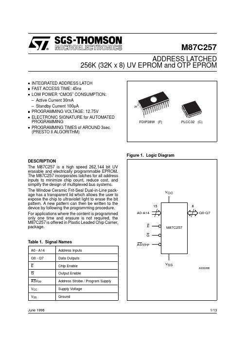
M87C257ADDRESS LATCHED256K (32K x 8) UV EPROM and OTP EPROMJune 19961/13Figure 1. Logic DiagramINTEGRATED ADDRESS LATCH FAST ACCESS TIME: 45nsLOW POWER “CMOS” CONSUMPTION:–Active Current 30mA –Standby Current 100µAPROGRAMMING VOLTAGE: 12.75VELECTRONIC SIGNATURE for AUTOMATED PROGRAMMINGPROGRAMMING TIMES of AROUND 3sec.(PRESTO II ALGORITHM)DESCRIPTIONThe M87C257 is a high speed 262,144 bit UV erasable and electrically programmable EPROM.The M87C257 incorporates latches for all address inputs to minimize chip count, reduce cost, and simplify the design of multiplexed bus systems.The Window Ceramic Frit-Seal Dual-in-Line pack-age has a transparent lid which allows the user to expose the chip to ultraviolet light to erase the bit pattern. A new pattern can then be written to the device by following the programming procedure.For applications where the content is programmed only one time and erasure is not required, the M87C257 is offered in Plastic Leaded Chip Carrier,package.Table 1. Signal NamesFigure 2A. DIP Pin ConnectionsFigure 2B. LCC Pin ConnectionsDEVICE OPERATIONThe modes of operation of the M87C257 are listed in the Operating Modes. A single power supply is required in the read mode. All inputs are TTL levels except for V PP and 12V on A9 for Electronic Signa-ture. Read ModeThe M87C257 has two control functions, both of which must be logically active in order to obtain data at the outputs. Chip Enable (E) is the power control and should be used for device selection.Output Enable (G) is the output control and shouldNotes:1.Except for the rating "Operating Temperature Range", stresses above those listed in the Table "Absolute Maximum Ratings"may cause permanent damage to the device. These are stress ratings only and operation of the device at these or any other conditions above those indicated in the Operating sections of this specification is not implied. Exposure to Absolute Maximum Rating conditions for extended periods may affect device reliability. Refer also to the SGS-THOMSON SURE Program and other relevant quality documents.2.Minimum DC voltage on Input or Output is –0.5V with possible undershoot to –2.0V for a period less than 20ns. Maximum DC voltage on Output is V CC +0.5V with possible overshoot to V CC +2V for a period less than 20ns.Table 2. Absolute Maximum Ratings (1)IH IL IDTable 3. Operating ModesTable 4. Electronic Signaturebe used to gate data to the output pins, inde-pendent of device selection. Assuming that the addresses are stable (AS = V IH ) or latched (AS =V IL ), the address access time (t AVQV ) is equal to the delay from E to output (t ELQV ). Data is available at the output after delay of t GLQV from the falling edge of G, assuming that E has been low and the ad-dresses have been stable for at least t AVQV -t GLQV .The M87C257 reduces the hardware interface in multiplexed address-data bus systems. The proc-essor multiplexed bus (AD0-AD7) may be tied to the M87C257’s address and data pins. No sepa-rate address latch is needed because the M87C257 latches all address inputs when AS is low.Standby ModeThe M87C257 has a standby mode which reduces the active current from 30mA to 100µA (Address Stable). The M87C257 is placed in the standby mode by applying a CMOS high signal to the E input. When in the standby mode, the outputs are in a high impedance state, independent of the G input.Two Line Output ControlBecause EPROMs are usually used in larger mem-ory arrays, this product features a 2 line control function which accommodates the use of multiple memory connection. The two line control function allows:a. the lowest possible memory power dissipation,b. complete assurance that output bus contention will not occur.For the most efficient use of these two control lines,E should be decoded and used as the primary device selecting function, while G should be made a common connection to all devices in the arraycontrol bus. This ensures that all deselected mem-ory devices are in their low power standby mode and that the output pins are only active when data is desired from a particular memory device.Figure 3. AC Testing Input Output WaveformFigure 4. AC Testing Load CircuitTable 5. AC Measurement ConditionsTable 6. Capacitance (1) (T A = 25 °C, f = 1 MHz )System ConsiderationsThe power switching characteristics of Advance CMOS EPROMs require careful decoupling of the devices. The supply current, I CC , has three seg-ments that are of interest to the system designer:the standby current level, the active current level,and transient current peaks that are produced by the falling and rising edges of E. The magnitude of this transient current peaks is dependent on the capacitive and inductive loading of the device at the output. The associated transient voltage peaks canbe suppressed by complying with the two lineoutput control and by properly selected decoupling capacitors. It is recommended that a 0.1µF ceramic capacitor be used on every device between V CC and V SS . This should be a high frequency capacitor of low inherent inductance and should be placed as close to the device as possible. In addition, a 4.7µF bulk electrolytic capacitor should be used between V CC and V SS for every eight devices. The bulk capacitor should be located near the power supply connection point. The purpose of the bulk capacitor is to overcome the voltage drop caused by the inductive effects of PCB traces.Notes:1.V CC must be applied simultaneously with or before V PP and removed simultaneously or after V PP .2.Maximum DC voltage on Output is V CC +0.5V.Table 7. Read Mode DC Characteristics (1)(T A = 0 to 70°C, –40 to 85°C, –40 to 105°C or –40 to 125°C; V CC = 5V ± 5% or 5V ± 10%; V PP = V CC )CC PP PP 2. Sampled only, not 100% tested.3.In case of 45ns speed see High Speed AC measurement conditions.Table 8A. Read Mode AC Characteristics (1)(T A = 0 to 70°C, –40 to 85°C, –40 to 105°C or –40 to 125°C; V CC = 5V ± 5% or 5V ± 10%; V PP = V CC )Notes:1. V CC must be applied simultaneously with or before V PP and removed simultaneously or after V PP .2. Sampled only, not 100% tested.Table 8B. Read Mode AC Characteristics (1)(T A = 0 to 70°C, –40 to 85°C, –40 to 105°C or –40 to 125°C; V CC = 5V ± 5% or 5V ± 10%; V PP = V CC )Figure 5. Read Mode AC WaveformsNote: 1.V CC must be applied simultaneously with or before V PP and removed simultaneously or after V PP .Table 9. Programming Mode DC Characteristics (1)(T A = 25 °C; V CC = 6.25V ± 0.25V; V PP = 12.75V ±0.25V)CC PP PPTable 10. Programming Mode AC Characteristics (1)(T A = 25 °C; V CC = 6.25V ± 0.25V; V PP= 12.75V ± 0.25V)ProgrammingWhen delivered (and after each erasure for UV EPROM), all bits of the M87C257 are in the "1"state. Data is introduced by selectively program-ming "0"s into the desired bit locations. Although only "0"s will be programmed, both "1"s and "0"s can be present in the data word. The only way tochange a "0" to a "1" is by die exposition to ultra-violet light (UV EPROM). The M87C257 is in the programming mode when V PP input is at 12.75V, G is at V IH and E is pulsed to V IL . The data to be programmed is applied to 8 bits in parallel to the data output pins. The levels required for the ad-dress and data inputs are TTL. V CC is specified to be 6.25 V ± 0.25 V.Figure 6. Programming and Verify Modes AC WaveformsPRESTO II Programming AlgorithmPRESTO II Programming Algorithm allows to pro-gram the whole array with a guaranteed margin, in a typical time of 3.5 seconds. Programming with PRESTO II involves the application of a sequence of 100µs program pulses to each byte until a correct verify occurs (see Figure 7). During programming and verify operation, a MARGIN MODE circuit is automatically activated in order to guarantee that each cell is programmed with enough margin. No overprogram pulse is applied since the verify in MARGIN MODE provides necessary margin to each programmed cell. Program InhibitProgramming of multiple M87C257s in parallel with different data is also easily accomplished. Except for E, all like inputs including G of the parallel M87C257 may be common. A TTL low level pulse applied to a M87C257’s E input, with V PP at 12.75V,will program that M87C257. A high level E inputinhibits the other M87C257s from being pro-grammed.Program VerifyA verify (read) should be performed on the pro-grammed bits to determine that they were correctlyprogrammed. The verify is accomplished with G at V IL , E at V IH , V PP at 12.75V and V CC at 6.25V.Figure 7. Programming FlowchartElectronic SignatureThe Electronic Signature (ES) mode allows the reading out of a binary code from an EPROM that will identify its manufacturer and type. This mode is intended for use by programming equipment to automatically match the device to be programmed with its corresponding programming algorithm. The ES mode is functional in the 25°C ± 5°C ambient temperature range that is required when program-ming the M87C257.T o activate the ES mode, the programming equip-ment must force 11.5V to 12.5V on address line A9 of the M87C257, with V CC = V PP = 5V. Two identifier bytes may then be sequenced from the device outputs by toggling address line A0 from V IL to V IH. All other address lines must be held at V IL during Electronic Signature mode. Byte 0 (A0=V IL) repre-sents the manufacturer code and byte 1 (A0=V IH) the device identifier code. When A9 = V ID, AS need not be toggled to latch each identifier address. For the SGS-THOMSON M87C257, these two identi-fier bytes are given in Table 4 and can be read-out on outputs Q0 to Q7.ERASURE OPERATION (applies for UV EPROM) The erasure characteristics of the M87C257 is suchthat erasure begins when the cells are exposed to light with wavelengths shorter than approximately 4000 Å. It should be noted that sunlight and some type of fluorescent lamps have wavelengths in the 3000-4000 Å range. Research shows that constant exposure to room level fluorescent lighting could erase a typical M87C257 in about 3 years, while it would take approximately 1 week to cause erasure when exposed to direct sunlight. If the M87C257 is to be exposed to these types of lighting conditions for extended periods of time, it is suggested that opaque labels be put over the M87C257 window to prevent unintentional erasure. The recommended erasure procedure for the M87C257 is exposure to short wave ultraviolet light which has wavelength 2537Å. The integrated dose (i.e. UV intensity x exposure time) for erasure should be a minimum of 15 W-sec/cm2. The erasure time with this dos-age is approximately 15 to 20 minutes using an ultraviolet lamp with 12000 µW/cm2 power rating. The M87C257 should be placed within 2.5 cm (1 inch) of the lamp tubes during the erasure. Some lamps have a filter on their tubes which should be removed before erasure.ORDERING INFORMATION SCHEMENote: 1.High Speed, see AC Characteristics section for further information.For a list of available options (Speed, V CC Tolerance, Package, etc...) refer to the current Memory Shortform catalogue.For further information on any aspect of this device, please contact the SGS-THOMSON Sales Office nearest to you.-4545 ns -6060 ns -7070 ns -8080 ns -9090 ns -10100 ns -12120 ns -15150 ns -20200 nsX ± 5% blank± 10%F FDIP28W CPLCC3210 to 70 °C 6–40 to 85 °C 7–40 to 105 °C 3–40 to 125 °CX Additional Burn-in TRTape & Reel PackingFDIP28WDrawing is not to scalePLCC32Drawing is not to scaleInformation furnished is believed to be accurate and reliable. However, SGS-THOMSON Microelectronics assumes no responsibility for the consequences of use of such information nor for any infringement of patents or other rights of t hird parties which may result from its use. No license is granted by implication or otherwise under any patent or patent rights of SGS-THOMSON Microelectronics. Specifications mentioned in this publication are subject to change without notice. This publication supersedes and replaces all information previously supplied. SGS-THOMSON Microelectronics products are not authorized for use as critical components in life support devices or systems without express written approval of SGS-THOMSON Microelectronics.© 1996 SGS-THOMSON Microelectronics - All Rights ReservedSGS-THOMSON Microelectronics GROUP OF COMPANIESAustralia - Brazil - Canada - China - France - Germany - Hong Kong - Italy - Japan - Korea - Malaysia - Malta - Morocco - The Netherlands - Singapore - Spain - Sweden - Switzerland - T aiwan - Thailand - United Kingdom - U.S.A.。

HC-MOS Power DissipationIf there is one single characteristic that justifies the existence of CMOS,it is low power dissipation.In the quiescent state,high-speed CMOS draws five to seven orders of magnitude less power than the equivalent LSTTL function.When switching,the amount of power dissipated by both metal gate and high-speed silicon gate CMOS is directly propor-tional to the operating frequency of the device.This is be-cause the higher the operating frequency,the more often the device is being switched.Since each transition requires power,power consumption increases with frequency.First,one will find a description of the causes of power con-sumption in HC-CMOS and LSTTL applications.Next will fol-low a comparison of MM54HC/MM74HC to LSTTL power dissipation.Finally,the maximum ratings for power dissipa-tion imposed by the device package will be discussed.Quiescent Power ConsumptionIdeally,when a CMOS integrated circuit is not switching,there should be no DC current paths from V CC to ground,and the device should not draw any supply current at all.However,due to the inherent nature of semiconductors,a small amount of leakage current flows across all reverse-biased diode junctions on the integrated circuit.These leakages are caused by thermally-generated charge carriers in the diode area.As the temperature of the diode in-creases,so do the number of these unwanted charge carri-ers,hence leakage current increases.Leakage current is specified for all CMOS devices as I CC .This is the DC current that flows from V CC to ground when all inputs are held at either V CC or ground,and all outputs are open.This is known as the quiescent state.For the MM54HC/MM74HC family,I CC is specified at ambi-ent temperatures (T A )of 25˚C,85˚C,and 125˚C.There are three different specifications at each temperature,depend-ing on the complexity of the device.The number of diode junctions grows with circuit complexity,thereby increasing the leakage current.The worst case I CC specifications for the MM54HC/MM74HC family are summarized in Table 1.In ad-dition,it should be noted that the maximum I CC current will decrease as the temperature goes below 25˚C.TABLE 1.Supply Current (I CC )for MM54HC/MM74HCSpecified at V CC =6V T A Gate Buffer MSI Unit 25˚C 2.0 4.08.0µA 85˚C 204080µA 125˚C4080160µATo obtain the quiescent power consumption for any CMOS device,simply multiply I CC by the supply voltage:P DC =I CC V CCSample calculations show that at room temperature the maximum power dissipation of gate,buffer,and MSI circuits at V CC =6V are 10µW,20µW,and 40µW,respectively.Dynamic Power ConsumptionDynamic power consumption is basically the result of charg-ing and discharging capacitances.It can be broken down into three fundamental components,which are:1.Load capacitance transient dissipation 2.Internal capacitance transient dissipation 3.Current spiking during switching.Load Capacitance Transient DissipationThe first contributor to power consumption is the charging and discharging of external load capacitances.Figure 1is a schematic diagram of a simple CMOS inverter driving a ca-pacitive load.A simple expression for power dissipation as a function of load capacitance can be derived starting with:Q L =C L V CC where C L is the load capacitance,and Q L is the charge on the capacitor.If both sides of the equation are divided by the time required to charge and discharge the capacitor (one pe-riod,T,of the input signal),we obtain:Since charge per unit time is current (Q L /T =l)and the in-verse of the period of a waveform is frequency (1/T =f):l L =C L V CC f To find the power dissipation,both sides of the equation must be multiplied by the supply voltage (P =Vl),yielding:P L =C L V CC 2f One note of caution is in order.If all the outputs of a device are not switching at the same frequency,then the power con-sumption must be calculated at the proper frequency for each output:P L =V CC 2(C L1f 1+C L2f 2+...+C Ln f n )Examples of devices for which this may apply are:counters,dual flip-flops with independent clocks,and other integrated circuits containing dual,triple,etc.,independent circuits.AN005021-1FIGURE 1.Simple CMOS Inverter Driving aCapacitive External LoadFairchild Semiconductor Application Note 303February 1984HC-CMOS Power DissipationAN-303©1998Fairchild Semiconductor Corporation AN005021Internal Capacitance Transient DissipationInternal capacitance transient dissipation is similar to load capacitance dissipation,except that the internal parasitic “on-chip”capacitance is being charged and discharged.Fig-ure 2is a diagram of the parasitic nodal capacitances asso-ciated with two CMOS inverters.C 1and C 2are capacitances associated with the overlap of the gate area and the source and channel regions of the P-and N-channel transistors,respectively.C 3is due to the overlap of the gate and source (output),and is known as the Miller capacitance.C 4and C 5are capacitances of the para-sitic diodes from the output to V CC and ground,respectively.Thus the total internal capacitance seen by inverter 1driving inverter 2is:C l =C 1+C 2+2C 3+C 4+C 5Since an internal capacitance may be treated identically to an external load capacitor for power consumption calcula-tions,the same equation may be used:P l =C l V CC 2f At this point,it may be assumed that different parts of the in-ternal circuitry are operating at different frequencies.Al-though this is true,each part of the circuit has a fixed fre-quency relationship between it and the rest of the device.Thus,one value of an effective C l can be used to compute the internal power dissipation at any frequency.More will be said about this shortly.Current Spiking During SwitchingThe final contributor to power consumption is current spiking during switching.While the input to a gate is making a tran-sition between logic levels,both the P-and N-channel tran-sistors are turned partially on.This creates a low impedance path for supply current to flow from V CC to ground,as illus-trated in Figure 3.For fast input rise and fall times (shorter than 50ns for the MM54HC/MM74HC family),the resulting power consump-tion is frequency dependent.This is due to the fact that the more often a device is switched,the more often the input is situated between logic levels,causing both transistors to be partially turned on.Since this power consumption is propor-tional to input frequency and specific to a given device in any application,as is C l ,it can be combined with C l .The result-ing term is called “C PD,”the no-load power dissipation ca-pacitance.It is specified for every MM54HC/MM74HC de-vice in the AC Electrical Characteristic section of each data sheet.It should be noted that as input rise and fall times become longer,the switching current power dissipation becomes more dependent on the amount of time that both the P-and N-channel transistors are turned on,and less related to C PD as specified in the data sheets.Figure 4is a representation of the effective value of C PD as input rise and fall times in-crease for the MM54HC/MM74HC08,MM54HC/MM74HC139,and MM54HC/MM74HC390.To get a fair comparison between the three curves,each is divided by the value of C PD for the particular device with fast input rise and fall times.This is represented by “C PD0,”the value of C PD specified in the data sheets for each part.This comparison appears in Figure 5.C PD remains constant for input rise and fall times up to about 20ns,after which it rises,approaching a linear slope of 1.The graphs do not all reach a slope of 1at the same time because of necessary differences in circuit design for each part.The MM54HC/MM74HC08exhibits the greatest change in C PD ,while the MM54HC/MM74HC139shows less of an increase in C PD at any given frequency.Thus,the power dissipation for most of the parts in the MM54HC/MM74HC family will fall within these two curves.One notable exception is the MM54HC/MM74HCU04.AN005021-2FIGURE 2.Parasitic Internal CapacitancesAssociated with Two InvertersAN005021-3AN005021-4FIGURE 3.Equivalent schematic of a CMOS inverter whose input is between logic levels 2Inputs that do not pull all the way to V CC or ground can also cause an increase in power consumption,for the same rea-son given for slow rise and fall times.If the input voltage is between the minimum input high voltage and V CC ,then the input N-channel transistor will have a low impedance (i.e.,be “turned on”)as expected,but the P-channel transistor will not be completely turned off.Similarly,if the input is between ground and the maximum input low voltage,the P-channel transistor will be fully on and the N-channel transistor will be partially on.In either case,a resistive path from V CC to ground will occur,resulting in an increase in power con-sumption.Combining all the derived equations,we arrive at the follow-ing:P TOTAL =(C L +C PD )V CC 2f+l CC V CC This equation can be used to compute the total power con-sumption of any MM54HC/MM74HC device,as well as any other CMOS device,at any operating frequency.It includes both DC and AC contributions to power usage.C PD and l CC are supplied in each data sheet for the particular device,and V CC and f are determined by the particular application.Comparing HC-CMOS to LSTTLAlthough power consumption is somewhat dependent on frequency in LSTTL devices,the majority of power dissi-pated below 1MHz is due to quiescent supply current.LSTTL contains many resistive paths from V CC to ground,and even when it is not switching,it draws several orders of magnitude greater supply current than HC-CMOS.Figure 6is a bar graph comparison of quiescent power requirements (V CC )x(l CC )between LSTTL and HC-CMOS devices.The reduction in CMOS power consumption as compared to LSTTL devices is illustrated in Figure 7and Figure 8.These graphs are comparisons of the typical supply current (l CC )re-quired for equivalent functions in MM54HC/MM74HC,MM54HC/MM74C,CD4000,and 54LS/74LS logic families.The currents were measured at room temperature (25˚C)with a supply voltage of 5V.Figure 7represents the supply current required for a quad NAND gate with one gate in the package switching.The MM54HC/MM74HC family draws slightly more supply cur-rent than the 54C/74C and CD4000series.This is mainly due to the large size of the output buffers necessary to source and sink currents characteristic of the LSTTL family.Other reasons include processing differences and the larger internal circuitry required to drive the output buffers at high frequencies.The frequency at which the CMOS device draws as much power as the LSTTL device,known as the power cross-over-frequency,is about 20MHz.In Figure 8,which is a comparison of equivalent flip-flops (174)and shift registers (164)from the different logic fami-lies,the power cross-over frequency again occurs at about 20MHz.The power cross-over frequency increases as circuit com-plexity increases.There are two major reasons for this.First,having more devices on an LSTTL integrated circuit means that more resistive paths between V CC and ground will occur,and more quiescent current will be required.In a CMOS in-tegrated circuit,although the supply leakage current will in-AN005021-5FIGURE parison of Typical C PD for MM54HC/MM74HC08,MM54HC/MM74HC139MM54HC/MM74HC390as a Function ofInput Rise and Fall Time.t rise =t fall,V CC =5V,T A =25˚CAN005021-6FIGURE 5.Normalized Effective C PD (Typical)for Slow Input Rise and Fall Times.t rise =t fall,V CC =5V,T A =25˚C AN005021-7FIGURE 6.High Speed CMOS (HC-CMOS)vs.LSTTLQuiescent Power Consumption crease,it is of such a small magnitude (nanoAmps per de-vice)that there will be very little increase in total power consumption.Secondly,as system complexity increases,the precentage of the total system operating at the maximum frequency tends to decrease.Figure 9shows block diagrams of a CMOS and an equivalent LSTTL system.In this abstract system,there is a block of parts operating at the maximum frequency (F max ),a block operating at half F max ,a block op-erating at one quarter F max ,and so on.Let us call the power consumed in the first section P1.In a CMOS system,since power consumption is directly proportional to the operating frequency,the amount of power consumed by the second block will be (P1)/2,and the amount used in the third section will be (P1)/4.If the power consumed over a large number of blocks is summed up,we obtain:P TOTAL =P1+(P1)/2+(P1)/4+...+(P1)/(2n–1)and P TOTAL ≤2(P1)Now consider the LSTTL system.Again,the power con-sumed in the first block is P1.The amount of power dissi-pated in the second block is something less than P1,but greater than (P1)/2.For simplicity,we can assume the best case,that P2=(P1)/2.The power consumption for all system blocks operating at frequencies F max /2and below will be dominated by quiescent current,which will not change with frequency.The power used by blocks 3through n will be ap-proximately equal to the power dissipated by block 2,(P1)/2.The total power consumed in the LSTTL system is:P TOTAL =(P1+(P1)/2+(P1)/2+...+(P1)/2P TOTAL =P1+(N–1)(P1)/2and for n >2,P TOTAL >2(P1)Thus,an LSTTL system will draw more power than an equivalent HC-CMOS system.This effect is further illustrated in Figure 10.An arbitrary sys-tem is composed of 200gates,150counters,and 150full adders,with 50pF loads on all of the outputs.The supply voltage is 5V,and the system is at room temperature.For this system,the worst case power consumption for CMOS is about an order of magnitude lower than the typical LSTTL power requirements.Thus,as system complexity increases,CMOS will save more power.Maximum Power Dissipation LimitsIt is important to take into consideration the maximum power dissipation limits imposed on a device by the package when designing with high-speed CMOS.The plastic small-outline (SO)can dissipate up to 500mW,and the ceramic DIP and plastic DIP can dissipate up to 700mW.Although this limit will rarely be reached in typical high-speed applications,the MM54HC/MM74HC family has such large output current source and sink capabilities that driving a resistive load could possibly take a device to the 500or 700mW limit.This maximum power dissipation rating should be derated,start-ing at 65˚C for the plastic packages and 100˚C for the ce-ramic packages.The derating factor is different for each package.The factor for the plastic small-outline is −8.83mW/˚C;the plastic DIP ,−12mW/˚C;and the ceramic DIP ,−14mW/˚C.This is illustrated in Figures 11,12.Thus,if a device in a plastic DIP package is operating at 70˚C,then the maximum power dissipation rating would be 700mW −(70˚C −65˚C)(12mW/˚C)=640mW.Note that the maxi-mum ambient temperature is 85˚C for plastic packages and 125˚C for ceramic packages.AN005021-8FIGURE 7.Supply Current vs.Input Frequencyfor Equivalent NAND GatesAN005021-9FIGURE 8.Supply Current vs.FrequencyAN005021-10FIGURE parison of Equivalent CMOSand LSTTL Systems AN005021-11FIGURE 10.System Power vs.FrequencyMMHC74HC vs.LSTTL 4AN005021-12 FIGURE11.Plastic Package(MM74HC) High Temperature Power Derating for MM54HC/MM74HC FamilyAN005021-13FIGURE12.Ceramic Package(MM54HC)High Temperature Power Deratingfor MM54HC/MM74HC FamilySummaryThe MM54HC/MM74HC high-speed silicon gate CMOS fam-ily has quiescent (standby)power consumption five to seven orders of magnitude lower than the equivalent LSTTL func-tion.At high frequencies (30MHz and above),both families consume a similar amount of power for very simple systems.However,as system complexity increases,HC-CMOS uses much less power than LSTTL.To keep power consumption low,input rise and fall times should be fast (less than 50to 100ns)and inputs should swing all the way to V CC and ground.There is an easy-to-use equation to compute the power con-sumption of any HC-CMOS device in any application:P TOTAL =(C L +C PD )V CC 2f+l CC V CC The maximum power dissipation rating is 500mW per pack-age at room temperature,and must be derated as tempera-ture increases.LIFE SUPPORT POLICYFAIRCHILD’S PRODUCTS ARE NOT AUTHORIZED FOR USE AS CRITICAL COMPONENTS IN LIFE SUPPORT DE-VICES OR SYSTEMS WITHOUT THE EXPRESS WRITTEN APPROVAL OF THE PRESIDENT OF FAIRCHILD SEMI-CONDUCTOR CORPORATION.As used herein:1.Life support devices or systems are devices or sys-tems which,(a)are intended for surgical implant into the body,or (b)support or sustain life,and (c)whose failure to perform when properly used in accordance with instructions for use provided in the labeling,can be reasonably expected to result in a significant injury to the user.2.A critical component in any component of a life support device or system whose failure to perform can be rea-sonably expected to cause the failure of the life support device or system,or to affect its safety or effectiveness.Fairchild Semiconductor Corporation AmericasCustomer Response Center Tel:1-888-522-5372Fairchild Semiconductor EuropeFax:+49(0)180-5308586Email:**********************Deutsch Tel:+49(0)8141-35-0English Tel:+44(0)1793-85-68-56Italy Tel:+39(0)2575631Fairchild SemiconductorHong Kong Ltd.13th Floor,Straight Block,Ocean Centre,5Canton Rd.Tsimshatsui,Kowloon Hong KongTel:+8522737-7200Fax:+8522314-0061National Semiconductor Japan Ltd.Tel:81-3-5620-6175Fax:81-3-5620-6179A N -303H C -C M O S P o w e r D i s s i p a t i o nFairchild does not assume any responsibility for use of any circuitry described,no circuit patent licenses are implied and Fairchild reserves the right at any time without notice to change said circuitry and specifications.。

DESIGN FEATURES L New Generation of 14-Bit 150Msps ADCs Dissipates a Third the Powerof the Previous Generation without Sacrificing AC Performanceby Clarence Mayott IntroductionThe LTC2262 family of ultralow power,high speed analog-to-digital convert-ers dissipates less than one third thepower of comparable earlier-genera-tion ADCs while maintaining excellentAC performance. Ultralow powermakes it possible to add features to andimprove the performance of power-limited applications while remainingwithin the power budget. Of course,improved operating efficiency alsoreduces recurring operating costs inapplications found in 3G/4G LTE andWiMAX basestation equipment.In addition to offering considerably lower power, the ADCs in the LTC2262 family incorporate a unique set of digi-tal output features that help to simplify layout and reduce digital feedback. The low power core of the LTC2262 is also integrated into multichannel parts, including 4-channel ADCs and 2-channel ADCs. For a complete list of the ultralow-power ADC family, see Table 1.Low Power, High Performance The LTC2262 family includes 14- and 12-bit ADCs that span sampling rates from 25Msps (which can sample down to 1Msps) to 150Msps, while consuming approximately 1mW for every megasample-per-second. For instance, the LTC2262-14 is a 14-bit, 150Msps ADC that consumes only 149mW of power from a 1.8V supply.It is important to note that the ultralow power dissipation for this pipelined ADC architecture comes without sacrificing performance. The LTC2262-14 has a typical signal-to-noise ratio (SNR) of 72.8dB and SFDR of 88dB at baseband. Figure 1 shows the typical AC performance of the LTC2262-14 sampling a 30MHzsine wave at 150Msps (data from thecircuit of Figure 2). The exceptionallow power operation improves thermalperformance in compact enclosures,where high temperatures can degradeSNR.Digital OutputsThe LTC2262 family also offers someunique digital features to simplifyoverall design in a wide variety ofapplications. The LTC2262 can beconfigured to run in one of three dataoutput modes: full rate CMOS, doubledata rate (known as DDR) CMOS, andDDR LVDS.Full rate CMOS presents the data onall 14 lines and consumes the lowestpower. This mode is identical acrossLinear’s parallel CMOS output ADCsso designers can use a much lowerpower ADC without changing FPGAcode or ASIC design.Table 1. The new generation of ultralow-power ADCsSample Rate Resolution Single Channel T wo Channel Four Channel 25Msps12-Bit L TC2256-12L TC2263-12L TC2170-1214-Bit L TC2256-14L TC2263-14L TC2170-14 40Msps12-Bit L TC2257-12L TC2264-12L TC2171-1214-Bit L TC2257-14L TC2264-14L TC2171-14 65Msps12-Bit L TC2258-12L TC2265-12L TC2172-1214-Bit L TC2258-14L TC2265-14L TC2172-14 80Msps12-Bit L TC2259-12L TC2266-12L TC2173-1214-Bit L TC2259-14L TC2266-14L TC2173-14 105Msps12-Bit L TC2260-12L TC2267-12L TC2174-1214-Bit L TC2260-14L TC2267-14L TC2174-14 125Msps12-Bit L TC2261-12L TC2268-12L TC2175-1214-Bit L TC2261-14L TC2268-14L TC2175-14 150Msps12-Bit L TC2262-12N/A N/A14-Bit L TC2262-14N/A N/AFREQUENCY (MHz)–100–110–120–70–60–80–90AMPLITUDE(dBFS)–50–30–40–20–10010203040507060Figure 1. Typical performance of the LTC2262-14L DESIGN FEATURESIf board space or FPGA GPIO is lim-ited, then the DDR CMOS mode can be used reduce the number of data lines. In double data rate LVDS mode, two data bits are multiplexed and output on each differential output pair, one valid on the rising edge of the clock, the other on the falling edge. This allows the data to be clocked out on half the data lines, which reduces the number of lines to seven for the 14-bit ADCs, and six for the 12-bit ADCs.DDR LVDS mode functions in a similar fashion, with two bits clocked out on each data line on each clock cycle, but because it is a differential signal it uses 14 data lines, versus the 28 lines required for standard LVDS signaling. DDR LVDS uses an additional 10mW but the differential signaling provides some rejection ofdigital noise, also known as digitalfeedback.Digital FeedbackDigital feedback occurs when energyfrom ADC outputs couples back intothe analog section, causing interactionthat appears as odd shaping in thenoise floor and spurs in the ADC outputspectrum. The worst situation is atmidscale, where all outputs are chang-ing from ones to zeroes, or vice versa,generating large ground currents thatcouple back into the input.Digital feedback at both the devicelevel and the system level can bemade worse by poor layout choices.Long output busses, routing at lowcharacteristic impedance and heavycapacitive loading at the receivingdevice all conspire to produce higherpulse currents in the output stages.The use of the maximum digitaloutput supply voltage (OV DD) similarlymaximizes digital currents. Placementof OV DD bypass on the bottom of theboard, with added lead inductance,large bodied capacitors, small diam-eter vias, thick boards, and thermalrelief all raise the impedance of thesupply rails to the output section,increasing the potential for noisesources. Returning OGND to a poorlygrounded paddle makes things worse.These layout conditions together con-spire to increase ground bounce onthe substrate, which leads to digitalfeedback.ANALOG INPUTT2Figure 2.Typical application of the LTC2261-14severe cases, localized regions of the noise floor may be elevated by 20dB. If a narrow band application happens to collide with the elevated region of the noise floor, the result is a real loss of SNR on the order of 20dB. While good layout can help reduce the effects of digital feedback, it may not be enough to eliminate the problem.The LTC2262 includes a unique digital feedback mitigation feature called “alternate bit polarity mode.” Digital feedback is likely to occur when sampling a small input signal that iscurrents that can couple back into the analog inputs, maximizing digital feedback. When alternate bit polarity mode is used, every odd data line is inverted. So, instead of 14 data lines simultaneously switching between 0 and 1, half are switching in one direction, half in the other direction. This produces a cancellation of fields, significantly reducing the resulting ground currents, and minimizing digital feedback. To decode this data, simply apply an inverter on each odd data line in the receiver.results in designs with low level input signal.Multiple Channel VersionsThe LTC2262 ultralow power core is also available in 2- and 4-channel ADCs. The LTC2175-14 is a quad, 14-bit ADC that samples at 125Msps. The LTC2175 dissipates only 558mW of total power—only 139.5mW per ADC. At 125Msps, each channel outputs two bits at a time, using only two lines per ADC. This reduces the number of dataA M P L I T U D E (dB )FREQUENCY (Hz)–1144k8k 12k 16k 20k 24k 28k 32k–119–118–117–116–115–123–122–121–120Figure 3. LTC2261 noise floor in normal operationA M P L I T U D E (dB )FREQUENCY (Hz)–114–1234k8k 12k 16k 20k 24k 28k 32k–122–121–120–119–118–117–116–115Figure 5. Noise floor with alternate bit polarity and data output randomizer enabledcontinued on page 30dissipates only 558mW oftotal power—only 139.5mW per ADC. At 125Msps, each channel outputs two bits at a time, using only two lines per ADC. This reduces the number of data lines used by the LTC2175, and allows it to be packaged in a space-saving 7mm × 8mm QFNpackage.L DESIGN IDEASFigure 3. Battery discharge current vs voltage for the LTC4099 battery conditioning functionBATTERY VOL TAGE (V)B A T T E R YC U R R E N T (m A )6090120300150Figure 2. Yearly capacity loss vs temperature and SoC for Li-Ion batteriesTEMPERATURE (°C)C A P A C I T Y L O S S (%)20304010050activation energy can come from heat or the terminal voltage. The more acti-vation energy available from these two sources the greater the chemical reac-tion rate and the faster the aging.Li-Ion batteries that are used in the automotive environment must last 10 to 15 years. So, suppliers of automotive Li-Ion batteries do not rec-ommend charging the batteries above 3.8V. This does not allow the use of the full capacity of the battery, but is low enough on the activation energy PDF to keep corrosion to a minimum. The iron phosphate battery anode has a shallower discharge curve, thus retaining more capacity at 3.8V.Battery manufacturers typically store batteries at 15°C (59°F) and a 40% state of charge (SoC), to minimize aging. Ideally, storage would take place at 4% or 5% SoC, but it must never reach 0%, or the battery may be damaged. Typically, a battery pack protection IC prevents a battery from reaching 0% SoC. But pack protection cannot prevent self-discharge and the pack protection IC itself consumes some current. Although Li-Ion batter-ies have less self-discharge than most other secondary batteries, the storage time is somewhat open-ended. So, 40% SoC represents a compromise between minimizing aging and preventing dam-age while in storage (see Figure 2).In portable applications, the reduc-tion in capacity from such a reduced SoC strategy is viewed negatively in marketing specifications. But it is sufficient to detect the combinationof high ambient heat and high bat-tery SoC to implement an algorithm that minimizes aging while ensuring maximum capacity availability to the user.Battery Conditioner Avoids Conditions that Accelerate Aging The LTC4099 has a built-in battery conditioner that can be enabled ordisabled (default) via the I 2C interface. If the battery conditioner is enabled and the LTC4099 detects that the battery temperature is higher than ~60°C, it gently discharges the battery to minimize the effects of aging. The LTC4099 NTC temperature measure-ment is always on and available to monitor the battery temperature. This circuit is a micropower circuit, draw-ing only 50nA while still providing full functionality.The amount of current used to dis-charge the battery follows the curve shown in Figure 3, reaching zero when the battery terminal voltage is ~3.85V. If the temperature of the battery pack drops below ~40°C and a source ofenergy is available, the LTC4099 once again charges the battery. Thus, the battery is protected from the worst-case battery aging conditions.ConclusionAlthough the aging of Li-Ion batteries cannot be stopped, the LTC4099’s battery conditioner ensures maximum battery life by preventing the battery-killing conditions of simultaneous high voltage and high temperature. Further, the micropower, always on NTC moni-toring circuit ensures that the battery is protected from life-threatening conditions at all times. L lines used by the LTC2175, and allows it to be packaged in a space saving 7mm × 8mm QFN package.The dual version of the LTC2262 is the LTC2268. It dissipates 299mW of total power, or 150mW per ADC. It also has LVDS serial output lines that re-duce space, and allow the LTC2268 to be in a 6mm × 6mm QFN package.The dual and quad versions of LTC2262 are available in 12- and 14-bit versions, in speed grades from 25Msps up to 125Msps. A complete list of the variant is shown in Table 1.Each device shares the excellent AC performance of the LTC2262, and features better than 90dB of chan-nel-to-channel isolation. The serial outputs of the multiple channel parts mitigate the effect of digital feedback, producing a clean output spectrum. In sum, the performance of LTC2262 is not sacrificed when migrating into multiple channel parts.Conclusion The LTC2262 ultralow-power ADC simplifies design with a unique combi-nation of features. Digital noise can be reduced by using DDR LVDS signaling, alternate bit polarity mode, or the data randomizer. The number of data lines needed to transmit 14 bits of data can be reduced to seven with DDR CMOS signaling, which simplifies layout. The LTC2262 is part of a pin-compatible family of 12-bit and 14-bit ADCs with sample rates from 25Msps to 150Msps, with power consumption ranging from35mW at 25Msps up to 149mW at 150Msps while maintaining excellent AC performance characteristics. LLTC2262, continued from page 25。
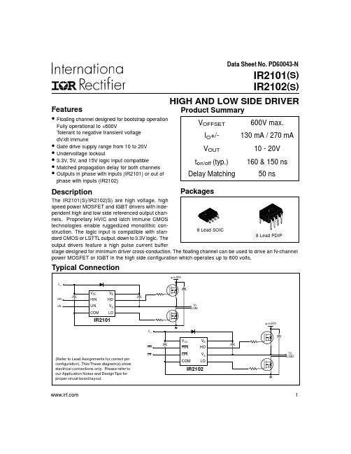
Data Sheet No. PD60043-NFeaturesHIGH AND LOW SIDE DRIVERProduct Summary 1IR2101/IR2102 (S)Absolute Maximum RatingsAbsolute maximum ratings indicate sustained limits beyond which damage to the device may occur. All voltage param-eters are absolute voltages referenced to COM. The thermal resistance and power dissipation ratings are measured under board mounted and still air conditions.Note 1: Logic operational for V S of -5 to +600V. Logic state held for V S of -5V to -V BS . (Please refer to the Design Tip DT97-3 for more details).Recommended Operating ConditionsThe input/output logic timing diagram is shown in figure 1. For proper operation the device should be used within the recommended conditions. The V S offset rating is tested with all supplies biased at 15V differential.IR2101/IR2102 (S)Static Electrical CharacteristicsV BIAS (V CC , V BS ) = 15V and T A = 25°C unless otherwise specified. The V IN , V TH and I IN parameters are referenced to COM. The V O and I O parameters are referenced to COM and are applicable to the respective output leads: HO or LO.Dynamic Electrical CharacteristicsV BIAS (V CC , V BS ) = 15V, C L = 1000 pF and T A = 25°C unless otherwise specified.IR2101/IR2102 (S)IR2101/IR2102 (S) Lead DefinitionsSymbol DescriptionHIN Logic input for high side gate driver output (HO), in phase (IR2101)HIN Logic input for high side gate driver output (HO), out of phase (IR2102)LIN Logic input for low side gate driver output (LO), in phase (IR2101)LIN Logic input for low side gate driver output (LO), out of phase (IR2102)V B High side floating supplyHO High side gate drive outputV S High side floating supply returnV CC Low side and logic fixed supplyLO Low side gate drive outputCOM Low side returnLead Assignments8 Lead PDIP8 Lead SOICIR2101IR2101S8 Lead PDIP8 Lead SOICIR2102IR2102SIR2101/IR2102 (S)Figure 1. Input/Output Timing DiagramHIN LINHO LOHIN LIN Figure 3. Delay Matching Waveform DefinitionsHIN LIN50%50%IR2101/IR2102 (S)IR2101/IR2102 (S)IR2101/IR2102 (S)IR2101/IR2102 (S)IR2101/IR2102 (S)IR2101/IR2102 (S)Case outlines。
This document is downloaded from DR-NTU, Nanyang TechnologicalUniversity Library, Singapore.Design of Low-Power High-SpeedTruncation-Error-Tolerant Adder and ItsApplication in Digital Signal ProcessingNing Zhu,Wang Ling Goh,Weija Zhang,Kiat Seng Yeo,andZhi Hui KongAbstract—In modern VLSI technology,the occurrence of all kinds of errors has become inevitable.By adopting an emerging concept in VLSI design and test,error tolerance(ET),a novel error-tolerant adder(ETA) is proposed.The ETA is able to ease the strict restriction on accuracy,and at the same time achieve tremendous improvements in both the power consumption and speed performance.When compared to its conventional counterparts,the proposed ETA is able to attain more than65%im-provement in the Power-Delay Product(PDP).One important potential application of the proposed ETA is in digital signal processing systems that can tolerate certain amount of errors.Index Terms—Adders,digital signal processing(DSP),error tolerance, high-speed integrated circuits,low-power design,VLSI.I.I NTRODUCTIONIn conventional digital VLSI design,one usually assumes that a us-able circuit/system should always provide definite and accurate results. But in fact,such perfect operations are seldom needed in our nondigital worldly experiences.The world accepts“analog computation,”which generates“good enough”results rather than totally accurate results[1]. The data processed by many digital systems may already contain er-rors.In many applications,such as a communication system,the analog signal coming from the outside world mustfirst be sampled before being converted to digital data.The digital data are then processed and transmitted in a noisy channel before converting back to an analog signal.During this process,errors may occur anywhere.Furthermore, due to the advances in transistor size scaling,factors such as noise and process variations which are previously insignificant are becoming im-portant in today’s digital IC design[2].Based on the characteristic of digital VLSI design,some novel con-cepts and design techniques have been proposed.The concept of error tolerance(ET)[3]–[10]and the PCMOS technology[11]–[13]are two of them.According to the definition,a circuit is error tolerant if:1)it contains defects that cause internal and may cause external errors and2)the system that incorporates this circuit produces acceptable results[3].The“imperfect”attribute seems to be not appealing.However,the need for the error-tolerant circuit[3]–[10]was foretold in the2003In-ternational Technology Roadmap for Semiconductors(ITRS)[2].To deal with error-tolerant problems,some truncated adders/multi-pliers have been reported[14],[15]but are not able to perform well in either its speed,power,area,or accuracy.The“flagged prefixed adder”[14]performs better than the nonflagged version with a1.3%speed enhancement but at the expense of2%extra silicon area.As for the “low-error area-efficientfixed-width multipliers”[15],it may have an area improvement of46.67%but has average error reaching12.4%. Of course,not all digital systems can engage the error-tolerant con-cept.In digital systems such as control systems,the correctness of the output signal is extremely important,and this denies the use of the error-tolerant circuit.However,for many digital signal processing (DSP)systems that process signals relating to human senses such as Manuscript received May28,2008;revised February12,2009.The authors are with the School of Electrical and Electronic Engineering, Nanyang Technological University,Singapore,639798(e-mail:zhuning@ntu. edu.sg).Digital Object Identifier10.1109/TVLSI.2009.2020591hearing,sight,smell,and touch,e.g.,the image processing and speechprocessing systems,the error-tolerant circuits may be applicable[3],[6],[7].The rest of the paper is organized as follows.Section II proposes theaddition arithmetic as well as the structure of the error-tolerant adder(ETA).In Section III,the detailed design of the ETA is explained.Theexperimental results are shown in Section IV.Section V provides anapplication example of the stly,the conclusion of this work ispresented in Section VI.II.E RROR-T OLERANT A DDERBefore detailing the ETA,the definitions of some commonly usedterminologies shown in this paper are given as follows.•Overall error(OE):OE=j R c0R e j,where R e is the result obtained by the adder,and R c denotes the correct result(all theresults are represented as decimal numbers).•Accuracy(ACC):In the scenario of the error-tolerant design,theaccuracy of an adder is used to indicate how“correct”the outputof an adder is for a particular input.It is defined as:ACC= (10(OE=R c))2100%.Its value ranges from0%to100%.•Minimum acceptable accuracy(MAA):Although some errors are allowed to exist at the output of an ETA,the accuracy of an ac-ceptable output should be“high enough”(higher than a threshold value)to meet the requirement of the whole system.Minimum ac-ceptable accuracy is just that threshold value.The result obtained whose accuracy is higher than the minimum acceptable accuracy is called acceptable result.•Acceptance probability(AP):Acceptance probability is the prob-ability that the accuracy of an adder is higher than the minimumacceptable accuracy.It can be expressed as AP=P(ACC> MAA),with its value ranging from0to1.A.Need for Error-Tolerant AdderIncreasingly huge data sets and the need for instant response re-quire the adder to be large and fast.The traditional ripple-carry adder (RCA)is therefore no longer suitable for large adders because of its low-speed performance.Many different types of fast adders,such as the carry-skip adder(CSK)[16],carry-select adder(CSL)[17],and carry-look-ahead adder(CLA)[18],have been developed.Also,there are many low-power adder design techniques that have been proposed [19].However,there are always trade-offs between speed and power. The error-tolerant design can be a potential solution to this problem. By sacrificing some accuracy,the ETA can attain great improvement in both the power consumption and speed performance.B.Proposed Addition ArithmeticIn a conventional adder circuit,the delay is mainly attributed to the carry propagation chain along the critical path,from the least signif-icant bit(LSB)to the most significant bit(MSB).Meanwhile,a sig-nificant proportion of the power consumption of an adder is due to the glitches that are caused by the carry propagation.Therefore,if the carry propagation can be eliminated or curtailed,a great improvement in speed performance and power consumption can be achieved.In this paper,we propose for thefirst time,an innovative and novel addition arithmetic that can attain great saving in speed and power consumption. This new addition arithmetic can be illustrated via an example shown in Fig.1.Wefirst split the input operands into two parts:an accurate part that includes several higher order bits and the inaccurate part that is made up of the remaining lower order bits.The length of each part need not necessary be equal.The addition process starts from the middle1063-8210/$26.00©2009IEEEFig.1.Proposed additionarithmetic.Fig.2.Relationship between AP and MAA.(joining point of the two parts)toward the two opposite directions si-multaneously.In the example of Fig.1,the two 16-bit input operands,A =“1011001110011010”(45978)and B =“0110100100010011”(26899),are divided equally into 8bits each for the accurate and inac-curate parts.The addition of the higher order bits (accurate part)of the input operands is performed from right to left (LSB to MSB)and normal addition method is applied.This is to preserve its correctness since the higher order bits play a more important role than the lower order bits.The lower order bits of the input operands (inaccurate part)re-quire a special addition mechanism.No carry signal will be generated or taken in at any bit position to eliminate the carry propagation path.To minimize the overall error due to the elimination of the carry chain,a special strategy is adapted,and can be described as follow:1)check every bit position from left to right (MSB to LSB);2)if both input bits are “0”or different,normal one-bit addition is performed and the operation proceeds to next bit position;3)if both input bits are “1,”the checking process stopped and from this bit onward,all sum bits to the right are set to “1.”The addition mechanism described can be easily understood from the example given in Fig.1with a final result of “10001110010011111”(72863).The example given in Fig.1should actually yield “10001110010101101”(72877)if normal arithmetic has been applied.The overall error generated can be com-puted as OE =72877072863=14.The accuracy of the adder with respect to these two input operands is ACC =(10(14=72877))2100%=99:98%.Fig.3.Relationship between AP and size ofadder.Fig.4.Hardware implementation of the proposed ETA.By eliminating the carry propagation path in the inaccurate part and performing the addition in two separate parts simultaneously,the overall delay time is greatly reduced,so is the power consumption.C.Relationships Between Minimum Acceptable Accuracy,Acceptance Probability,Dividing Strategy,and Size of Adder The accuracy of the adder is closely related to the input pattern.As-sume that the input of an adder is random;there exists a probability that we can obtain an acceptable result (i.e.,the acceptance proba-bility).The accuracy attribute of an ETA is determined by the dividing strategy and size of adder.In this subsection,the relationships between the minimum acceptable accuracy,the acceptance probability,the di-viding strategy,and the size of adder are investigated.We first consider the extreme situation where we accept only the perfectly correct result.The minimum acceptable accuracy in this “per-fect”situation is 100%.According to the proposed addition arithmetic,we can obtain correct results only when the two input bits on every po-sition in the inaccurate part are not equal to “1”at the same time.We can therefore derive an equation to calculate the acceptance probability associated with the proposed ETA with different bit sizes and dividing strategies.This equation is given as follows:P (ACC =100%)=4N0N23N +2N 0N4N +2N(1)where N t is the total number of bits in the input operand (also regarded as the size of the adder)and N l is the number of bits in the inaccurate part (which is indicating the dividing strategy).Fig.5.Carry-free addition block.(a)Overall architecture and(b)schematic diagram of a modified XOR gate.In situations where the requirement on accuracy can be somewhat re-laxed are investigated,the result will be different.C program is engaged to simulate a16-bit adder that had adopted the proposed addition mech-anism.By checking the output results,we can derive the relationship between the minimum acceptable accuracy and acceptance probability, as depicted in Fig.2.The four curves represent four different dividing strategies,and each of which has been assigned a name“N0M”where “N”denotes the size of the accurate part and“M”for the size of the inaccurate part.For the input patterns,we randomly select10000in-puts from all possible input patterns(i.e.,0–65535).It can be deduced from Fig.2that the lower the minimum acceptable accuracy set,the higher the acceptance probability for the adder.Fig.2also shows that different dividing strategies lead to different accuracy performance. As modern VLSI technology advances,the size of the adder has to in-crease to cater to the application need.The trend of the accuracy perfor-mance of an ETA is therefore investigated in Fig.3.Thefive curves are associated with different minimum acceptable accuracies,95%,96%, 97%,98%,and99%,respectively.Note that all adders follow the same dividing strategy whereby the inaccurate part is three times larger than that of the accurate part.Since small numbers will be calculated at the inaccurate part of the adder,the proposed ETA is best suited for large input patterns.D.Hardware ImplementationThe block diagram of the hardware implementation of such an ETA that adopts our proposed addition arithmetic is provided in Fig.4.This most straightforward structure consists of two parts:an accurate part and an inaccurate part.The accurate part is constructed using a con-ventional adder such as the RCA,CSK,CSL,or CLA.The carry-in of this adder is connected to ground.The inaccurate part constitutes two blocks:a carry-free addition block and a control block.The control block is used to generate the control signals,to determine the working mode of the carry-free addition block.In Section III,a32-bit adder is used as an example for our illustration of the design methodology and circuit implementation of an ETA.III.D ESIGN OF A32-B IT E RROR-T OLERANT A DDERA.Strategy of Dividing the AdderThefirst step of designing a proposed ETA is to divide the adder into two parts in a specific manner.The dividing strategy is based on a guess-and-verify stratagem,depending on the requirements,such as accuracy,speed,and power.First,we define the delay of the proposed adder as T d= max(T h;T l),where T h is the delay in the accurate part and T l is the delay in the inaccurate part.With the proper dividing strategy, we can make T h approximately equal to T l and hence achieve an optimal time delay.With this partition method defined,we then check whether the ac-curacy performance of the adder meets the requirements preset by de-signer/customer.This can be checked very quickly via some software programs.For example,for a specific application,we require the min-imum acceptable accuracy to be95%and the acceptance probability to be98%.The proposed partition method must therefore have at least 98%of all possible inputs reaching an accuracy of better than95%.If this requirement is not met,then one bit should be shifted from the inac-curate part to the accurate part and have the checking process repeated. Also,due to the simplified circuit structure and the elimination of switching activities in the inaccurate part,putting more bits in this part yields more power saving.Having considered the above,we divided the32-bit adder by putting 12bits in the accurate part and20bits in the inaccurate part.B.Design of the Accurate PartIn our proposed32-bit ETA,the inaccurate part has20bits as op-posed to the12bits used in the accurate part.The overall delay is de-termined by the inaccurate part,and so the accurate part need not be a fast adder.The ripple-carry adder,which is the most power-saving conventional adder,has been chosen for the accurate part of the circuit.C.Design of the Inaccurate PartThe inaccurate part is the most critical section in the proposed ETA as it determines the accuracy,speed performance,and power consump-Fig.6.Control block.(a)Overall architecture and(b)schematic implementations of CSGC.tion of the adder.The inaccurate part consists of two blocks:the carry-free addition block and the control block.The carry-free addition block is made up of20modified XOR gates,and each of which is used to gen-erate a sum bit.The block diagram of the carry-free addition block and the schematic implementation of the modified XOR gate are pre-sented in Fig.5.In the modified XOR gate,three extra transistors,M1, M2,and M3,are added to a conventional XOR gate.CTL is the con-trol signal coming from the control block of Fig.6and is used to set the operational mode of the circuit.When CTL=0,M1and M2are turned on,while M3is turned off,leaving the circuit to operate in the normal XOR mode.When CTL=1,M1and M2are both turned off, while M3is turned on,connecting the output node to VDD,and hence setting the sum output to“1.”The function of the control block is to detect thefirst bit position when both input bits are“1,”and to set the control signal on this po-sition as well as those on its right to high.It is made up of20con-trol signal generating cells(CSGCs)and each cell generates a control signal for the modified XOR gate at the corresponding bit position in the carry-free addition block.Instead of a long chain of20cascaded GSGCs,the control block is arranged intofive equal-sized groups,with additional connections between every two neighboring groups.Two types of CSGC,labeled as type I and II in Fig.6(a),are designed,and the schematic implementations of these two types of CSGC are pro-vided in Fig.6(b).The control signal generated by the leftmost cell of each group is connected to the input of the leftmost cell in next group.The extra connections allow the propagated high control signal to“jump”from one group to another instead of passing through all the20cells.Hence,the worst case propagation path[shaded in gray in Fig.6(a)]consists of only ten cells.IV.E XPERIMENTAL R ESULTSTo demonstrate the advantages of the proposed ETA,we simulated the ETA along with four types of conventional adders,i.e.,the RCA, CSK,CSL,and CLA,using HSPICE.All the circuits were imple-mented using Chartered Semiconductor Manufacturing Ltd’s0.18- m CMOS process.The input frequency was set to100MHz,and the sim-ulation results are all tabulated in Table I.HSPICE software was used to construct the models of our proposed ETA and the conventional adders.100sets of inputs were randomly cre-ated using the C program“random()”function.For each set of input,weTABLE IS IMULATION R ESULT FOR ETA V ERSUS C ONVENTIONAL ADDERSran the simulation for each adder and recorded the power consumption. With100sets of results,average power consumption was determined. The worst case input was calculated and used to simulate the delay. The transistor count was derived directly from the HSPICE software. Comparing the simulation results of our proposed ETA with those of the conventional adders(see Table I),it is evident that the ETA per-formed the best in terms of power consumption,delay,and Power-Delay Product(PDP).The PDP of the ETA is noted to be66.29%, 77.44%,83.70%,and75.21%better than the RCA,CSK,CSL,and CLA,respectively.As for transistor count,the proposed ETA is almost as good as the RCA.V.A PPLICATION OF E RROR-T OLERANT A DDERIN D IGITAL S IGNAL P ROCESSINGIn image processing and many other DSP applications,fast Fourier transformation(FFT)is a very important function.The computational process of FFT involves a large number of additions and multiplica-tions.It is therefore a good platform for embedding our proposed ETA. To prove the feasibility of the ETA,we replaced all the common addi-tions involved in a normal FFT algorithm with our proposed addition arithmetic.As we all know,a digital image is represented by a matrix in a DSP system,and each element of the matrix represents the color of one pixel of the image.To compare the quality of images processed by both the conventional FFT and the inaccurate FFT that had incorporated our proposed ETA,we devised the following experiment.An image was first translated to a matrix form and sent through a standard system that made used of normal FFT and normal reverse FFT.The matrix output of this system was then transformed back to an image and presented in Fig.7(a).The matrix of the same image was also processed in a systemFig.7.Images after FFT and inverse FFT.(a)Image processed with conven-tional adder and(b)image processed with the proposed ETA.that used the inaccurate FFT and inaccurate reverse FFT,where both FFTs had incorporated the32-bit ETA described in Section III,with the processed image given in Fig.7(b).Although the two resultant matrices of the same image were dif-ferent,the two pictures obtained(see Fig.7)look almost the same. Fig.7(b)is slightly darker and contains horizontal bands of different shades of gray.With a MAA setting of95%,the AP of the matrix repre-sentation of Fig.7(b)is98.3%as compared to the matrix representation of Fig.7(a).The comparison between the two images in Fig.7shows that the quality loss to the image using our proposed ETA is negligible and can be completely tolerated by human eyes.These simulation results have proven the practicability of the ETA proposed in this paper.VI.C ONCLUSIONIn this paper,the concept of error tolerance is introduced in VLSI de-sign.A novel type of adder,the error-tolerant adder,which trades cer-tain amount of accuracy for significant power saving and performance improvement,is proposed.Extensive comparisons with conventional digital adders showed that the proposed ETA outperformed the conven-tional adders in both power consumption and speed performance.The potential applications of the ETA fall mainly in areas where there is no strict requirement on accuracy or where superlow power consumption and high-speed performance are more important than accuracy.One example of such applications is in the DSP application for portable de-vices such as cell phones and laptops.A CKNOWLEDGMENTW.Zhang would like to thank the Nanyang Technological University (NTU)of Singapore for providing the graduate research scholarship and support.The authors appreciate also the help rendered by Mr.L. Y.Loy.R EFERENCES[1]A.B.Melvin,“Let’s think analog,”in Proc.IEEE Comput.Soc.Annu.Symp.VLSI,2005,pp.2–5.[2]International Technology Roadmap for Semiconductors[Online].Available:/[3]A.B.Melvin and Z.Haiyang,“Error-tolerance and multi-media,”in Proc.2006Int.Conf.Intell.Inf.Hiding and Multimedia SignalProcess.,2006,pp.521–524.[4]M.A.Breuer,S.K.Gupta,and T.M.Mak,“Design and error-toler-ance in the presence of massive numbers of defects,”IEEE Des.TestComput.,vol.24,no.3,pp.216–227,May-Jun.2004.[5]M.A.Breuer,“Intelligible test techniques to support error-tolerance,”in n Test Symp.,Nov.2004,pp.386–393.[6]K.J.Lee,T.Y.Hsieh,and M.A.Breuer,“A novel testing methodologybased on error-rate to support error-tolerance,”in Proc.Int.Test Conf.,2005,pp.1136–1144.[7]I.S.Chong and A.Ortega,“Hardware testing for error tolerant mul-timedia compression based on linear transforms,”in Proc.Defect andFault Tolerance in VLSI Syst.Symp.,2005,pp.523–531.[8]H.Chung and A.Ortega,“Analysis and testing for error tolerant motionestimation,”in Proc.Defect and Fault Tolerance in VLSI Syst.Symp.,2005,pp.514–522.[9]H.H.Kuok,“Audio recording apparatus using an imperfect memorycircuit,”U.S.Patent5414758,May9,1995.[10]T.Y.Hsieh,K.J.Lee,and M.A.Breuer,“Reduction of detected ac-ceptable faults for yield improvement via error-tolerance,”in Proc.Des.,Automation and Test Eur.Conf.Exhib.,2007,pp.1–6.[11]K.V.Palem,“Energy aware computing through probabilisticswitching:A study of limits,”IEEE put.,vol.54,no.9,pp.1123–1137,Sep.2005.[12]S.Cheemalavagu,P.Korkmaz,and K.V.Palem,“Ultra low energycomputing via probabilistic algorithms and devices:CMOS deviceprimitives and the energy-probability relationship,”in Proc.2004Int.Conf.Solid State Devices and Materials,Tokyo,Japan,Sep.2004,pp.402–403.[13]P.Korkmaz,B.E.S.Akgul,K.V.Palem,and L.N.Chakrapani,“Advo-cating noise as an agent for ultra-low energy computing:Probabilisticcomplementary metal-oxide-semiconductor devices and their charac-teristics,”Jpn.J.Appl.Phys.,vol.45,no.4B,pp.3307–3316,2006.[14]J.E.Stine,C.R.Babb,and V.B.Dave,“Constant addition utilizingflagged prefix structures,”in Proc.IEEE Int.Symp.Circuits and Sys-tems(ISCAS),2005.[15]L.-D.Van and C.-C.Yang,“Generalized low-error area-efficientfixed-width multipliers,”IEEE Trans.Circuits Syst.I,Reg.Papers,vol.25,no.8,pp.1608–1619,Aug.2005.[16]M.Lehman and N.Burla,“Skip techniques for high-speed carry prop-agation in binary arithmetic units,”IRE put.,vol.EC-10,pp.691–698,Dec.1962.[17]O.Bedrij,“Carry select adder,”IRE put.,vol.EC-11,pp.340–346,1962.[18]O.MacSorley,“High speed arithmetic in binary computers,”IRE Proc.,vol.49,pp.67–91,1961.[19]Y.Kiat-Seng and R.Kaushik,Low-Voltage,Low-Power VLSI Subsys-tems.New York:McGraw-Hill,2005.。
Block Diagram – PGA Type Package(P1,P7) & CQFP(F2)512Kx8512Kx8512Kx8512Kx8CE 4OEA 0 – A 18I/O 0-7I/O 8-15I/O 16-23I/O 24-318888CE 3WE 4WE 3WE 2WE 1CE 1CE 2Pin Description I/O 0-31Data I/OA 0–18Address Inputs WE 1–4Write Enables CE 1–4Chip Enables OE Output Enable V cc Power Supply GND Ground NCNot ConnectedGeneral DescriptionThe ACT–S512K32V is a High Speed 4 megabit CMOS SRAM Multichip Module (MCM)designed for full temperature range, 3.3V Power Supply,military, space, or high reliability mass memory and fast cache applications.The MCM can be organized as a 512K x 32 bits, 1M x 16bits or 2M x 8 bits device and is input and output TTL compatible. Writing is executed when the write enable (WE)and chip enable (CE) inputs are low. Reading is accomplished when WE is high and CE and output enable (OE) are both low. Access time grades of 17ns, 20ns, 25ns, 35ns and 45ns maximum are standard.The products are designed for operation over the temperature range of -55°C to +125°C and screened under the full military environment. DESC Standard Military Drawing (SMD) part numbers are pending. The ACT -S512K32V is manufactured in Aeroflex’s 80,000ft 2 MIL-PRF-38534certified facility in Plainview,N.Y .Featuress 4 Low Power CMOS 512K x 8 SRAMs in one MCM s Overall configuration as 512K x 32s Input and Output TTL Compatibles 17, 20, 25, 35 & 45ns Access Times, 15ns Available bySpecial Orders Full Military (-55°C to +125°C) Temperature Range s +3.3V Power Supplys Choice of Surface Mount or PGA Type Co-fired Packages:q 68–Lead, Dual-Cavity CQFP (F2), .88"SQ x .20"max (.18"maxthickness available, contact factory for details) (Drops into the 68 Lead JEDEC .99"SQ CQFJ footprint)q 66–Pin, PGA-Type (P1), 1.38"SQ x .245"max q 66–Pin, PGA-Type (P7), 1.08"SQ x .185"maxs Internal Decoupling Capacitors s DESC SMD# PendingCIRCUIT TECHNOLOGY/act1.htmACT -S512K32V High Speed 3.3Volt 16 Megabit SRAM Multichip ModuleAbsolute Maximum RatingsSymbol Rating Range UnitsT C Case Operating T emperatureSpeed 15ns-40 to +85°C Speed 17ns to 45ns-55 to +125°CT STG Storage T emperature-65 to +150°C P D Maximum Package Power DissipationP1,P7 Package F2 Package 3.0W 2.7WØJ-C Hottest Die, Max Thermal Resistance - Junction to CaseP1,P7 Package F2 Package 2.0°C/W 8.0°C/WV G Maximum Signal Voltage to Ground-0.5 to +4.6V T L Maximum Lead Temperature (10 seconds)300°CNormal Operating ConditionsSymbol Parameter Minimum Maximum Units V CC Power Supply Voltage+3.0+3.6V V IH Input High Voltage+2.0V CC + 0.3V V IL Input Low Voltage-0.3+0.8VCapacitance(f = 1MHz, T C = 25°C)Symbol Parameter Maximum UnitsC AD A0 – A18 Capacitance 50pFC OE OE Capacitance50pF C WE Write Enable Capacitance20pFC CE Chip Enable Capacitance20pFC I/O I/O0 – I/O31 Capacitance20pF Capacitance is guaranteed by design but not tested.DC Characteristics(3.0Vdc< V CC < 3.6Vdc, V SS = 0V, T C = -55°C to +125°C, Unless otherwise specified)Parameter Sym Conditions ALL SpeedsMin MaxUnitsInput Leakage Current I LI V CC = Max, V IN=0or V CC10µA Output Leakage Current I LO CE = V IH, OE = V IH, V OUT=0or V CC10µAOperating Supply Current 32 Bit Mode I CC1x32CE = V IL, OE = V IH, f = 5 MHz, V CC = Max,CMOS Compatible600mAStandby Current I SB1CE = V IH, OE = V IH, f = 5 MHz, V CC = Max,CMOS Compatible80mAOperating Supply Current 32 Bit Mode I CC2x32CE = V IL, OE = V IH, f = 50 MHz, V CC =Max, CMOS Compatible750mAStandby Current I SB2CE = V CC, OE = V IH, f = 50 MHz, V CC =Max, CMOS Compatible240mA Output Low Voltage V OL I OL = 8 mA, V CC = Min0.4V Output High Voltage V OH I OH = -4.0 mA, V CC = Min 2.4VAC Characteristics(V CC = 3.3V, V SS = 0V, Tc = -55°C to +125°C) Read CycleParameter Sym–017Min Max–020Min Max–025Min Max–035Min Max–045Min MaxUnitsRead Cycle Time t RC1720253545ns Address Access Time t AA1720253545ns Chip Enable Access Time t ACS1720253545ns Output Hold from Address Change t OH00000ns Output Enable to Output Valid t OE910122535ns Chip Enable to Output in Low Z * t CLZ33333ns Output Enable to Output in Low Z * t OLZ00000ns Chip Deselect to Output in High Z * t CHZ88101515ns Output Disable to Output in High Z * t OHZ88101515ns * Parameters guaranteed by design but not testedWrite CycleParameter Sym–017Min Max–020Min Max–025Min Max–035Min Max–045Min MaxUnitsWrite Cycle Time t WC1720253545ns Chip Enable to End of Write t CW1515203035ns Address Valid to End of Write t AW1515203035ns Data Valid to End of Write t DW1212152030ns Write Pulse Width t WP1313152535ns Address Setup Time t AS00000ns Output Active from End of Write *t OW00000ns Write to Output in High Z * t WHZ811131515ns Data Hold from Write Time t DH00000ns Address Hold Time t AH01222ns * Parameters guaranteed by design but not testedTruth TableMode CE OE WE Data I/O PowerStandby H X X High Z Standby (deselect/power down)Read L L H Data Out ActiveRead L H H High Z Active (deselected)Write L X L Data In ActivePin Numbers & Functions 66 Pins — PGA-TypePin #Function Pin #Function Pin #Function Pin #Function 1I/O 818A 1235I/O 2552WE 32I/O 919Vcc 36I/O 2653CS 33I/O 1020CS 137A 654GND 4A 1321NC 38A 755I/O 195A 1422I/O 339NC 56I/O 316A 1523I/O 1540A 857I/O 307A 1624I/O 1441A 958I/O 298A 1725I/O 1342I/O 1659I/O 289I/O 026I/O 1243I/O 1760A 010I/O 127OE 44I/O 1861A 111I/O 228A 1845V CC 62A 212WE 229WE 146CS 463I/O 2313CS 230I/O 747WE 464I/O 2214GND 31I/O 648I/O 2765I/O 2115I/O 1132I/O 549A 366I/O 2016A 1033I/O 450A 417A 1134I/O 2451A 51.400 SQ 1.000.600 1.000.100.020.016.100 TYP.145MIN.025.035.245MAX Pin 56Pin 66Pin 11Pin 1Bottom ViewMAX TYP TYPTYP.050 DIA TYPTYP"P1" — 1.40" SQ PGA Type PackageSide ViewPin Numbers & Functions 66 Pins — PGA-TypePin #Function Pin #Function Pin #Function Pin #Function 1I/O 818A 1235I/O 2552WE 32I/O 919Vcc 36I/O 2653CE 33I/O 1020CE 137A 654GND 4A 1321NC 38A 755I/O 195A 1422I/O 339NC 56I/O 316A 1523I/O 1540A 857I/O 307A 1624I/O 1441A 958I/O 298A 1725I/O 1342I/O 1659I/O 289I/O 026I/O 1243I/O 1760A 010I/O 127OE 44I/O 1861A 111I/O 228A 1845V CC 62A 212WE 229WE 146CE 463I/O 2313CE 230I/O 747WE 464I/O 2214GND 31I/O 648I/O 2765I/O 2115I/O 1132I/O 549A 366I/O 2016A 1033I/O 450A 417A 1134I/O 2451A 5All dimensions in inches.145MIN1.085 SQ 1.000.600TYP1.000.100 TYPPin 56Pin 66Pin 11Pin 1Bottom ViewMAX .020.016.100.025.185MAX Side View .050 DIA .035TYPTYP TYPTYP "P7" — 1.08" SQ PGA Type PackageOrdering InformationModel NumberDESC Part NumberSpeedPackageACT–S512K32V–017F2Q (Pending)17ns .88"sq CQFP ACT–S512K32V–020F2Q (Pending)20ns .88"sq CQFP ACT–S512K32V–025F2Q (Pending)25ns .88"sq CQFP ACT–S512K32V–035F2Q (Pending)35ns .88"sq CQFP ACT–S512K32V–045F2Q (Pending)45ns .88"sq CQFP ACT–S512K32V–017P1Q (Pending)17ns 1.38"sq PGA-Type ACT–S512K32V–020P1Q (Pending)20ns 1.38"sq PGA-Type ACT–S512K32V–025P1Q (Pending)25ns 1.38"sq PGA-Type ACT–S512K32V–035P1Q (Pending)35ns 1.38"sq PGA-Type ACT–S512K32V–045P1Q (Pending)45ns 1.38"sq PGA-Type ACT–S512K32V–017P7Q (Pending)17ns 1.08"sq PGA-Type ACT–S512K32V–020P7Q (Pending)20ns 1.08"sq PGA-Type ACT–S512K32V–025P7Q (Pending)25ns 1.08"sq PGA-Type ACT–S512K32V–035P7Q (Pending)35ns 1.08"sq PGA-Type ACT–S512K32V–045P7Q(Pending)45ns1.08"sq PGA-Type* Screened to the individual test methods of MIL-STD-883Part Number BreakdownPackage Types & Sizes Surface Mount PackagesF2 = 0.88"SQ 68 Leads Dual-Cavity CQFPThru-Hole PackagesP1 = 1.400"SQ PGA 66 Pins P7 = 1.085"SQ PGA 66 PinsScreeningC = Commercial Temp, 0°C to +70°C I = Industrial T emp, -40°C to +85°C T = Military Temp, -55°C to +125°CM = Military T emp, -55°C to +125°C Screened *Q = MIL-PRF-38534 Compliant/SMDACT–S 512K 32V–020F2MC I R C U I T T E C H N O L O G YAeroflex Circuit Technology Memory Type S = SRAMMemory Depth, Locations Memory Width, Bits Memory Speed, nsOptionsV = +3.3 V Power Supply Aeroflex Circuit Technology 35 South Service RoadPlainview New York 11803 Telephone: (516) 694-6700FAX: (516) 694-6715Toll Free Inquiries: (800) 843-1553Specifications subject to change without notice/act1.htmE-Mail: sales-act@。
Thermometer-to-Binary Decoders for FlashAnalog-to-Digital ConvertersAbstract:Decoders for low power, high-speed flash ADCs are investigated. The sensitivity to bubble errors of the ROM decoder with error correction, ones-counter, 4-level folded Wallace-tree, and multiplexer-based decoder are simulated. The ones-counter and multiplexer-based decoder,corresponding to the error insensitive and hardware efficient cases, are implemented in a 130 nm CMOS SOI technology. Measurements yield an ENOB of about 4.1 bit for both, and energy consumption of 80 pJ and 60 pJ, for the respective decoders. Hence we conclude that the MUX-based decoder seems to be a good choice with respect to area, efficiency, and speed.Key words: Thermometer-to-Binary flash ADCs ConvertersI. INTRODUCTIONApplications like ultra-wideband radio and the read channel in hard disk drives generally require high-speed analog-to-digital conversion with resolution four to six bits. These requirements are commonly satisfied by the flash analog-to-digital converter (ADC) architecture [1] that converts the analog input to a binary outputN parallel comparators, where N is the number of bits in with a single stage of 12the output, followed by a digital decoder. The comparators compare the input with the quantization levels from a set of reference voltages generated by a resistive ladder and produce a logical output depending on the outcome of the comparison. The output pattern from this stage corresponds to thermometer code and is subsequently translated to binary code by the digital decoder, i.e. the thermometer-to-binary decoder. For a low speed converter the input to the decoder is indeed a perfect thermometer code, but for high speed there may be some erroneous bits in the thermometer code, so called bubbles [2]. The bubbles are due to a number of sources [3], e.g., metastability, offset, crosstalk, and bandwidth limitations of the comparators, uncertainty in the effective sampling instant, etc. Hence the decoder must be able to perform well even in the presence of the bubble errors in a high-speed converter.Including requirements on power consumption and throughput, we see that the decoder must be paid significant consideration and trade-off in the design of a high-speed converter. In this work we focus on the design of decoders for low-power, high-speed six-bit ADCs. The work is a part of a larger project where the overall aim is to develop design techniques for implementation of high-performance analog circuits in CMOS silicon-on-insulator technology. We have investigated four types of thermometer-to-binarydecoders presented in Sec. II, through behavioral level simulations of the sensitivity to bubble errors presented in Sec. III, from which we have chosen two decoders that have been implemented in a 130 nm CMOS SOI technology. The measurement results are presented in Sec. IV and the conclusions are given in Sec. V.II. DECODERSFour different types of thermometer-to-binary decoders are presented. Two of them, the ROM and folded Wallace tree decoder,are only studied on behavioral level. The ones-counter decoder and the MUX-based decoder have also been implemented in two flash ADCs in a CMOS silicon-on-insulator technology. The corresponding results are thereby based on transistor level simulation results and measurements.A. ROMA common and straightforward approach to encode the thermometer code is to use a gray or binary-encoded ROM. The appropriate row m in the gray encoded ROM is selected by using a row decoder that has the output of comparator m and the inverse of comparator m + 1 as inputs. The output m of the row decoder, connected to memory row m, is high if the output of comparator m is high and the output of comparator m + 1 is low. The row decoder can be realized by, e.g., a number of 2-input NAND gates, where one input to each NAND gate is inverted. This type of row decoder selects multiple rows if a bubble error occurs, which introduces large errors in the output of the decoder [3], [4]. Considering single bubble errors only, these errors can be corrected by using 3-input NAND gates, as shown in Fig. 1. The 3-input NAND gates remove all bubble errors if they are separated by at least three bits in the thermometer scale. The main advantage of the ROM decoder approach isits regular structure that is straightforward to design. A disadvantage is that more bubble errors are introduced as the conversion speed increases and a more advanced bubble error correction scheme is required. As the complexity of the bubble error correction circuit increases, its propagation delay does in general also increase. The longer propagation delay reduces the maximum sampling rate of the overall decoder if not pipelining is applied. The increased complexity of the circuit consumes more chip area and will likely consume more power [5], [6].Figure 1Another bubble error suppression technique is the butterfly sorting technique presented in [7]. Applying this technique the bubbles are propagated upwards in the thermometer scale until the thermometer code is free from bubbles. Then the ROM decoder is used to encode the bubble-free thermometer code to binary code. In [7] the butterfly sorter only has eight levels. Bubbles further away from the transition level than eight positions cannot be removed. To guarantee that no bubbles will be present in the thermometer output code the depth of the butterfly sorter must be equal to the number of comparators, i.e.,12 N .B. Ones-CounterThe output of a thermometer-to-binary decoder is the number of ones on the input represented in, e.g., gray or binary code. Hence a circuit counting the number of ones in the thermometer code, i.e., a ones-counter, can be used as the decoder [8].The use of a ones-counter gives global bubble error suppression [3], [6], [8]. Another benefit of the approach is that a suitable ones-counter topology may be selected by trading speed for power. From this tradeoff the Wallace tree topology [9], illustrated in Fig. 2, is a good candidate as a decoder for high-speed converters [3], [6], [10].Figure 2In this work we use a tree of full adders (FAs) that reduce the 63 inputs to 10 outputs, as illustrated by Fig. 3. The different signal paths through the decoder are matched, i.e., each signal passes through the same number of full adders, where each input has approximately the same propagation delay to the output. The propagation delay of the signals through the decoder should thereby be approximately the same for all signals. The decoding of the 10 outputs to the binary value is done using MATLAB. The depth of the tree is thereby limited to six levels in the hardware implementation presented in the next section, which enables the ADC to operate at higher speed. In an improved design the complete decoding to a binary output can be accomplishedonchip by introducing pipelining in the decoder. Further optimization of the sizing of each FA can also improve the performance to some degree.C. Folded Wallace TreeFigure 3In a folded flash ADC, the idea is to reduce the amount of hardware by using the same comparator for different reference voltages [11]. This is the idea of the folded Wallace tree decoder shown in Fig. 4 [6]. The size of the Wallace tree and the delay depend on the number of bits that are added, i.e. the width of the base of the tree. The idea is to split the output of the comparators into different intervals. They are multiplexed to a reduced Wallace tree decoder, which is smaller compared with the full one [3]. A full adder may be realized from three 2:1 multiplexers with two multiplexers in the critical path.D. MUX-BasedThe multiplexer-based decoder consists entirely of multiplexers, as illustrated in Fig. 5, where N = 4 bit. It requires less hardware and has a shorter critical path than a ones-counter decoder [3], [5]. In addition it gives bubble error suppression, although the suppression is slightly lower than for a ones-counter decoder [5]. Another advantage of the multiplexer-based decoder is the more regular structure than, e.g., the ones-counter decoder. This is a major benefit in the layout of the circuit. Themultiplexers used in this work are based on transmission gates. An inverter is used as a buffer in each transmission gate multiplexer.Figure 4III. B EHA VIORAL LEVEL SIMULATIONThe effect of the chosen decoder topology on the ADC performance was evaluated by behavioral level simulations for the four different architectures. The timing difference ∆t between the clock signal and the input signal to each compar ator was modeled by a Gaussian distribution, according to ),0(~t N t σ∆。
I II I/O/QI/O/QI/O/Q I/O/Q I/O/Q I/CLKI I I I II I I GNDVcc I/O/QI/O/Q I/O/Q I/O/Q I/O/Q I/O/Q I/O/Q I/O/QI/OEPLCCDIPI/CLKII/O/QII/O/QII/O/QII/O/QII/O/QII/O/QII/O/QII/O/QI/OECopyright © 2004 Lattice Semiconductor Corp. All brand or product names are trademarks or registered trademarks of their respective holders. The specifications and information herein are subject to change without notice.LATTICE SEMICONDUCTOR CORP ., 5555 Northeast Moore Ct., Hillsboro, Oregon 97124, U.S.A.August 2004Tel. (503) 268-8000; 1-800-LATTICE; FAX (503) 268-8556; •HIGH PERFORMANCE E 2CMOS ® TECHNOLOGY —3.5 ns Maximum Propagation Delay —Fmax = 250 MHz—3.0 ns Maximum from Clock Input to Data Output —UltraMOS ® Advanced CMOS Technology•50% to 75% REDUCTION IN POWER FROM BIPOLAR —75mA Typ Icc on Low Power Device —45mA Typ Icc on Quarter Power Device •ACTIVE PULL-UPS ON ALL PINS•E 2CELL TECHNOLOGY —Reconfigurable Logic —Reprogrammable Cells —100% Tested/100% Yields—High Speed Electrical Erasure (<100ms)—20 Year Data Retention•EIGHT OUTPUT LOGIC MACROCELLS—Maximum Flexibility for Complex Logic Designs —Programmable Output Polarity—Also Emulates 20-pin PAL ® Devices with Full Function/Fuse Map/Parametric Compatibility •PRELOAD AND POWER-ON RESET OF ALL REGISTERS —100% Functional Testability •APPLICATIONS INCLUDE:—DMA Control—State Machine Control—High Speed Graphics Processing —Standard Logic Speed Upgrade•ELECTRONIC SIGNATURE FOR IDENTIFICATION •LEAD-FREE PACKAGE OPTIONSDescriptionThe GAL16V8, at 3.5 ns maximum propagation delay time, com-bines a high performance CMOS process with Electrically Eras-able (E 2) floating gate technology to provide the highest speed performance available in the PLD market. High speed erase times (<100ms) allow the devices to be reprogrammed quickly and ef-ficiently.The generic architecture provides maximum design flexibility by allowing the Output Logic Macrocell (OLMC) to be configured by the user. An important subset of the many architecture configura-tions possible with the GAL16V8 are the PAL architectures listed in the table of the macrocell description section. GAL16V8 devices are capable of emulating any of these PAL architectures with full function/fuse map/parametric compatibility.Unique test circuitry and reprogrammable cells allow complete AC,DC, and functional testing during manufacture. As a result, Lattice Semiconductor delivers 100% field programmability and function-ality of all GAL products. In addition, 100 erase/write cycles and data retention in excess of 20 years are specified.Pin ConfigurationI/CLKI I I I I I I I GNDVcc I/O/QI/O/Q I/O/Q I/O/Q I/O/Q I/O/Q I/O/Q I/O/QI/OE)s n (d p T )s n (u s T )s n (o c T )A m (c c I #g n i r e d r O eg a k c a P 5.35.20.3511J L 3-D 8V 61L A G C C L P d a e L -025345118V 61L A G 5-D J L C C L P d a e L -025.7751518V 61L A G 7-D LP P I D c i t s a l P n i P -021518V 61L A G 7-D J L C C L P d a e L -021518V 61L A G 7-D LS -02n i P C I O S 0101755P Q 01-D 8V 61L A G P I D c i t s a l P n i P -0255J Q 01-D 8V 61L A G C C L P d a e L -025118V 61L A G 01-D P L P I D c i t s a l P n i P -025118V 61L A G 01-D J L C C L P d a e L -025118V 61L A G 01-D LS n i P -02C I O S 51210155P Q 51-D 8V 61L A G P I D c i t s a l P n i P -0255J Q 51-D 8V 61L A G C C L P d a e L -0209P L 51-D 8V 61L A G P I D c i t s a l P n i P -0209L 51-D 8V 61L A G J d a e L -02C C L P 09L 51-D 8V 61L A G S C I O S n i P -025*******P Q 52-D 8V 61L A G P I D c i t s a l P n i P -0255J Q 52-D 8V 61L A G C C L P d a e L -0209P L 52-D 8V 61L A G P I D c i t s a l P n i P -0209L 52-D 8V 61L A G J C C L P d a e L -0209L 52-D 8V 61L A G S-02n i P CI O S )s n (d p T )s n (u s T )s n (o c T )A m (c c I #g n i r e d r O eg a k c a P 5.7750318V 61L A G 7-D I P L P I D c i t s a l P n i P -020318V 61L A G 7-D I J L C C L P d a e L -020********V 61L A G 01-D I P L P I D c i t s a l P n i P -020318V 61L A G 01-D I J L C C L P d a e L -025********I P L 51-D 8V 61L A G P I D c i t s a l P n i P -02031I J L 51-D 8V 61L A G C C L P d a e L -020*******I P Q 02-D 8V 61L A G P I D c i t s a l P n i P -0256I J Q 02-D 8V 61L A G C C L P d a e L -025*******I P Q 52-D 8V 61L A G P I D c i t s a l P n i P -0256I J Q 52-D 8V 61L A G C C L P d a e L -02031I P L 52-D 8V 61L A G P I D c i t s a l P n i P -02031IJ L 52-D 8V 61L A G CC L P d a e L -02Industrial Grade SpecificationsConventional PackagingCommercial Grade SpecificationsBlank = Commercial I = IndustrialGradePackage PowerL = Low Power Q = Quarter PowerSpeed (ns)XXXXXXXX XXX XX XDevice Name_P = Plastic DIPPN = Lead-free Plastic DIP J = PLCCJN = Lead-free PLCC S = SOICGAL16V8D Lead-Free PackagingCommercial Grade Specifications)s n (d p T )s n (u s T )s n (o c T )A m (c c I #g n i r e d r O eg a k c a P 5.35.20.3511N J L 3-D 8V 61L A G C C L P d a e L -02e e r F -d a e L 5345118V 61L A G 5-D J L N e e r F -d a e L C C L P d a e L -025.7751518V 61L A G 7-D L N P e e r F -d a e L P I D c i t s a l P n i P -021518V 61L A G 7-D J L N e e r F -d a e L C C L P d a e L -020101755N P Q 01-D 8V 61L A G P I D c i t s a l P n i P -02e e r F -d a e L 55N J Q 01-D 8V 61L A G C C L P d a e L -02e e r F -d a e L 5118V 61L A G 01-D P L N e e r F -d a e L P I D c i t s a l P n i P -025118V 61L A G 01-D J L N e e r F -d a e L C C L P d a e L -025*******P Q 51-D 8V 61L A G N e e r F -d a e L P I D c i t s a l P n i P -0255J Q 51-D 8V 61L A G N e e r F -d a e L C C L P d a e L -0209P L 51-D 8V 61L A G N e e r F -d a e L P I D c i t s a l P n i P -0209L 51-D 8V 61L A G N J e e r F -d a e L d a e L -02C C L P 52512155P Q 52-D 8V 61L A G N e e r F -d a e L P I D c i t s a l P n i P -0255J Q 52-D 8V 61L A G N e e r F -d a e L C C L P d a e L -0209P L 52-D 8V 61L A G N e e r F -d a e L P I D c i t s a l P n i P -0209L 52-D 8V 61L A G NJ e e r F -d a e L CC L P d a e L -02The following discussion pertains to configuring the output logicmacrocell. It should be noted that actual implementation is accom-plished by development software/hardware and is completely trans-parent to the user.There are three global OLMC configuration modes possible: simple, complex, and registered. Details of each of these modes are illustrated in the following pages. Two global bits, SYN and AC0, control the mode configuration for all macrocells. The XOR bit of each macrocell controls the polarity of the output in any of the three modes, while the AC1 bit of each of the macrocells controls the input/output configuration. These two global and 16 individ-ual architecture bits define all possible configurations in a GAL16V8 . The information given on these architecture bits is only to give a better understanding of the device. Compiler software will trans-parently set these architecture bits from the pin definitions, so the user should not need to directly manipulate these architecture bits. The following is a list of the PAL architectures that the GAL16V8 can emulate. It also shows the OLMC mode under which the GAL16V8 emulates the PAL architecture.PAL Architectures GAL16V8 Emulated by GAL16V8Global OLMC Mode 16R8Registered16R6Registered16R4Registered16RP8Registered16RP6Registered16RP4Registered16L8Complex16H8Complex16P8Complex10L8Simple12L6Simple14L4Simple16L2Simple10H8Simple12H6Simple14H4Simple16H2Simple10P8Simple12P6Simple14P4Simple16P2SimpleSoftware compilers support the three different global OLMC modes as different device types. These device types are listed in the table below. Most compilers have the ability to automatically select the device type, generally based on the register usage and output enable (OE) usage. Register usage on the device forces the soft-ware to choose the registered mode. All combinatorial outputs with OE controlled by the product term will force the software to choose the complex mode. The software will choose the simple mode only when all outputs are dedicated combinatorial without OE control. The different device types listed in the table can be used to override the automatic device selection by the software. For further details, refer to the compiler software manuals.When using compiler software to configure the device, the user must pay special attention to the following restrictions in each mode. In registered mode pin 1 and pin 11 are permanently configured as clock and output enable, respectively. These pins cannot be con-figured as dedicated inputs in the registered mode.In complex mode pin 1 and pin 11 become dedicated inputs and use the feedback paths of pin 19 and pin 12 respectively. Because of this feedback path usage, pin 19 and pin 12 do not have the feedback option in this mode.In simple mode all feedback paths of the output pins are routed via the adjacent pins. In doing so, the two inner most pins ( pins 15 and 16) will not have the feedback option as these pins are always configured as dedicated combinatorial output.Registered Complex Simple Auto Mode SelectABEL P16V8R P16V8C P16V8AS P16V8 CUPL G16V8MS G16V8MA G16V8AS G16V8LOG/iC GAL16V8_R GAL16V8_C7GAL16V8_C8GAL16V8 OrCAD-PLD"Registered"1"Complex"1"Simple"1GAL16V8A PLDesigner P16V8R2P16V8C2P16V8C2P16V8A TANGO-PLD G16V8R G16V8C G16V8AS3G16V81) Used with Configuration keyword.2) Prior to Version 2.0 support.3) Supported on Version 1.20 or later.V IL Input Low Voltage Vss – 0.5—0.8V V IH Input High Voltage2.0—Vcc+1V I IL 1Input or I/O Low Leakage Current 0V ≤ V IN ≤ V IL (MAX.)——–100µA I IH Input or I/O High Leakage Current3.5V ≤ V IN ≤ V CC——10µA V OL Output Low Voltage I OL = MAX. V in = V IL or V IH ——0.5V V OH Output High Voltage I OH = MAX. V in = V IL or V IH2.4——V I OLLow Level Output CurrentL-3/-5 & -7 (Ind. PLCC)——16mA L-7 (Except Ind. PLCC)/-10/-15/-25——24mAQ-10/-15/-20/-25I OH High Level Output Current ——–3.2mA I OS 2Output Short Circuit CurrentV CC = 5V V OUT = 0.5V T A = 25°C–30—–150mACommercial Devices:Ambient Temperature (T A )...............................0 to 75°C Supply voltage (V CC )with Respect to Ground .....................+4.75 to +5.25V Industrial Devices:Ambient Temperature (T A )...........................–40 to 85°C Supply voltage (V CC )with Respect to Ground .....................+4.50 to +5.50VSupply voltage V CC ......................................–0.5 to +7V Input voltage applied ..........................–2.5 to V CC +1.0V Off-state output voltage applied .........–2.5 to V CC +1.0V Storage Temperature ................................–65 to 150°C Ambient Temperature withPower Applied........................................–55 to 125°C1.Stresses above those listed under the “Absolute Maximum Ratings” may cause permanent damage to the device. These are stress only ratings and functional operation of the device at these or at any other conditions above those indicated in the operational sections of this specification is not implied (while programming, follow the programming specifications).Over Recommended Operating Conditions (Unless Otherwise Specified)SYMBOLPARAMETER CONDITIONMIN.TYP .3MAX.UNITS COMMERCIAL I CC Operating PowerV IL = 0.5V V IH = 3.0V L -3/-5/-7/-10—75115mA Supply Currentf toggle = 15MHz Outputs OpenL-15/-25—7590mA Q-10/-15/-25—4555mAINDUSTRIAL I CC Operating PowerV IL = 0.5V V IH = 3.0V L -7/-10/-15/-25—75130mA Supply Currentf toggle = 15MHz Outputs OpenQ -20/-25—4565mA1) The leakage current is due to the internal pull-up resistor on all pins. See Input Buffer section for more information.2) One output at a time for a maximum duration of one second. Vout = 0.5V was selected to avoid test problems caused by tester ground degradation. Characterized but not 100% tested.3) Typical values are at Vcc = 5V and T A = 25 °Ct pd A Input or I/O to Comb. Output 1 3.51517.5ns t co A Clock to Output Delay 131415ns t cf 2—Clock to Feedback Delay— 2.5—3—3ns t su —Setup Time, Input or Feedback before Clock ↑ 2.5—3—5—ns t h—Hold Time, Input or Feedback after Clock ↑0——0—ns A Maximum Clock Frequency with 182—142.8—100—MHz External Feedback, 1/(tsu + tco)A Maximum Clock Frequency with 200—166—125—MHz Internal Feedback, 1/(tsu + tcf)AMaximum Clock Frequency with 250—166—125—MHz No Feedbackt wh —Clock Pulse Duration, High 2 4—3 4—4—ns t wl —Clock Pulse Duration, Low 2 4—3 4—4—ns t en B Input or I/O to Output Enabled — 4.51619ns B OE to Output Enabled — 4.51616ns t disC Input or I/O to Output Disabled — 4.51519ns COE to Output Disabled—4.51516ns-5 MIN.MAX.SYMBOLPARAMETER MAXIMUM*UNITS TEST CONDITIONS C I Input Capacitance 8pF V CC = 5.0V, V I = 2.0V C I/OI/O Capacitance8pFV CC = 5.0V, V I/O = 2.0V*Characterized but not 100% tested.Over Recommended Operating Conditions-7 MIN.MAX.UNITS PARAMETERTESTCOND 1.DESCRIPTIONCOM / INDCOM1) Refer to Switching Test Conditions section.2) Calculated from f max with internal feedback. Refer to fmax Descriptions section.3) Refer to fmax Descriptions section. Characterized but not 100% tested.4) Characterized but not 100% tested.f max 3-3 t pd A Input or I/O to Comb. Output 310315320325ns t co A Clock to Output Delay 27210211212ns t cf 2—Clock to Feedback Delay—6—8—9—10ns t su —Setup Time, Input or Fdbk before Clk ↑7.5—12—13—15—ns t h—Hold Time, Input or Fdbk after Clk ↑0—0—0—0—ns AMaximum Clock Frequency with 66.7—45.5—41.6—37—MHzExternal Feedback, 1/(tsu + tco)f max 3A Maximum Clock Frequency with 71.4—50—45.4—40—MHz Internal Feedback, 1/(tsu + tcf)AMaximum Clock Frequency with 83.3—62.5—50—41.6—MHz No Feedbackt wh —Clock Pulse Duration, High 6—8—10—12—ns t wl —Clock Pulse Duration, Low 6—8—10—12—ns t en B Input or I/O to Output Enabled 110—15—18—20ns B OE to Output Enabled 110—15—18—20ns t dis C Input or I/O to Output Disabled 110—15—18—20ns COE to Output Disabled110—15—18—20nsOver Recommended Operating ConditionsUNITS -25MIN.MAX.-20 MIN.MAX.-15 MIN.MAX.-10 MIN.MAX.PARAM.DESCRIPTIONTESTCOND 1.COM / INDCOM / INDINDCOM / INDSYMBOLPARAMETER MAXIMUM*UNITS TEST CONDITIONS C I Input Capacitance 8pF V CC = 5.0V, V I = 2.0V C I/OI/O Capacitance8pFV CC = 5.0V, V I/O = 2.0V*Characterized but not 100% tested.1) Refer to Switching Test Conditions section.2) Calculated from f max with internal feedback. Refer to fmax Descriptions section.3) Refer to fmax Descriptions section. Characterized but not 100% tested.Vol vs Iol00.20.40.610203040Iol (mA)V o l (V )Voh vs Ioh1234501020304050Ioh (mA)V o h (V )Voh vs Ioh33.23.43.63.8401234Ioh (mA)V o h (V )Normalized Icc vs Vcc0.80.911.11.24.504.755.00 5.25 5.50Supply Voltage (V)N o r m a l i z e d I c cNormalized Icc vs Temp0.70.80.911.11.21.3-55-25255075100125Temperature (deg. C)N o r m a l i z e d I c cNormalized Icc vs Freq.0.80.911.11.21.31.40255075100Frequency (MHz)N o r m a l i z e d I c cDelta Icc vs Vin (1 input)24680.511.522.533.54Vin (V)D e l t a I c c (m A )Input Clamp (Vik)0102030405060-2-1.5-1-0.5Vik (V)I i k (m A )。
高速低功耗双尾比较器的设计任志德;郭春生【摘要】In order to optimize the speed and power of comparator,a new double tail comparator has been proposed based on an existing one.We increase the speed of the comparator by additional positive feedback path of cross-cou⁃pling. But the number of branches of the power to the ground the number of devices in the circuit are reduced to save power consumption.Simulation results show that the maximum operating frequency can be processed from the original 1.7 GHz to 2.5 GHz. The power consumption can be saved significantly with the increasing operating fre⁃quency.When the operating frequency is at 1.7 GHz,the consumption can save on 41.45%,and power delay product can increase 62.33%. The proposed two-tailed comparator is more suitable for high-speed,low-power analog-to-digi⁃tal conversion circuit.%针对比较器速度和功耗两大指标的优化,对一款新提出的双尾比较器进行了改善和提高。