三端可调恒流源LM334及其应用
- 格式:pdf
- 大小:109.99 KB
- 文档页数:3
基于LM334芯片做的1mA恒流源电路最近因为工作需要,设计了一款基于LM334MX/NOPB的1mA恒流源电路,根据实际效果来看,也基本能够满足设计需求,虽然网上已经有很多关于这个设计的帖子、芯片手册上也有相关说明,但我还是想把自己在调试过程中遇到的问题做一个整理,然后共享出来让更多的人看到,最大限度避免有人跟我走同样的弯路,提高我们这些苦逼硬件工程师的工作效率,如果文中内容有错误的地方也欢迎大家指出来,我们一起进步。
最近手头接到一个项目,需要做一个位移传感器,经项目小组开会讨论,最后决定电路设计以恒流源为基础,采集负载端接入电路不同电阻情况时横流输入端的不同电压,以确定此时传感器的不同行程。
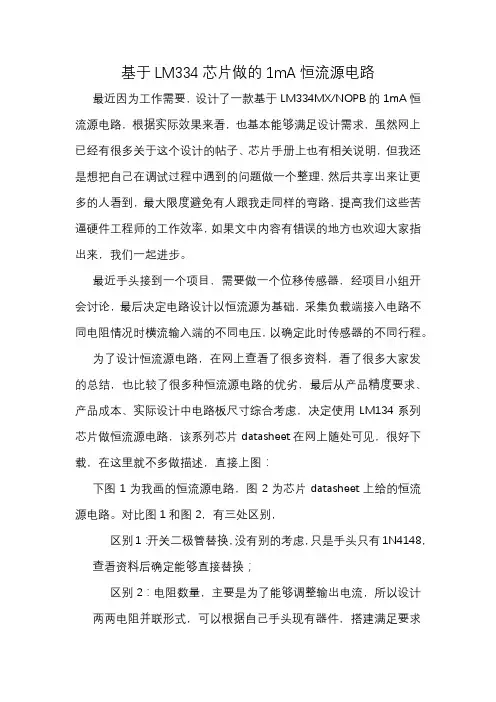
为了设计恒流源电路,在网上查看了很多资料,看了很多大家发的总结,也比较了很多种恒流源电路的优劣,最后从产品精度要求、产品成本、实际设计中电路板尺寸综合考虑,决定使用LM134系列芯片做恒流源电路,该系列芯片datasheet在网上随处可见,很好下载,在这里就不多做描述,直接上图:下图1为我画的恒流源电路,图2为芯片datasheet上给的恒流源电路。
对比图1和图2,有三处区别,区别1:开关二极管替换,没有别的考虑,只是手头只有1N4148,查看资料后确定能够直接替换;区别2:电阻数量,主要是为了能够调整输出电流,所以设计两两电阻并联形式,可以根据自己手头现有器件,搭建满足要求的电阻。
(图1中右侧标注为1mA时的电阻理想值)区别3:恒流源输出端串0Ω电阻,只是为了调试中能够方便使用万用表测量电路是否横流而设计图1 恒流源电路图2 官方恒流源电路注意三点:1、图1中芯片供电为12V,这个电压值可根据自己实际需求调整,芯片本身可兼容0~40V供电电压,而根据后端恒流源电流输入的负载阻抗可计算出芯片输出端最高电压,保证工作电压与输出端电压最少1V以上压差,才能保证芯片输出横流;2、计算公式公式1 温飘计算公式公式2 恒流计算公式设计过程中,可根据电路实际所需的电流值,将两个电阻设为未知数,列出一个二元一次方程组(注意不要使用资料中给出的0.134V数值,该值对于精度要求较高的电路并不太适用),接下来就是最基础的初中知识啦。
设计要求;设计一可调恒流源电路,输出电流范围2mA~20mA,最小刻度0.5mA,波动小于0.1 mA可调恒流源设计摘要本系统以直流电流源为核心,MC34063为主控制器,通过电位器来设置直流电源的输出电流,并可由数码管显示实际输出电流值和电流设定值。
本系统由单片机程控输出数字信号,经过D/A转换器(AD0804)输出模拟量,再经过运算放大器隔离放大,控制输出功率管的基极,随着功率管基极电压的变化而输出不同的电流。
单片机系统还兼顾对恒流源进行实时监控,输出电流经过电流/电压转变后,通过A/D转换芯片,实时把模拟量转化为数据量,再经单片机分析处理,通过数据形式的反馈环节,使电流更加稳定,这样构成稳定的压控电流源。
关键字:MC34063,恒流源,单片机,A/DAdjustable constant current source designAbstractIn this system the DC source is center and MC34063 is main controller, output current of DC power can be set by a potentiometer which step level reaches 1mA, while the real output current and the set value can be displayed by LED. In the system, the digitally programmable signal from SCM is converted to analog value by DAC (AD0804), then the analog value which is isolated and amplified by operational amplifiers, is sent to the base electrode of power transistor, so an adjustable output current can be available with the base electrode voltage of power transistor. On the other hand, The constant current source can be monitored by the system real-timely, its work process is that output current is converted voltage, then its analog value is converted to digital value by ADC, finally the digital value as a feedback loop is processed by so that output current is more stable, so a stable voltage-controlled constant current power is designed..Key wards:MC34063, constant current source, single chip microcomputer, A/D目录1 引言.................................................................................................................................... - 3 -1.1研究目的和意义...................................................................................................... - 3 -1.2国内外发展状况...................................................................................................... - 3 -1.2.1国外发展现状............................................................................................... - 4 -1.2.2国内发展现状............................................................................................... - 4 -1.3 本文欲采取的研究方法......................................................................................... - 5 -2 设计方案............................................................................................................................ - 5 -2.1 总体方案................................................................................................................. - 6 -2.2 MC34063恒流源系统.............................................................................................. - 7 -2.3 电流显示系统......................................................................................................... - 8 -2.3.1 单片机STC10F08XE..................................................................................... - 9 -2.3.2单片机晶振部分.................................................................................................. - 10 -2.3.3 单片机复位部分........................................................................................ - 11 -2.3.4 数码管显示部分........................................................................................ - 12 -2.3.5 电流采样处理部分.................................................................................... - 13 -2.4 整体电路............................................................................................................... - 13 -2.5 系统PCB图.................................................................................................................. - 14 -3 硬件介绍.......................................................................................................................... - 14 -3.1 MC34063恒流源系统............................................................................................ - 14 -3.1.1 MC34063介绍............................................................................................. - 15 -3.2 电流显示系统....................................................................................................... - 16 -3.2.1 单片机STC10F08XE................................................................................... - 17 -3.2.2 模数转换介绍............................................................................................ - 19 -3.2.3 显示部分.................................................................................................... - 21 -4 软件设计.......................................................................................................................... - 21 -4.1 单片机选择........................................................................................................... - 22 -4.2 编程软件介绍....................................................................................................... - 22 -4.3 系统软件流程....................................................................................................... - 22 -4.4 单片机程序........................................................................................................... - 23 -5 实物说明及实验部分...................................................................................................... - 29 -5.1 实物说明............................................................................................................... - 29 -5.2 误差计算............................................................................................................... - 29 -5.3 实验部分............................................................................................................... - 30 -5.3.1 第一组实验................................................................................................ - 30 -5.3.2 第二组实验................................................................................................ - 33 - 总结.................................................................................................................................. - 35 - 参考文献.............................................................................................................................. - 36 - 致谢.................................................................................................................................. - 38 -1 引言恒流源又叫电流源、稳流源,理想的恒流源具有以下特点:不因负载(输出电压)变化而改变;不因环境温度变化而改变;内阻为无限大。
基于FPGA的振动信号采集系统设计及实现王凌伟;樊瑞;秦冲;赵君【摘要】针对机械设备运行中的振动监控,设计振动信号采集系统,提出了一种基于FPGA的振动信号采集系统的设计方案.重点阐述了系统硬件结构组成、信号调理电路和数据采集模块的设计,同时对A/D采样的控制逻辑进行了讨论.经试验验证表明,该系统可达到采样率10 K每秒、采集精度16位,能够满足实时性和精度要求.【期刊名称】《山西电子技术》【年(卷),期】2015(000)003【总页数】4页(P22-24,26)【关键词】加速度传感器;振动信号;信号采集;FPGA【作者】王凌伟;樊瑞;秦冲;赵君【作者单位】中航工业西安航空计算技术研究所,陕西西安710065;中航工业西安航空计算技术研究所,陕西西安710065;中航工业西安航空计算技术研究所,陕西西安710065;中航工业西安航空计算技术研究所,陕西西安710065【正文语种】中文【中图分类】TP212;TP274.2;TN9193随着生产机械、运输机械或工程结构向着高速、高效、高精度和大型化发展,机械设备的任何部件出现故障都可能降低加工精度,带来较大的经济损失,甚至危及人身安全。
机械部件的振动状态监测已成为生产中的一个必不可少的环节,并对相应机械部件进行早期的故障预测[1,2]。
文中采用FPGA 为核心开发振动信号采集系统,对数据采集模块及通讯模块进行了同步设计。
1 总体设计振动信号采集系统以FPGA 芯片为核心,通过A/D 转换芯片采集振动信号,然后通过RS-422 串行总线接口将采集的数据传输给上位机,在故障诊断软件以作出相应的诊断处理。
振动信号采集系统的硬件按照功能模块可以划分为信号调理电路、A/D 转换电路、FPGA 控制逻辑和RS-422 接口转换电路[3],系统硬件结构如图1 所示。
图1 系统硬件结构框图系统硬件各个功能模块的作用如下:1)信号调理电路:信号调理电路主要对由集成电路压电式(Integrated Circuit Piezoelectricity,ICP)加速度传感器采集到的振动信号进行调理驱动、放大和抗混叠滤波处理,使模数转换器(Analog to Digital Converter,ADC)芯片能够获取该振动信号,并作出进一步处理工作。
重庆大学本科学生毕业设计(论文)传感器及电源通用控制器的设计学生:赵磊学号:********指导教师:***专业:机械电子工程重庆大学机械工程学院二O一一年六月Graduation Design(Thesis) of Chongqing University Design of Senor and Source General ControllerUndergraduate: Zhao LeiSupervisor: Prof. Yin AijunMajor: Mechanical-electronic EngineeringCollege of Mechanical EngineeringChongqing UniversityJune 2011摘要测试技术与测试仪器是获取信息、分析和处理测量数据的关键技术和手段,是从事科学研究、产品质量分析检验与控制不可获取的工具。
机械科学里测试也是很重要的一个研究分支,机械里面的测试有机械的振动、噪声等测试,其中机械振动的测试及工程上很重要的一部分,随着生产的发展和科学理论技术的水平的提高,现代的振动测试过采用电测法,但是在机械行业里面机械式的测振法仍然是以振动传感器为理论基础的。
现在工程测试中广泛采用的机械量的电测原理和技术,也就是首先使用各种转换装置——传感器来将不同信号的物理特征转为具有物理特性的电信号。
所以传感器在机械测试中是占有很重要的地位的。
要做好机械测试这一块的工作,我得做好测试整个过程中的每一步。
而传感器要很好的工作它肯定是需要完善的调理电路。
而在机械的测试技术中常用到得就是两种传感器,普通的压电式加速度传感器和ICP加速度传感器,两者的应用都很广泛,在现代的机械测试中都应用的很多。
本文将为读者介绍两种传感器的结构,在测试中的应用,以及两种传感器使用的差别。
两种传感器之间又由于内部有小的细微差别使他们在测试的时候拥有不同的测试通道,这样我们的测试仪器上就需要给两种传感器配备不同的通道口,是仪器显得繁重而且给测试工作带来烦恼,在本文中将以简化测试人员的工作,简化测试仪器的为目的设计一个传感器自动识别及调理电路来实现传感器通道口的共用问题,同时也解决ICP传感器的恒流源供电。
多用途稳压集成电路测试仪的工作原理本测试仪电原理图见下图,主要对以下五大类元器件进行测试:1、电流源元件;2、精密基准电压源;3、可调的正负电压输出集成稳压器;4、固定的正电压输出集成稳压器;5、固定的负电压输出集成稳压器等。
测量品种各类常用元器件测试的等效电路图见下图,其中:下图a为三端可调电流源LM134/234/334的测试原理图。
为简化测试线路,便于公用电阻,将可调电流源的电流测试转换为类似LM317可调集成稳压器基准电压Vref的测试。
在常温下图1中的设定电流约为8.3mA左右,可作为LM317、337测试时的最小负载电流。
此时在R2(150Ω)电阻上的压降约为1.25V左右。
如果数字万用表测得的电压在1.25V左右,且改变稳压电源的输出电压时其读数基本不变,则表明元件是良好的。
下图b、c、d、e为各种精密基准电压源的测试原理图。
其中:LM335的基准电压在2.98V 左右;LM336的基准电压在2.49V左右;LM385的基准电压有1.25V和2.5V两种;TL431的基准电压在2.5V左右,还有TLV431的基准电压在1.25V左右。
下图f为LM317可调正电压输出集成稳压器的测试原理图。
其基准电压Vref在1.25V左右。
测试时的最小负载电流在8.3mA左右。
可满足正常工作时对最小负载电流的要求。
下图g为LM337可调负电压输出集成稳压器的测试原理图。
其基准电压Vref在-1.25V左右,最小负载电流也在8.3mA左右。
下图h是对LM337L的测试原理图,②、③管脚正好与LM337的管脚相反。
下图i为LM78xx固定正电压输出集成稳压器的测试原理图。
其中XX为该器件输出的稳压电压,有5V、6V、8V、9V、12V、15V、18V、24V等多种电压。
下图j为LM78Lxx固定正电压输出稳压器的测试原理图。
③、①管脚正好与LM78xx时的管脚相反。
下图k为LM79xx固定负电压输出集成稳压器的测试原理图。
基于 STM32的晶体管特性曲线测试仪刘士兴;刘宏银;赵博;鲁迎春;易茂祥【摘要】A transistor characteristic curve tester has been designed,which is based on STM32F103.The input ladder current of the base of the triode under test is implemented by adopting digital potentiometer,and the base drive current is 0-1 60 μA whose resolution is 0.1 μA.The regulation of the collector scanning voltage is achieved by the output of the three-terminal voltage regulator circuit which is controlled by embedded DAC, and the output ranges 0-30 V whose highest resolution is 3.18 mV.First of all,a sense resistor has been used to change the determined current into voltage ,which is amplified by instrumentation amplifier and sampled by the embedded ADC,also the median average filtering method has been used to filter the sampling disturbance. The measured parameters are processed by STM32F103 processor to map the input-output characteristic curve and have a real-time display of the amplification h FE on LCD.The tester also has the function of communication with PC which is convenient for further processing.%设计了一种以 STM32F103VET6为核心的晶体管输入输出特性曲线测试仪.通过数字电位器实现对待测三极管基极输入电流的阶梯控制,基极驱动电流0~160μA,分辨率达到0.1μA;通过内嵌 DAC 控制三端稳压电路的输出实现集电极扫描电压的调节,输出范围0~30 V,最高分辨率3.18 mV;电流的测量首先通过采样电阻转换为待测电压,经仪表放大器进行放大后由内嵌 ADC 进行采样,采用中位值平均滤波法滤除采样干扰.由 STM32F103VET6处理器对所测得参数运算处理,绘制晶体管输入输出特性曲线,通过 LCD实时显示晶体管特性曲线及放大倍数 h FE 值;测试仪还具有与上位机通信的功能,方便实现对所测数据做进一步处理.【期刊名称】《实验技术与管理》【年(卷),期】2015(000)011【总页数】5页(P86-90)【关键词】晶体管特性曲线;嵌入式处理器;数字滤波;LCD 显示【作者】刘士兴;刘宏银;赵博;鲁迎春;易茂祥【作者单位】合肥工业大学电子科学与应用物理学院,安徽合肥 230009;合肥工业大学电子科学与应用物理学院,安徽合肥 230009;合肥工业大学电子科学与应用物理学院,安徽合肥 230009;合肥工业大学电子科学与应用物理学院,安徽合肥 230009;合肥工业大学电子科学与应用物理学院,安徽合肥 230009【正文语种】中文【中图分类】TN32晶体管特性曲线图示仪能够测量半导体晶体管的静态参数[1],显示晶体管的输入、输出特性曲线,在高校电子信息类专业的教学中获得了广泛的应用[2]。
赛区编号:18-012011年全国大学生电子设计竞赛简易自动电阻测试仪设计与总结报告组别:高职高专题号:G完成日期:2011年9月3日简易自动电阻测试仪设计与总结报告摘要本设计完成了一种通过检测电压测量电阻的恒流源式简单自动电阻测量仪。
它以单片STC89C52为核心,通过恒流源模块、A/D转换模块和显示模块电阻实现了电阻在大范围内测量,并且能在测量量程为100Ω、1kΩ、10kΩ、10MΩ四档中自由切换,测量精度高,并且具有电阻筛选功能、自动测量和显示电位器阻值随旋转角度变化的曲线。
在恒流源设计部分采用微恒流源和压控电流源,通过4051电子开关的程控实现了各档位的自由切换,此部分性能优越,稳定性较高。
整机系统均达到设计要求的指标。
关键词:恒流源,程控控制,A/D转换1目录摘要 (1)目录 (2)§1.设计任务与要求 (3)1.1 设计任务 (3)1.2 技术指标 (3)1.3 题目评析 (3)§2.系统方案 (3)2.1 各种方案比较与选择 (3)2.2 方案描述 (4)3理论分析与计算 (5)3.1电阻测量原理 (5)3.2自动换量程原理 (5)4 电路设计与程序设计 (6)4.1电路设计 (6)4.1.1微恒流源电路 (6)4.1.2压控电流源电路 (7)4.1.3有源滤波电路 (8)4.1.4 A/D采样电路 (8)4.2程序设计 (9)4.2.1程序总流程图 (9)4.2.2程序主要模块流程图 (10)5测试方案与测试结果 (12)5.1测试方案及测试条件 (12)5.1.1测试方案 (12)5.1.2测试仪器 (12)5.2测试结果 (12)6结论 (13)参考文献 (14)附录 (15)附录1 元器件清单 (15)附录2 总设计思想图 (16)2§1.设计任务与要求1.1 设计任务设计并制作一台简易自动电阻测试仪。
1.2 技术指标基本要求(1)测量量程为100Ω、1kΩ、10kΩ、10MΩ四档。
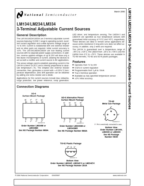
LM134/LM234/LM3343-Terminal Adjustable Current SourcesGeneral DescriptionThe LM134/LM234/LM334are 3-terminal adjustable current sources featuring 10,000:1range in operating current,excel-lent current regulation and a wide dynamic voltage range of 1V to 40V.Current is established with one external resistor and no other parts are required.Initial current accuracy is ±3%.The LM134/LM234/LM334are true floating current sources with no separate power supply connections.In addi-tion,reverse applied voltages of up to 20V will draw only a few dozen microamperes of current,allowing the devices to act as both a rectifier and current source in AC applications.The sense voltage used to establish operating current in the LM134is 64mV at 25˚C and is directly proportional to abso-lute temperature (˚K).The simplest one external resistor connection,then,generates a current with ≈+0.33%/˚C tem-perature dependence.Zero drift operation can be obtained by adding one extra resistor and a diode.Applications for the current sources include bias networks,surge protection,low power reference,ramp generation,LED driver,and temperature sensing.The LM234-3and LM234-6are specified as true temperature sensors with guaranteed initial accuracy of ±3˚C and ±6˚C,respectively.These devices are ideal in remote sense applications be-cause series resistance in long wire runs does not affect ac-curacy.In addition,only 2wires are required.The LM134is guaranteed over a temperature range of −55˚C to +125˚C,the LM234from −25˚C to +100˚C and the LM334from 0˚C to +70˚C.These devices are available in TO-46hermetic,TO-92and SO-8plastic packages.Featuresn Operates from 1V to 40V n 0.02%/V current regulationn Programmable from 1µA to 10mA n True 2-terminal operationn Available as fully specified temperature sensor n±3%initial accuracyConnection DiagramsSO-8Surface Mount PackageDS005697-24Order Number LM334M orLM334MXSee NS Package Number M08ASO-8Alternative Pinout Surface Mount PackageDS005697-25Order Number LM334SM orLM334SMXSee NS Package Number M08ATO-46Metal Can PackageDS005697-12V −Pin is electrically connected to case.Bottom ViewOrder Number LM134H,LM234H or LM334H See NS Package Number H03HTO-92Plastic PackageDS005697-10Bottom ViewOrder Number LM334Z,LM234Z-3or LM234Z-6See NS Package Number Z03AMarch 2000LM134/LM234/LM3343-Terminal Adjustable Current Sources©2000National Semiconductor Corporation Absolute Maximum Ratings (Note 1)If Military/Aerospace specified devices are required,please contact the National Semiconductor Sales Office/Distributors for availability and specifications.V +to V −Forward Voltage LM134/LM234/LM33440V LM234-3/LM234-630V V +to V −Reverse Voltage 20V R Pin to V −Voltage 5V Set Current10mA Power Dissipation400mW ESD Susceptibility (Note 6)2000VOperating Temperature Range (Note 5)LM134−55˚C to +125˚CLM234/LM234-3/LM234-6−25˚C to +100˚C LM3340˚C to +70˚C Soldering InformationTO-92Package (10sec.)260˚C TO-46Package (10sec.)300˚C SO PackageVapor Phase (60sec.)215˚C Infrared (15sec.)220˚C See AN-450“Surface Mounting Methods and Their Effect on Product Reliability”(Appendix D)for other methods of sol-dering surface mount devices.Electrical Characteristics (Note 2)ParameterConditionsLM134/LM234LM334Units MinTypMax MinTypMax Set Current Error,V +=2.5V,10µA ≤I SET ≤1mA 36%(Note 3)1mA <I SET ≤5mA 58%2µA ≤I SET <10µA 812%Ratio of Set Current to 100µA ≤I SET ≤1mA 141823141826Bias Current1mA ≤I SET ≤5mA 14142µA ≤I SET ≤100µA 18231826Minimum Operating Voltage2µA ≤I SET ≤100µA 0.80.8V 100µA <I SET ≤1mA0.90.9V 1mA <I SET ≤5mA1.0 1.0V Average Change in Set Current 2µA ≤I SET ≤1mA with Input Voltage1.5≤V +≤5V 0.020.050.020.1%/V 5V ≤V +≤40V 0.010.030.010.05%/V 1mA <I SET ≤5mA 1.5V ≤V ≤5V 0.030.03%/V 5V ≤V ≤40V0.020.02%/VTemperature Dependence of 25µA ≤I SET ≤1mA0.96TT1.04T0.96TT1.04T Set Current (Note 4)Effective Shunt Capacitance1515pFNote 1:.“Absolute Maximum Ratings”indicate limits beyond which damage to the device may occur.Operating Ratings indicate conditions for which the device is functional,but do not guarantee specific performance limits.Note 2:Unless otherwise specified,tests are performed at T j =25˚C with pulse testing so that junction temperature does not change during testNote 3:Set current is the current flowing into the V +pin.For the Basic 2-Terminal Current Source circuit shown on the first page of this data sheet.I SET is determined by the following formula:I SET =67.7mV/R SET (@25˚C).Set current error is expressed as a percent deviation from this amount.I SET increases at 0.336%/˚C @T j =25˚C (227µV/˚C).Note 4:I SET is directly proportional to absolute temperature (˚K).I SET at any temperature can be calculated from:I SET =I o (T/T o )where I o is I SET measured at T o (˚K).Note 5:For elevated temperature operation,T J max is:LM134150˚C LM234125˚C LM334100˚CThermal Resistance TO-92TO-46SO-8θja (Junction to Ambient)180˚C/W (0.4"leads)440˚C/W165˚C/W160˚C/W (0.125"leads)θjc (Junction to Case)N/A32˚C/W80˚C/WNote 6:Human body model,100pF discharged through a 1.5k Ωresistor.L M 134/L M 234/L M 334 2LM134/LM234/LM334 Electrical Characteristics(Note2)Parameter Conditions LM234-3LM234-6UnitsMin Typ Max Min Typ Max±1±2%Set Current Error,V+=2.5V,100µA≤I SET≤1mA(Note3)T J=25˚Equivalent Temperature Error±3±6˚CRatio of Set Current to100µA≤I SET≤1418261418261mABias CurrentMinimum Operating Voltage100µA I SET≤1mA0.90.9V Average Change in Set Current100µA≤I SET≤1mAwith Input Voltage 1.5≤V+≤5V0.020.050.020.01%/V5V≤V+≤30V0.010.030.010.05%/V Temperature Dependence of100µA≤I SET≤0.98T T 1.02T0.97T T 1.03T1mASet Current(Note4)andEquivalent Slope Error±2±3% Effective Shunt Capacitance1515pF3Typical Performance CharacteristicsOutput ImpedanceDS005697-30Maximum Slew Rate Linear OperationDS005697-31Start-Up DS005697-32Transient ResponseDS005697-33Voltage Across R SET (V R )DS005697-34Current NoiseDS005697-35L M 134/L M 234/L M 334 4Typical Performance Characteristics(Continued)Application HintsThe LM134has been designed for ease of application,but ageneral discussion of design features is presented here tofamiliarize the designer with device characteristics whichmay not be immediately obvious.These include the effectsof slewing,power dissipation,capacitance,noise,and con-tact resistance.CALCULATING R SETThe total current through the LM134(I SET)is the sum of thecurrent going through the SET resistor(I R)and the LM134’sbias current(I BIAS),as shown in Figure1.A graph showing the ratio of these two currents is suppliedunder Ratio of I SET to I BIAS in the Typical PerformanceCharacteristics section.The current flowing through R SET isdetermined by V R,which is approximately214µV/˚K(64mV/298˚K∼214µV/˚K).Since(for a given set current)I BIAS is simply a percentage ofI SET,the equation can be rewrittenwhere n is the ratio of I SET to I BIAS as specified in the Elec-trical Characteristics Section and shown in the graph.Sincen is typically18for2µA≤I SET≤1mA,the equation can befurther simplified tofor most set currents.SLEW RATEAt slew rates above a given threshold(see curve),theLM134may exhibit non-linear current shifts.The slewingrate at which this occurs is directly proportional to I SET.AtI SET=10µA,maximum dV/dt is0.01V/µs;at I SET=1mA,thelimit is1V/µs.Slew rates above the limit do not harm theLM134,or cause large currents to flow.THERMAL EFFECTSInternal heating can have a significant effect on current regu-lation for I SET greater than100µA.For example,each1V in-crease across the LM134at I SET=1mA will increase junc-tion temperature by≈0.4˚C in still air.Output current(I SET)has a temperature coefficient of≈0.33%/˚C,so the change incurrent due to temperature rise will be(0.4)(0.33)=0.132%.This is a10:1degradation in regulation compared to trueelectrical effects.Thermal effects,therefore,must be takeninto account when DC regulation is critical and I SET exceeds100µA.Heat sinking of the TO-46package or the TO-92leads can reduce this effect by more than3:1.SHUNT CAPACITANCEIn certain applications,the15pF shunt capacitance of theLM134may have to be reduced,either because of loadingproblems or because it limits the AC output impedance of thecurrent source.This can be easily accomplished by bufferingthe LM134with an FET as shown in the applications.Thiscan reduce capacitance to less than3pF and improve regu-lation by at least an order of magnitude.DC characteristics(with the exception of minimum input voltage),are not af-fected.Turn-On VoltageDS005697-29Ratio of I SET to I BIASDS005697-3DS005697-27FIGURE1.Basic Current SourceLM134/LM234/LM3345Application Hints(Continued)NOISECurrent noise generated by the LM134is approximately 4times the shot noise of a transistor.If the LM134is used as an active load for a transistor amplifier,input referred noise will be increased by about 12dB.In many cases,this is ac-ceptable and a single stage amplifier can be built with a volt-age gain exceeding 2000.LEAD RESISTANCEThe sense voltage which determines operating current of the LM134is less than 100mV.At this level,thermocouple or lead resistance effects should be minimized by locating the current setting resistor physically close to the device.Sock-ets should be avoided if possible.It takes only 0.7Ωcontact resistance to reduce output current by 1%at the 1mA level.SENSING TEMPERATUREThe LM134makes an ideal remote temperature sensor be-cause its current mode operation does not lose accuracy over long wire runs.Output current is directly proportional to absolute temperature in degrees Kelvin,according to the fol-lowing formula:Calibration of the LM134is greatly simplified because of the fact that most of the initial inaccuracy is due to a gain term (slope error)and not an offset.This means that a calibration consisting of a gain adjustment only will trim both slope and zero at the same time.In addition,gain adjustment is a one point trim because the output of the LM134extrapolates to zero at 0˚K,independent of R SET or any initial inaccuracy.This property of the LM134is illustrated in the accompanying graph.Line abc is the sensor current before trimming.Line a'b'c'is the desired output.A gain trim done at T2will move the output from b to b'and will simultaneously correct the slope so that the output at T1and T3will be correct.This gain trim can be done on R SET or on the load resistor used to terminate the LM134.Slope error after trim will normally be less than ±1%.To maintain this accuracy,however,a low temperature coefficient resistor must be used for R SET .A 33ppm/˚C drift of R SET will give a 1%slope error because the resistor will normally see about the same temperature variations as the LM134.Separating R SET from the LM134requires 3wires and has lead resistance problems,so is not normally recommended.Metal film resistors with less than 20ppm/˚C drift are readily available.Wire wound resistors may also be used where best stability is required.APPLICATION AS A ZERO TEMPERATURE COEFFICENT CURRENT SOURCEAdding a diode and a resistor to the standard LM134con-figuration can cancel the temperature-dependent character-istic of the LM134.The circuit shown in Figure 3balances the positive tempco of the LM134(about +0.23mV/˚C)with the negative tempco of a forward-biased silicon diode (about −2.5mV/˚C).The set current (I SET )is the sum of I 1and I 2,each contribut-ing approximately 50%of the set current,and I BIAS .I BIAS is usually included in the I 1term by increasing the V R value used for calculations by 5.9%.(See CALCULATING R SET .)The first step is to minimize the tempco of the circuit,using the following equations.An example is given using a value of +227µV/˚C as the tempco of the LM134(which includes the I BIAS component),and −2.5mV/˚C as the tempco of the di-ode (for best results,this value should be directly measured or obtained from the manufacturer of the diode).With the R 1to R 2ratio determined,values for R 1and R 2should be determined to give the desired set current.The formula for calculating the set current at T =25˚C is shown below,followed by an example that assumes the forward voltage drop across the diode (V D )is 0.6V,the voltage across R 1is 67.7mV (64mV +5.9%to account for I BIAS ),and R 2/R 1=10(from the previous calculations).DS005697-4FIGURE 2.Gain AdjustmentDS005697-28FIGURE 3.Zero Tempco Current SourceL M 134/L M 234/L M 3346Application Hints(Continued)This circuit will eliminate most of the LM134’s temperaturecoefficient,and it does a good job even if the estimates of thediode’s characteristics are not accurate(as the following ex-ample will show).For lowest tempco with a specific diode atthe desired I SET,however,the circuit should be built andtested over temperature.If the measured tempco of I SET ispositive,R2should be reduced.If the resulting tempco isnegative,R2should be increased.The recommended diodefor use in this circuit is the1N457because its tempco is cen-tered at11times the tempco of the LM134,allowing R2=10R1.You can also use this circuit to create a current sourcewith non-zero tempcos by setting the tempco component ofthe tempco equation to the desired value instead of0.EXAMPLE:A1mA,Zero-Tempco Current SourceFirst,solve for R1and R2:The values of R1and R2can be changed to standard1%re-sistor values(R1=133Ωand R2=1.33kΩ)with less than a0.75%error.If the forward voltage drop of the diode was0.65V instead ofthe estimate of0.6V(an error of8%),the actual set currentwill bean error of less than5%.If the estimate for the tempco of the diode’s forward voltagedrop was off,the tempco cancellation is still reasonably ef-fective.Assume the tempco of the diode is2.6mV/˚C insteadof2.5mV/˚C(an error of4%).The tempco of the circuit isnow:A1mA LM134current source with no temperature compen-sation would have a set resistor of68Ωand a resultingtempco ofSo even if the diode’s tempco varies as much as±4%fromits estimated value,the circuit still eliminates98%of theLM134’s inherent tempco.Typical ApplicationsGround Referred Fahrenheit ThermometerDS005697-15*Select R3=V REF/583µA.V REF may be any stable positive voltage≥2VTrim R3to calibrateLM134/LM234/LM3347Typical Applications(Continued)Terminating Remote Sensor for VoltageOutputDS005697-14Low Output ImpedanceThermometerDS005697-6 *Output impedance of the LM134at the“R”pin isapproximatelyTypical Applications(Continued)Micropower BiasDS005697-17Low Input Voltage Reference DriverDS005697-18Ramp GeneratorDS005697-19LM134/LM234/LM3349Typical Applications(Continued)1.2V Reference Operates on 10µA and 2VDS005697-20*Select ratio of R1to R2to obtain zero temperature drift1.2V Regulator with 1.8V Minimum InputDS005697-7*Select ratio of R1to R2for zero temperature driftZener Biasing DS005697-49Alternate Trimming Technique DS005697-50*For ±10%adjustment,select R SET 10%high,and make R1≈3R SETBuffer for Photoconductive CellDS005697-51FET Cascoding for Low Capacitance and/or Ultra High Output ImpedanceDS005697-21*Select Q1or Q2to ensure at least 1V across the LM134.V p (1−I SET /I DSS )≥1.2V.DS005697-22L M 134/L M 234/L M 334 10Typical Applications(Continued)Schematic DiagramGenerating Negative Output ImpedanceDS005697-23*Z OUT ≈−16•R1(R1/V IN must not exceed I SET )In-Line Current LimiterDS005697-9*Use minimum value required to ensure stability of protected device.This minimizes inrush current to a direct short.DS005697-11LM134/LM234/LM33411Physical Dimensionsinches (millimeters)unless otherwise notedOrder Number LM134H,LM234H or LM334HNS Package Number H03HL M 134/L M 234/L M 334 12Physical Dimensionsinches (millimeters)unless otherwise noted (Continued)SO Package (M)Order Number LM334M,LM334MX,LM334SM or LM334SMX NS Package Number M08AOrder Number LM334Z,LM234Z-3or LM234Z-6NS Package Number Z03ALM134/LM234/LM33413NotesLIFE SUPPORT POLICYNATIONAL’S PRODUCTS ARE NOT AUTHORIZED FOR USE AS CRITICAL COMPONENTS IN LIFE SUPPORT DEVICES OR SYSTEMS WITHOUT THE EXPRESS WRITTEN APPROVAL OF THE PRESIDENT AND GENERAL COUNSEL OF NATIONAL SEMICONDUCTOR CORPORATION.As used herein:1.Life support devices or systems are devices or systems which,(a)are intended for surgical implant into the body,or (b)support or sustain life,and whose failure to perform when properly used in accordance with instructions for use provided in the labeling,can be reasonably expected to result in a significant injury to the user.2.A critical component is any component of a life support device or system whose failure to perform can be reasonably expected to cause the failure of the life support device or system,or to affect its safety or effectiveness.National Semiconductor Corporation AmericasTel:1-800-272-9959Fax:1-800-737-7018Email:support@National Semiconductor EuropeFax:+49(0)180-5308586Email:europe.support@Deutsch Tel:+49(0)6995086208English Tel:+44(0)8702402171Français Tel:+33(0)141918790National Semiconductor Asia Pacific Customer Response Group Tel:65-2544466Fax:65-2504466Email:ap.support@National Semiconductor Japan Ltd.Tel:81-3-5639-7560Fax:81-3-5639-7507L M 134/L M 234/L M 3343-T e r m i n a l A d j u s t a b l e C u r r e n t S o u r c e sNational does not assume any responsibility for use of any circuitry described,no circuit patent licenses are implied and National reserves the right at any time without notice to change said circuitry and specifications.。


基于LM334芯片做的1mA恒流源电路最近因为工作需要,设计了一款基于LM334MX/NOPB的1mA恒流源电路,根据实际效果来看,也基本能够满足设计需求,虽然网上已经有很多关于这个设计的帖子、芯片手册上也有相关说明,但我还是想把自己在调试过程中遇到的问题做一个整理,然后共享出来让更多的人看到,最大限度避免有人跟我走同样的弯路,提高我们这些苦逼硬件工程师的工作效率,如果文中内容有错误的地方也欢迎大家指出来,我们一起进步。
最近手头接到一个项目,需要做一个位移传感器,经项目小组开会讨论,最后决定电路设计以恒流源为基础,采集负载端接入电路不同电阻情况时横流输入端的不同电压,以确定此时传感器的不同行程。
为了设计恒流源电路,在网上查看了很多资料,看了很多大家发的总结,也比较了很多种恒流源电路的优劣,最后从产品精度要求、产品成本、实际设计中电路板尺寸综合考虑,决定使用LM134系列芯片做恒流源电路,该系列芯片datasheet在网上随处可见,很好下载,在这里就不多做描述,直接上图:下图1为我画的恒流源电路,图2为芯片datasheet上给的恒流源电路。
对比图1和图2,有三处区别,区别1:开关二极管替换,没有别的考虑,只是手头只有1N4148,查看资料后确定能够直接替换;区别2:电阻数量,主要是为了能够调整输出电流,所以设计两两电阻并联形式,可以根据自己手头现有器件,搭建满足要求的电阻。
(图1中右侧标注为1mA时的电阻理想值)区别3:恒流源输出端串0Ω电阻,只是为了调试中能够方便使用万用表测量电路是否横流而设计图1 恒流源电路图2 官方恒流源电路注意三点:1、图1中芯片供电为12V,这个电压值可根据自己实际需求调整,芯片本身可兼容0~40V供电电压,而根据后端恒流源电流输入的负载阻抗可计算出芯片输出端最高电压,保证工作电压与输出端电压最少1V以上压差,才能保证芯片输出横流;2、计算公式公式1 温飘计算公式公式2 恒流计算公式设计过程中,可根据电路实际所需的电流值,将两个电阻设为未知数,列出一个二元一次方程组(注意不要使用资料中给出的0.134V数值,该值对于精度要求较高的电路并不太适用),接下来就是最基础的初中知识啦。
重庆大学生本科毕业设计(论文)第三章恒流源模块的设计第三章恒流源模块的设计ICP加速度传感器的输出信号是带有一定的直流分量的模拟信号,因此不能直接被A/D采集电路采集,恒流源模块必须为其供给恒流电,并同时将传感器输出信号调理成标准的信号(如±5V)。
原理图见图 3.2:因为ICP传感器本身输出的信号就是已经被放大了的,因此干扰对其的影响微乎其微,甚至可以忽略,信噪比高,即使在条件恶劣的工厂环境下,ICP加速度传感器也都可以正常使用。
故需要为ICP传感器设计一个合适的恒流源电路。
3.2供电电路的实现恒流源的设计实现有很多的方法最简单的恒流源电路就是FET或者恒流二极管,但是这些电路实现的恒流源的稳定度也是比较差的,我们对折现恒流源电路进行分析,选出一种适合我们ICP 传感器供电电路的。
3.2.1 采用集成运放构成的线性恒流源其结构原理图如图3.3所示:图3.3 集成运放构成的线性恒流源如图3.3所示其工作原理是:电源的波动降低U in , 从而负载电流会响应减小,则取样电压U S 也将随之减小, 从而使U S 与基准电压的差值(U S -U ref )相应减小。
由于U 1A 为反相放大器, 因此其输出电压 U b = ( R 5/R 4 ) ×U a 升高, 从而通过调节环节使U S 升高,恢复到原来的稳定值, 保证了U S 的电压稳定,也就稳定了电流调整R W , 能够调节出大小在0~4A 之间的电流。
它实现的是较大的恒流源电流,而我们的ICP 传感器所需要的是小电流,所不适合我们作为我们ICP 传感器的恒流源。
3.2.2 采用集成稳压器构成的开关恒流源图3.4 采用集成稳压器构成的开关恒流源如图3.4所示,LM7824为常用的24V 三端稳压器,RW 为可调电阻,RL为负载电阻。
通过调节可变电阻器RW 的值,来改变输出电流,这个电路的输出电流为:q w out L I R U I +=)/( . ……………………………………(式3.1)由于7824本身的稳压就存在误差,而且此电路实现的也主要是较大电流,因此也是不适合做我们的ICP 传感器的供电电路。
4~20mA电流的应用工业上普遍需要测量各类非电物理量,例如温度、压力、速度、角度等,都需要转换成模拟量电信号才能传输到几百米外的控制室或显示设备上。
这种将物理量转换成电信号的设备称为变送器。
工业上最广泛采用的是用4~20mA电流来传输模拟量。
采用电流信号的原因是不容易受干扰。
并且电流源内阻无穷大,导线电阻串联在回路中不影响精度,在普通双绞线上可以传输数百米。
上限取20mA是因为防爆的要求:20mA的电流通断引起的火花能量不足以引燃瓦斯。
下限没有取0mA的原因是为了能检测断线:正常工作时不会低于4mA,当传输线因故障断路,环路电流降为0。
常取2mA作为断线报警值。
电流型变送器将物理量转换成4~20mA电流输出,必然要有外电源为其供电。
最典型的是变送器需要两根电源线,加上两根电流输出线,总共要接4根线,称之为四线制变送器。
当然,电流输出可以与电源公用一根线(公用VCC或者GND),可节省一根线,称之为三线制变送器。
其实大家可能注意到, 4-20mA电流本身就可以为变送器供电,如图1C所示。
变送器在电路中相当于一个特殊的负载,特殊之处在于变送器的耗电电流在4~20mA之间根据传感器输出而变化。
显示仪表只需要串在电路中即可。
这种变送器只需外接2根线,因而被称为两线制变送器。
工业电流环标准下限为4mA,因此只要在量程范围内,变送器至少有4mA供电。
这使得两线制传感器的设计成为可能。
在工业应用中,测量点一般在现场,而显示设备或者控制设备一般都在控制室或控制柜上。
两者之间距离可能数十至数百米。
按一百米距离计算,省去2根导线意味着成本降低近百元!因此在应用中两线制传感器必然是首选。
2.两线制变送器的结构与原理两线制变送器的原理是利用了4~20mA信号为自身提供电能。
如果变送器自身耗电大于4mA,那么将不可能输出下限4mA值。
因此一般要求两线制变送器自身耗电(包括传感器在内的全部电路)不大于3.5mA。
这是两线制变送器的设计根本原则之一。
可调三端稳压器应用电路方案可调三端稳压器是一种常见的电子电路元件,广泛应用于各种电子设备中。
它的作用是在电路中提供稳定的直流电压,保证电路正常运行。
本文将深入讨论可调三端稳压器的应用电路方案,以及我对其观点和理解。
一、可调三端稳压器的基本原理和结构可调三端稳压器是基于稳压芯片构建的电路,其基本原理是利用负反馈的方法来实现稳定输出电压。
它由输入端、输出端和调节端组成,通过参考电压和电阻分压的方式,使得输出电压保持在设定值附近。
常见的稳压芯片有LM317、LM1117等。
二、可调三端稳压器的应用电路方案1. 定电流驱动方案在某些电路中,需要提供稳定的定电流驱动电源。
可调三端稳压器可以通过适当的电路配置来实现这一要求。
通过在调节端接入一个合适的电阻,可以使稳压芯片输出的电压和电流保持恒定,从而实现定电流驱动。
2. 恒流源电路方案恒流源电路在一些特定应用中非常重要,如LED驱动电路、运算放大器偏置电流源等。
可调三端稳压器可以作为恒流源电路的核心部件,通过合适的电路连接和调节元件的值来实现恒定的输出电流。
3. 低噪声电源方案在一些对电源噪声要求较高的应用中,如高灵敏度的测量仪器、音频放大器等,可调三端稳压器可以通过添加合适的滤波电路来减小输出端的噪声。
通过合理设计和选择滤波电路元件,可以将输出电源的噪声降至最低。
4. 多通道输出方案在一些特殊应用中,需要提供多个稳定的输出电压。
可调三端稳压器可以通过并联或级联连接的方式实现多通道输出,以满足不同的电路需求。
通过适当调节每个稳压芯片的输出电压和输出电流,可以灵活满足不同的应用要求。
三、我对可调三端稳压器应用电路方案的观点和理解可调三端稳压器是一种非常实用的电路元件,可以应用于各种电子设备中。
我认为,选择合适的电路方案对于保证电路稳定性和功能的发挥非常重要。
在实际应用中,根据具体需求选择合适的稳压芯片和电路配置非常关键。
不同的应用场景可能需要不同的参数和特性,并且需要根据电路的工作环境和要求进行合理的优化设计。
对基于恒压源的精密恒流源思考分析作者:侯冰洲王宇野吴涛来源:《数字技术与应用》2011年第12期摘要:本文分析了恒流源稳定度不高的原因,进行了恒压源器件的互相比较,论述了通过提高恒压源控制电流源的准确度来实现精密恒流源的想法,给处了完善的电路设计图、电路设计原理、对原理的理解以及注意点。
并通过实验检测了提高控制精度来精密恒流源的想法。
关键词:恒压源精密恒流源高精度稳定度温漂中图分类号:TN86 文献标识码:A 文章编号:1007-9416(2011)12-0239-01恒流源是一种电子元件或者电路,它能向负载提供稳定的电流。
主要用于检测热继电器、塑壳断路器、小型短路器及需要设定额定电流、动作电流、短路保护电流等生产场合。
还用于设定放大电路中偏置电流、稳固电路中的静态工作点、负载的有源模拟、信号检测等,大量应用在电子科技和检测技术中。
造成恒流源不稳定的主要因素是温度,温度的变化会对PN结的穿透电流造成影响,因此造成恒流源的电流发生改变。
所以在恒流源的开发过程中,还要采取相关措施使温度对电路的影响降低。
特别是在高精度的测试系统中,恒流源的稳定程度将很大程度的决定系统的精确度,因此设计一个精确度更高的恒流源是整个测试系统的关键步骤。
可是基于科技能力和制造能力的因素,目前市场上所售的恒流元件要将精确度提高到200ppm以内非常的困难,就现在市场上精确度极高的元件——美国国家办法替公司的三端可调式集成恒流元件LM334为例,它的温度系数是0.33%/℃(也就是3300ppm),即使通过一些电路来对温度进行补偿,可是他的精确程度还是很难达到200ppm以内,这样的精确程度还远远不能够满足现在市场上要求非常高的测试系统。
同样情况下,恒压元件的精确程度却比较高,我们还以美国国家半导体公司的集成恒压器件LM399为例,它的电压稳定程度可以到0.0001%/℃(也就是1ppm)。
所以,要想得到精确度很高的恒流源我们可以使用恒压元件来制作。