
ISD1110P中文资料
- 格式:pdf
- 大小:942.23 KB
- 文档页数:24


Product DatasheetP1110 – 915 MHz RF Powerharvester™ ReceiverDESCRIPTIONThe Powercast P1110 Powerharvester receiver is an RF energy harvesting device that converts RF to DC. Housed in a compact SMD package, the P1110 receiver provides RF energy harvesting and power management for battery and capacitor recharging. The P1110 converts RF energy to DC and provides the energy to the attached storage element. When an adjustable voltage threshold on the storage element is achieved, the P1110 automatically disables charging. A microprocessor can be used to obtain data from the component for improving overall system operation.APPLICATIONS• Wireless sensors - Industrial Monitoring - Smart Grid - Structural Health Monitoring - Defense - Building automation - Agriculture - Oil & Gas - Location-aware services Wireless trigger Low power electronics• •FUNCTIONAL BLOCK DIAGRAMFEATURES• • • • • • • • • • High conversion efficiency, >70% Low power consumption Configurable voltage output to support Li-ion and Alkaline battery recharging Operation from 0V to support capacitor charging Received signal strength indicator No external RF components required Internally matched to 50 ohms Wide operating range Operation down to -5 dBm input power Industrial temperature range RoHS CompliantGNDGNDGNDPIN CONFIGURATIONPowerharvester and Powercast are registered trademarks of Powercast Corporation. All other trademarks are the property of their respective owners.Rev A –2010/04© 2010 Powercast Corporation, All rights reserved. DOUT DSET+1 800-963-6538 P a g e |1Product DatasheetP1110 – 915 MHz RF Powerharvester™ ReceiverABSOLUTE MAXIMUM RATINGSTA = 25°C, unless otherwise noted. Parameter RF Input Power RFIN to GND DSET to GND VOUT to GND VOUT Current Operating Temperature Range Storage Temperature Range Rating 23 0 6 4.3 100 -40 to 85 -40 to 85 Unit dBm V V V mA °C °CExceeding the absolute maximum ratings may cause permanent damage to the device.ESD CAUTIONThis is an ESD (electrostatic discharge) sensitive device. Proper ESD precautions should be taken to avoid degradation or damage to the component.PIN FUNCTIONAL DESCRIPTIONPin 1 2 3 4 5 6 7 8 9 10 Label LI GND RFIN GND DSET VSET GND VOUT DOUT ALK Function Li-ion/LiPo recharging pin. Connect directly to the analog ground plane for 4.2V maximum recharging. NC when using ALK or VSET pin. RF Ground. Connect to analog ground plane. RF Input. Connect to 50Ω antenna through a 50Ω transmission line. Add a DC block if antenna is a DC short. RF Ground. Connect to analog ground plane. Digital Input. Set to enable measurement of harvested power. If this function is not desired leave NC. Maximum Output Voltage Adjustment. Sets the maximum output voltage on the VOUT pin. Connect to an external resistor. NC when using LI or ALK pin. DC Ground. Connect to analog ground plane. DC Output. Connect to external storage device. Maximum output voltage set by VSET, LI, or ALK pin. Analog Output. Provides an analog voltage level corresponding to the harvested power. Alkaline recharging pin. Connect directly to the analog ground plane for 3.3V maximum recharging. NC when using LI or VSET pin.Rev A –2010/04© 2010 Powercast Corporation, All rights reserved. +1 800-963-6538 P a g e |2Product DatasheetP1110 – 915 MHz RF Powerharvester™ ReceiverSPECIFICATIONSTA = 25°C, VOUT = 3.0V, unless otherwise noted. Parameter RF Characteristics Input Power Frequency DC Characteristics Output Voltage Output Current Output Current VSET Range Signal Strength Digital Characteristics DSET Input High Timing Characteristics DSET Delay Symbol RFIN Condition Min 0 902 0 No RFIN 1.8 RFIN = 0dBm 61 1 20 -1.5 4.2 Typ Max 20 928 4.2 50 Unit dBm MHz V mA µA V mV V µsVOUT IOUT IOUT VSET DOUTRev A –2010/04© 2010 Powercast Corporation, All rights reserved. +1 800-963-6538 P a g e |3Product DatasheetP1110 – 915 MHz RF Powerharvester™ ReceiverFUNCTIONAL DESCRIPTIONRF INPUT (RFIN) The RF input is an unbalanced input from the antenna. Any standard or custom 50Ω antenna may be used with the receiver. The P1110 has been optimized for operation in the 902-928MHz band but will operate outside this band with reduced efficiency. Contact Powercast for custom frequency requirements. The RF input must be isolated from ground. For antennas that are a DC short, a high-Q DC blocking capacitor should be added in series with the antenna. STORAGE SELECTION (VOUT) The P1110 is designed to charge an external storage element including batteries and capacitors. The output voltage from the P1110 will be set by the voltage of the storage element with a maximum set by the VSET, LI, or ALK pin. The P1110 will produce a charging current that will be dependent on the RF input power. The voltage on this pin can vary from 0V to 4.2V. The charging current for a fixed input RF power will decrease as the voltage on the VOUT pin increase due to the fixed amount of power available. The P1110 monitors the voltage on the storage element and turns off VOUT when the element is fully charged. The P1110 does not monitor the charging current because it is typically much less than the maximum charge current of the storage element. When selecting a storage element, the leakage current must be strongly considered. Certain battery chemistries have higher leakage currents than others. It is recommended that the leakage current of the storage element be less than 1% per month. Higher leakage currents will result in using more of the harvested energy to replace the capacity lost due to leakage rather than replenishing the capacity. When no load is attached to the P1110, a minimum of 10uF is required on the VOUT pin. RSSI OPERATION (DOUT, DSET) The RSSI functionality allows the sampling of the received signal to provide an indication of the amount of energy being harvested. When DSET is driven high the harvested DC power will be directed to an internal sense resistor, and the corresponding voltage will be provided to the DOUT pin. The voltage on the DOUT pin can be read after a 20μs settling time. When the RSSI functionality is being used, the harvested DC power is not being stored. If the RSSI functionality is not used, the DOUT and DSET pins should be left as no connects. The DSET pin has an internal pull down. SETTING THE OUTPUT VOLTAGE (VOUT) The maximum voltage from the P1110 is set using the VSET, LI, or ALK pin. The LI pin can be directly connected to ground to set the maximum voltage to 4.2V, or the ALK pin+1 800-963-6538 P a g e |4Rev A –2010/04© 2010 Powercast Corporation, All rights reserved. Product DatasheetP1110 – 915 MHz RF Powerharvester™ Receivercan be directly connected to ground to set the maximum voltage to 3.3V. For custom voltage settings, the VSET pin can be used. Placing a resistor from VSET to ground will adjust the maximum output voltage. The resistor can be calculated using the following equation.R= 12.35M VOUT −MAX − 1.235 The DOUT pin can contain low-level analog voltage signals. If a long trace is connected to this pin, additional filtering capacitance next to the A/D converter may be required. Additional capacitance on this pin will increase the DSET delay time.LAYOUT CONSIDERATIONS When setting the output voltage, the resistor connected to the VSET pin should be as close as possible to the pin. No external capacitance should be added to this pin.The RFIN feed line should be designed as a 50Ω trace and should be as short as possible to minimize feed line losses. The following table provides recommended dimensions for 50Ω feed lines (CPWG) for different circuit board configurations.PCB Side ViewMaterial FR4 (εr = 4.2) FR4 (εr = 4.2)Thickness (H) 62 31Trace Width (S) 50 50Spacing (W) 9 20*All dimensions are in mils. The GND pins on each side of the RFIN pin should be connected to the PCB ground plane through a via located next to the pads under the receiver.Rev A –2010/04© 2010 Powercast Corporation, All rights reserved. +1 800-963-6538 P a g e |5Product DatasheetP1110 – 915 MHz RF Powerharvester™ ReceiverTYPICAL PERFORMANCE GRAPHSPowerharvester Efficiency vs. RFIN (dBm)TA = 25°C, unless otherwise noted.Powerharvester Efficiency vs. RFIN (mW)Powerharvester Efficiency vs. FrequencyPowerharvester Efficiency vs. FrequencyRev A –2010/04© 2010 Powercast Corporation, All rights reserved. +1 800-963-6538 P a g e |6Product DatasheetP1110 – 915 MHz RF Powerharvester™ ReceiverTYPICAL PERFORMANCE GRAPHSReceived Signal Strength Indicator vs. RFIN (dBm)TA = 25°C, unless otherwise noted.Received Signal Strength Indicator vs. RFIN (mW)Charge Current vs. RFIN (dBm)Charge Current vs. RFIN (mW)Rev A –2010/04© 2010 Powercast Corporation +1 800-963-6538 P a g e |7Product DatasheetP1110 – 915 MHz RF Powerharvester™ ReceiverTYPICAL APPLICATION CIRCUITPower Receiving AntennaVOUT RFINCommunication AntennaP1110 MicroprocessorDSET GND ALK DOUTRadio moduleSensorsRev A –2010/04© 2010 Powercast Corporation +1 800-963-6538 P a g e |8Product DatasheetP1110 – 915 MHz RF Powerharvester™ ReceiverMECHANICAL SPECIFICATIONSRev A –2010/04© 2010 Powercast Corporation, all rights reserved. +1 800-963-6538 P a g e |9Product DatasheetP1110 – 915 MHz RF Powerharvester™ ReceiverIMPORTANT NOTICEInformation furnished by Powercast Corporation (Powercast) is believed to be accurate and reliable. However, no responsibility is assumed by Powercast for its use, nor for any infringements of patents or other rights of third parties that may result from its use. Specifications are subject to change without notice. No license is granted by implication or otherwise under any patent or patent rights of Powercast. Trademarks and registered trademarks are the property of their respective owners.POWERCAST PRODUCTS (INCLUDING HARDWARE AND/OR SOFTWARE) ARE NOT DESIGNED OR INTENDED TO BE FAIL-SAFE, FAULT TOLERANT OR FOR USE IN ANY APPLICATION THAT COULD LEAD TO DEATH, PERSONAL INJURY OR SEVERE PROPERTY OR ENVIRONMENTAL DAMAGE (INDIVIDUALLY AND COLLECTIVELY, “CRITICAL APPLICATIONS”), SUCH AS LIFE-SUPPORT OR SAFETY DEVICES OR SYSTEMS, CLASS III MEDICAL DEVICES, NUCLEAR FACILITIES, APPLICATIONS THAT AFFECT CONTROL OF A VEHICLE OR AIRCRAFT, APPLICATIONS RELATED TO THE DEPLOYMENT OF AIRBAGS, OR ANY OTHER CRITICAL APPLICATIONS. CUSTOMER AGREES, PRIOR TO USING OR DISTRIBUTING ANY SYSTEMS THAT INCORPORATE POWERCAST PRODUCTS, TO THOROUGHLY TEST THE SAME FOR SAFETY PURPOSES. CUSTOMER ASSUMES THE SOLE RISK AND LIABILITY OF ANY USE OF POWERCAST PRODUCTS IN CRITICAL APPLICATIONS, SUBJECT ONLY TO APPLICABLE LAWS AND REGULATIONS GOVERNING LIMITATIONS ON PRODUCT LIABILITY.Powercast warrants its products in accordance with Powercast’s standard warranty available at .Rev A –2010/04© 2010 Powercast Corporation, all rights reserved. +1 800-963-6538 P a g e | 10。
ISD Writer使用说明一、简介ISD Writer编程器适用于ISD2110、ISD2130、ISD2115A、ISD2360、ISD151系列、ISD3800、ISD3900、华邦SPIFLASH。
该编程器主要用于量产自动烧录器机台,也可以适用于目标IC已经焊接到PCB板。
二、功能及特性1、DC电源参数:9V/1A;2、支持自动烧录台脱机编程;3、支持目标IC已经焊接到PCB板编程;4、具有多级菜单选项,可以选择不同编程端口及不同的IC型号。
三、PC软件安装1、将完整的软件安装包存放到PC端。
2、运行安装包的ISD21xx_Writer.exe文件,连接电源及USB连线,PC端会跳出“发现新硬件”对话框后自动安装USB驱动程序,安装完成后,PC端提示“新硬件已安装并可以使用了”。
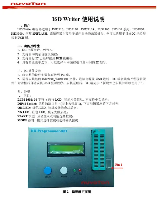
四、外观1、正面:LCM 1602: 16字符x两行LCD, 显示相关信息, 不支持中文显示;DIP48 Socket:芯片的缺口向上(左上为管脚1), 下方与锁紧座的下方对齐;OK LED:绿色LED, 待机或烧录成功后亮;NG LED:红色LED, 烧录失败后亮;START按键: 启动烧录或功能选择按键;MODE按键: 模式选择按键或选择确认按键。
Pin 1 图1 编程器正面图48PIN Socket座引脚说明:如图1所示,Socket座的第一引脚在右下脚位置,以下是引脚说明:引脚号引脚说明功能介绍1 MISO_21/CS_F/VCCA_15C MISO_21:ISD21系列SPI通讯MISO引脚;CS_F:华邦SPIFLASH片选CS引脚;VCCA_15C:ISD151系列VCCA电源输入引脚;2 SCLK_21/DO_F/VSSA15C SCLK_21:ISD21系列SPI 时钟输入引脚;DO_F:华邦SPIFLASH数据输出引脚DO;VSSA15C:ISD151系列VSSA电源模拟地输入引脚;3 SSB_21/WP_F SSB_21:ISD21系列SPI片选SSB引脚;WP_F:华邦SPIFLASH写保护输入引脚WP;4 MOSI_21/GND_F MOSI_21:ISD21系列SPI通讯MOSI引脚;GND_F:华邦SPIFLASH底线输入引脚GND;5 VSSD_21 VSSD_21:ISD21系列电源地VSSD输入引脚;14 VCCD ISD151系列数字电源VCCD输入引脚15 VSSD ISD151系列地线VSSD输入引脚16 VSSD ISD151系列地线VSSD输入引脚17 VCCD ISD151系列数字电源VCCD输入引脚19 MISO15C ISD151系列SPI通讯MISO引脚20 SCLK15C ISD151系列SPI通讯CLK时钟引脚21 SSB15C ISD151系列SPI通讯片选SSB引脚22 MOSI15C ISD151系列SPI通讯MOSI引脚31 INTB15C ISD151系列INTB输入引脚32 RDY15C ISD151系列RDY输出引脚33 RST15C ISD151系列RST复位引脚39 VCCD ISD151系列电源引脚VCCD40 VCCD ISD151系列电源引脚VCCD44 VCCP_21 ISD21系列电源引脚VCCP45 INTB_21/DI_F INTB_21:ISD21系列INTB中断引脚;DI_F:华邦SPIFLASH输入引脚46 RDY_21/SCLK_F RDY_21:ISD21系列的RDY输出引脚SCLK_F:华邦SPIFLASH时钟输入引脚47 VCCD_21/HOLD VCCD_21:ISD21系列的电源输入引脚VCCDHOLD:华邦SPIFLASH保持HOLD输入引脚48 VCC_F 华邦SPIFLASH电源输入引脚VCC注:表格中引脚号中间没有标出连续的pin脚号表示没用到。

ISD 1700系列数码语音电路使用手册(中文版)前言ISD1700系列是华邦公司新推出的语音芯片,用来替代已经停产的ISD1400系列及ISD2500系列芯片。
ISD1700系列不仅在录音时间上有更多的选择(从20秒到240秒),而且在功能上继承14及25系列的所有录放功能,并增加了一些更加人性化的提示功能及对存储地址的精确操作。
根据我们经营ISD系列芯片多年的经验来看,ISD1700的音质也较14及25系列有明显的提高。
本文根据华邦公司提供的ISD1700 Design Guide Rev 1做部分翻译,适用于ISD1720,ISD1730,ISD1740,ISD1750,ISD1760,ISD1790,ISD17120,ISD17150 ,ISD17180,ISD17210,ISD17240。
我们从来不标榜权威,但一直真诚的为大家服务,希望本手册可以帮助大家解决ISD1700使用上的问题及语音方案上的一些难题。
您也可以登陆中青论坛/bbs,或许可以找到您要的答案,也可以和其他工程师做一些交流,得到更好的方案。
如有纰漏,欢迎批评指正!目录一、特点: (3)二、电特性: (3)三、独立按键工作模式 (4)四管脚功能说明: (8)五ISD1730的SPI模式 (12)5.1 微机接口 (12)5.2 SPI 协议总述 (12)5.3 SPI处理的格式 (13)5.3.1 MOSI 数据格式 (13)5.3.2 MISO数据格式 (15)5.4 SPI协议格式 (16)5.4.1 SPI命令总览: (16)5.4.2 ISD1700芯片内部寄存器 (17)六ISD1700的存储结构 (23)七ISD1700S典型应用电路 (25)ISD1700系列多段语音录放芯片ISD1700系列芯片是华邦公司新推出的单片优质语音录放电路,该芯片提供多项新功能,包括内置专利的多信息管理系统,新信息提示(vAlert),双运作模式(独立&嵌入式),以及可定制的信息操作指示音效。
