
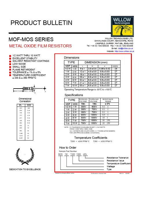
MOS6WT350100K中文资料
- 格式:pdf
- 大小:87.48 KB
- 文档页数:2

三极管参数中文与英文对照(精)电阻模型参数R 电阻倍率因子TC1 线性温度系数TC2 二次温度系数电容模型参数C 电容倍率因子VC1 线性电压系数VC2 二次电压系数TC1 线性温度系数TC2 二次温度系数电感模型参数L 电感倍率因子IL1 线性电流系数IL2 二次电流系数TC1 线性温度系数TC2 二次温度系数二极管模型参数IS 饱和电流RS 寄生串联电阻N 发射系数TT 渡越时间CJO 零偏压 PN 结电容VJ PN 结自建电势M PN 结剃度因子EG 禁带宽度XT1 IS 的温度指数FC 正偏耗尽层电容系数BV 反向击穿电压(漆点电压 IBV 反向击穿电流(漆点电流 KF 闪烁躁声系数AF 闪烁躁声指数双极晶体管(三极管IS 传输饱和电流EG 禁带宽度XTI (PT IS 的温度效应指数 BF 正向电流放大系数NF 正向电流发射系数V AF (V A 正向欧拉电压IKF (IK 正向漆点电流ISE (C2 B-E 漏饱和电流NE B-E 漏饱和电流BR 反向电流放大系数NR 反向电流发射系数V AR (VB 正想欧拉电压IKR 反向漆点电流ISC C4 B-C 漏饱和电流NC B-C 漏发射系数RB 零偏压基极电阻IRB 基极电阻降致 RBM/2时的电流RE 发射区串联电阻RC 集电极电阻CJE 零偏发射结 PN 结电容VJE PE 发射结内建电势MJE ME 集电结剃度因子CJC 零偏衬底结 PN 结电容VJC PC 集电结内建电势MJC MC 集电结剃度因子XCJC Cbe 接至内部 Rb 的内部CJS CCS 零偏衬底结 PN 结电容VJS PS 衬底结构 PN 结电容MJS MS 衬底结剃度因子FC 正偏势垒电容系数TF 正向渡越时间XTF TF 随偏置变化的系数VTF TF 随 VBC 变化的电压参数ITF 影响 TF 的大电流参数PTF 在 F=1/(2派 TF Hz 时超前相移 TR 反向渡越时间XTB BF 和 BR 的温度系数KF I/F躁声系数AF I/F躁声指数Is=14.34f 反向饱和电流。
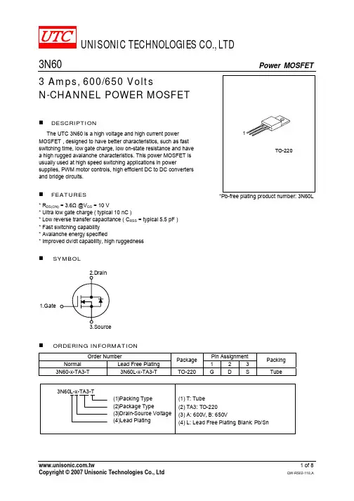
UNISONIC TECHNOLOGIES CO., LTD3N60 Power MOSFET3 Amps, 600/650 VoltsN-CHANNEL POWER MOSFETDESCRIPTIONThe UTC 3N60 is a high voltage and high current power MOSFET , designed to have better characteristics, such as fast switching time, low gate charge, low on-state resistance and have a high rugged avalanche characteristics. This power MOSFET is usually used at high speed switching applications in powersupplies, PWM motor controls, high efficient DC to DC converters and bridge circuits.FEATURES* R DS(ON)= 3.6Ω @V GS = 10 V* Ultra low gate charge ( typical 10 nC )* Low reverse transfer capacitance ( C RSS = typical 5.5 pF ) * Fast switching capability * Avalanche energy specified* Improved dv/dt capability, high ruggednessSYMBOL1.Gate*Pb-free plating product number: 3N60LORDERING INFORMATIONOrder NumberPin AssignmentNormal Lead Free Plating Package1 2 3Packing3N60-x-TA3-T 3N60L-x-TA3-TTO-220 G D S TubeABSOLUTE MAXIMUM RATINGS (T C = 25℃, unless otherwise specified)PARAMETER SYMBOL RATINGS UNIT3N60-A 600 VDrain-Source Voltage 3N60-B V DSS650 VGate-Source Voltage V GSS ±30 V Avalanche Current - (Note 1) I AR 3.0 AT C = 25°C 3.0 AContinuous Drain Current T C = 100°C I D1.9 APulsed Drain Current, T P Limited by T JMAX - (Note 1) I DM 12 A Avalanche Energy, Single Pulsed (Note 2) E AS 200 mJ Avalanche Energy, Repetitive, Limited by T JMAX E AR 7.5 mJ Peak Diode Recovery dv/dt (Note 3) dv/dt 4.5 V/ns Power Dissipation P D 75 W Junction Temperature T J +150 Storage Temperature T STG -55 ~ +150Note: Absolute maximum ratings are those values beyond which the device could be permanently damaged.Absolute maximum ratings are stress ratings only and functional device operation is not implied.THERMAL DATAPARAMETER SYMBOL TYP MAX UNITJunction-to-Case θJC 1.67 °C/W Junction-to-Ambient θJA 62.5 °C/WELECTRICAL CHARACTERISTICS (T C =25℃, unless otherwise specified)PARAMETER SYMBOL TEST CONDITIONS MIN TYP MAX UNIT Off Characteristics3N60-A 600 VDrain-Source Breakdown Voltage 3N60-B BV DSS V GS = 0 V, I D = 250 µA650 VV DS = 600 V, V GS = 0 V 10µADrain-Source Leakage Current I DSSV DS = 480 V, T C = 125°C 100µAForward V GS = 30 V, V DS = 0 V 100nAGate-Source Leakage Current Reverse I GSSV GS = -30 V, V DS = 0 V -100nABreakdown Voltage TemperatureCoefficientBV DSS /△T J I D = 250 µA, Referenced to 25°C 0.6 V/On Characteristics Gate Threshold Voltage V GS(TH) V DS = V GS , I D = 250 µA 2.0 4.0V Drain-Source On-State Resistance R DS(ON) V GS = 10 V, I D = 1.5A 2.8 3.6ΩDynamic Characteristics Input Capacitance C ISS 350 450pFOutput Capacitance C OSS 50 65pFReverse Transfer Capacitance C RSSV DS = 25 V, V GS = 0 V, f = 1MHz 5.5 7.5pF Switching Characteristics Turn-On Delay Time t D(ON) 10 30ns Turn-On Rise Time t R 30 70ns Turn-Off Delay Time t D(OFF) 20 50nsTurn-Off Fall Time t FV DD = 300V, I D = 3.0 A, R G = 25Ω(Note 4, 5) 30 70ns Total Gate Charge Q G 10 13nCGate-Source Charge Q GS 2.7 nCGate-Drain Charge Q DDV DS = 480V,I D = 3.0A, V GS = 10 V(Note 4, 5)4.9 nCELECTRICAL CHARACTERISTICS(Cont.)PARAMETER SYMBOL TEST CONDITIONS MIN TYP MAX UNITSource- Drain Diode Ratings and Characteristics Drain-Source Diode Forward Voltage V SD V GS = 0 V, I S = 3.0 A 1.4VMaximum Continuous Drain-SourceDiode Forward CurrentI S 3.0AMaximum Pulsed Drain-Source DiodeForward CurrentI SM 12AReverse Recovery Time t RR 210 ns Reverse Recovery Charge Q RR V GS = 0 V, I S = 3.0 A,dI F /dt = 100 A/µs (Note 4) 1.2 µCNotes: 1. Repetitive Rating : Pulse width limited by T J2. L = 40mH, I AS =3.0A, V DD = 50V, R G = 25 Ω, Starting T J = 25°C 3. I SD ≤ 3.0A, di/dt ≤200A/µs, V DD ≤ BV DSS , Starting T J = 25°C4. Pulse Test: Pulse width ≤ 300µs, Duty cycle ≤ 2%5. Essentially independent of operating temperatureTEST CIRCUITS AND WAVEFORMSV DDV GS (Driver)I SD (D.U.T.)Body DiodeForward Voltage DropV DS(D.U.T.)Fig. 1A Peak Diode Recovery dv/dt Test CircuitFig. 1B Peak Diode Recovery dv/dt WaveformsTEST CIRCUITS AND WAVEFORMS (Cont.)R LDDV DS90%10%V GStFig. 2A Switching Test Circuit Fig. 2B Switching WaveformsFig. 3A Gate Charge Test CircuitFig. 3B Gate Charge Waveform10VLV DDI ASFig. 4A Unclamped Inductive Switching Test Circuit Fig. 4B Unclamped Inductive Switching WaveformsTYPICAL CHARACTERISTICSD r a i n -S o u r c e B r e a k d o w n V o l t a g e , B V D S S (N o r m a l i z e d )Junction Temperature , T J (℃)1.21.11.00.90.8Breakdown Voltage Variation vs .Junction Temperature-100D r a i n -S o u r c e O n -R e s i s t a n c e , R D S (O N ) (N o r m a l i z e d )Junction Temperature , T J (℃)-50502001001503.002.01.00.50.01.52.5On-Resistance V ariation vs.Junction Temperature1010.1Drain -Source Voltage , V DS (V)D r a i n C u r r e n t , I D (A )1001011000Maximum Safe Operating AreaD r a i n C u r r e nt , I D (A )Case Temperature , T C (℃)75100012550251.01.52.02.53.0Maximum Drain Current vs .Case Temperature0.5150101Drain-to-Source Voltage , V DS (V)D r a i n C u r r e n t , I D (A )On-State Characteristics0.1Gate-Source Voltage , V GS (V)D r a i n C u r r e n t , I D (A )Transfer Characteristics1010.1TYPICAL CHARACTERISTICS(Cont.)D r a i n -S o u r c e O n -R e s i s t a n c e , R D S (O N ) (Ω)Drain Current , I D (A)12456On-Resistance Variation vs .Drain Current and Gate Voltage310.10.2Source-Drain Voltage , V SD (V)R e v e r s e D r a i n C u r r e n t , I D R (A )On State Current vs.Allowable Case Temperature 1.80.40.60.81.01.2 1.61.4106000Drain-SourceVoltage , V DS (V)C a p a c i t a n c e (p F )Capacitance Characteristics(Non-Repetitive )G a t e -S o u r c e V o l t a g e , V G S (V )Total Gate Charge , Q G (nC)26108101246420Gate Charge CharacteristicsT h e r m a l R e s p o n s e , θJ C (t )101010101010101Square Wave Pulse Duration , t 1(sec)Transient Thermal Response Curve。


6W isolated DC-DC converter in DIP package ultrawideinput and regulated single outputPatent Protection RoHSFEATURES●Ultra wide 4:1input voltage range ●High efficiency up to 85%●No-load power consumption as low as 0.12W ●Reinforced isolation,I/O isolation test voltage:6KVDC and 2MOPP high isolation●Leakage current <5µA,under 240VAC/60Hz operating conditions●Transformer creepage distance is 8mm,transformer clearance is 5mm●Operating ambient temperature range:-40℃to +85℃●Input under-voltage protection,output short circuit,over-current,over–voltage protection●EN60601-1(3rd edition medical grade)approved,EN60601-1:2006+A1:2013●Industry standard pin-outURH_P-6WR3series of isolated 6W DC-DC converter products with an ultra wide input voltage range of 9-36VDC,18-75VDC,input to output isolation is tested with 6000VDC,output over-voltage protection and output short circuit protection,EN60601-1approval;they are widely used in applications that requiring high isolation,such as medical,electricity,also for energy storage systems that requiring an low no-load power consumption.Hot Plug UnavailableImmunitySurgeIEC/EN61000-4-5±2KV (see Fig.3-①for recommended circuit)perf.Criteria B CSIEC/EN61000-4-63Vr.m.sperf.Criteria A Immunities of voltage dip,drop and short interruptionIEC/EN61000-4-290-70%perf.Criteria BOperating Temperature()℃Temperature Derating CurveO u t p u t P o w e r P e r c e n t (%)-400407185120020406080100120Fig.1Design Reference1.Typical applicationAll the DC/DC converters of this series are tested before delivery using the recommended circuit shown in Fig.2.Input and/or output ripple can be further reduced by appropriately increasing theinput &output capacitor values Cin and Cout and/or by selecting capacitors with a low ESR (equivalent series resistance).Also make sure that the capacitance is not exceeding the specified max.capacitive load value of the product.VinGND0VFig.2Vin Cin Cout 24VDC 100uF 10µF 48VDC10µF -47µF10µF914192429343618243036424854606675Operating Temperature (℃)2.EMC solution-recommended circuitFig.3Notes:For EMC tests we use part ①in Fig.3for immunity and part ②foremissions test.Selecting based on needs.Parameter description :Model Vin:24V Vin:48V FUSE Choose according to actual input currentMOV S20K30S14K60C0,C4330µF/50V 330µF/100VC1,C210µF/50V --C3Refer to the Cout in Fig.2LDM110µH --CY1,CY21nF/6KV--3.The products do not support parallel connection of their output4.For additional information please refer to DC-DC converter application notes on Note:Unit :mm[inch]Pin diameter tolerances :±0.10[±0.004]General tolerances:±0.50[±0.020]Note:Grid 2.54*2.54mmTHIRD ANGLE PROJECTIONNote:1.For additional information on Product Packaging please refer to .The Packaging bag number of Horizontalpackage:58210008;2.The maximum capacitive load offered were tested at nominal input voltage range and full load;3.Unless otherwise specified,parameters in this datasheet were measured under the conditions of Ta=25℃,humidity<75%RH with nominalinput voltage and rated output load;4.All index testing methods in this datasheet are based on our company corporate standards;5.The performance indexes of the product models listed in this datasheet are as above,but some indexes of non-standard modelproducts will exceed the above-mentioned requirements,and please contact our technicians directly for specific information;6.We can provide product customization service;7.Products are related to laws and regulations:see"Features"and"EMC";8.Our products shall be classified according to ISO14001and related environmental laws and regulations,and shall be handled byqualified units.Mornsun Guangzhou Science&Technology Co.,Ltd.Address:No.5,Kehui St.1,Kehui Development Center,Science Ave.,Guangzhou Science City,Huangpu District,Guangzhou,P.R.China Tel:86-20-38601850Fax:86-20-38601272E-mail:***************。