COMSOL光学案例
- 格式:pdf
- 大小:1.17 MB
- 文档页数:16

comsol 案例COMSOL(Computation Method for Science and Engineering)是一种用于多物理场问题建模和模拟的软件平台。
以下将介绍一个使用COMSOL的案例。
在某一电子设备生产厂家中,有一个问题需要解决:在电子元器件的生产过程中,需要将组件加热至一定温度,以便进行焊接等工艺。
然而,由于加热方式不当,过高的温度可能会导致电子元器件受损。
因此,厂家希望通过使用COMSOL软件来优化加热过程,以保证元器件的安全性。
首先,使用COMSOL建立了一个三维模型,包括了电子元器件和加热设备。
在模型中,定义了材料的热传导系数、热容量和密度等参数。
根据要求的加热温度,设置了加热设备的功率。
模型还考虑了元器件周围的导热情况,包括传导、对流和辐射。
然后,通过COMSOL进行模拟计算。
COMSOL利用有限元方法进行求解,将模型划分为多个小单元,计算出每个单元的温度分布。
通过迭代计算,最终得到整个模型在加热过程中的温度变化情况。
根据模拟结果,厂家可以优化加热过程。
例如,他们可以根据元器件的特性和要求的加热温度,调整加热设备的功率大小,以及加热设备和元器件之间的距离。
他们还可以通过改变元器件的材料和结构,来提高热传导性能,减少温度梯度。
通过使用COMSOL进行模拟和优化,厂家成功地解决了元器件加热过程中的温度控制问题。
他们能够确保元器件在安全温度范围内进行加热,避免了因过高温度导致的损坏。
此外,优化后的加热过程还能够提高元器件的生产效率和质量,降低生产成本。
综上所述,COMSOL软件在电子元器件加热过程的优化中发挥了关键作用。
它通过建立和求解多物理场模型,帮助厂家实现了对加热过程的精确控制,提高了产品的质量和性能。

COMSOL光学案例Case Study 1: Refractive Index Sensing using a MicrocavityOptical sensors are widely used in various applications, including biomedical, environmental, and industrial fields. One important characteristic of optical sensors is their sensitivity to changes in refractive index. In this case study, we will simulate a microresonator-based refractive index sensor using COMSOL.A cylindrical microcavity is considered with a highrefractive index material surrounded by a low refractive index medium. The refractive index of the surrounding medium is varied, and the transmission spectrum of the microcavity is calculated using the COMSOL Electromagnetic Waves Module.The simulation setup includes a 2D model of the microcavity with a defined geometry and material properties. The material properties include the refractive index, which can be assignedas a constant value or wavelength-dependent using experimental data. The surrounding medium is defined by changing therefractive index value.After the simulation, the transmission spectrum of the microcavity is obtained. By analyzing the spectrum, we can observe the shift in the resonant frequency or wavelength as the refractive index of the surrounding medium changes. This shiftcan be used to determine the refractive index of an unknown sample, making the microresonator a sensitive refractive index sensor.Case Study 2: Design of a Grating Coupler for Efficient Light CouplingGrating couplers are essential devices in integrated optics for efficient coupling of light between waveguides and free space. In this case study, we will design a grating coupler using COMSOL to achieve high coupling efficiency.The design process involves optimizing the grating period, duty cycle, grating height, and refractive index contrast between the grating material and the surrounding medium. The goal is to maximize the coupling efficiency by enhancing the diffraction of light into the desired waveguide mode.COMSOL provides a powerful tool called the Optimization Module, which can be used to automate and streamline the design optimization process. The module allows users to defineobjective functions, design variables, and constraints for the optimization problem. The optimization algorithm then searches for the optimum solution by iteratively adjusting the design variables.In this case study, the design variables include the grating period, duty cycle, and grating height. The objective functionis defined as the maximum coupling efficiency, and constraints can be set to limit the range of values for the design variables.After the optimization process, the final design parameters are obtained, which can be used to fabricate the grating coupler. COMSOL provides post-processing tools to visualize the electric field distribution, power coupling, and other relevantparameters of the optimized design.ConclusionCOMSOL is a powerful and versatile simulation tool for modeling and analyzing optical systems. The two case studies discussed here demonstrate the capabilities of COMSOL in simulating refractive index sensing and grating coupler design. With its extensive range of modules and features, COMSOL enables researchers and engineers to explore and optimize variousoptical devices and systems.。


Comsol经典实例012: 高斯波速的二次谐波产生激光系统是现代电子技术中的一个重要应用领域。
激光束的生成方法有很多种, 这些方法有个共同点: 波长由受激发射决定, 而受激发射取决于材料参数。
通常很难生成具有短波长的激光。
但是, 如果使用非线性材料, 就有可能产生频率为激光频率数倍的谐波。
通过使用二阶非线性材料可生成波长为基频光束波长一半的相干光。
本案例演示了如何设置非线性材料属性, 通过瞬态波仿真产生二次谐波。
模型中一束波长为1.06μm的激光聚焦于非线性晶体, 光束的腰部落于晶体内。
在激光的传播过程中, 大部分能量都集中在传播轴附近, 在求解麦克斯韦方程时可以近轴近似, 由此获得高斯波束。
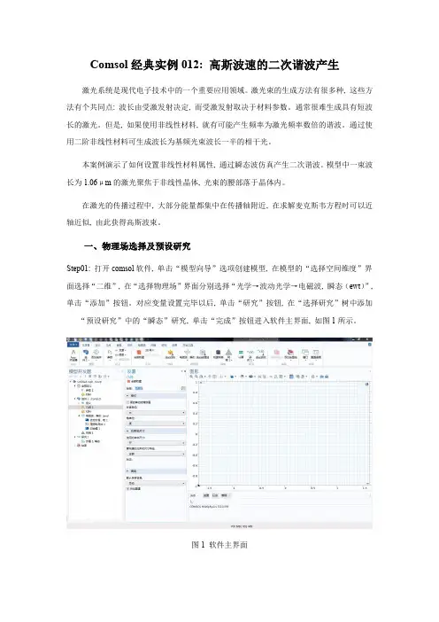
一、物理场选择及预设研究Step01: 打开comsol软件, 单击“模型向导”选项创建模型, 在模型的“选择空间维度”界面选择“二维”, 在“选择物理场”界面分别选择“光学→波动光学→电磁波, 瞬态(ewt)”, 单击“添加”按钮。
对应变量设置完毕以后, 单击“研究”按钮, 在“选择研究”树中添加“预设研究”中的“瞬态”研究, 单击“完成”按钮进入软件主界面, 如图1所示。
图1 软件主界面二、全局定义1.参数Step02: 参数设置。
在模型开发器窗口的全局定义节点下, 单击“参数”子节点, 在“参数”设置窗口中, 定位到“参数”栏, 输入如图2所示的参数。
图2 设置全局参数2.解析定义Step03: 在“主屏幕”工具栏中单击“函数”选项, 在下拉菜单中选择“全局→解析”选项。
单击“解析1”子节点, 在“解析”设置窗口中, 定位到“函数名称”栏, 在文本输入框中输入“w”;定位到“定义”栏, 在“表达式”文本输入框中输入“w0*sqrt(1+(x/x)^2)”;定位到“单位”栏, 在“变元”文本输入框中输入“m”, 在“函数”在文本输入框中输入“m”,如图3所示。
Step04:在“主屏幕”工具栏中单击“函数”选项, 在下拉菜单中选择“全局→解析”选项。

COMSOL⼆维膜层光学性能-吸收率仿真教学COMSOL⼆维膜层结构光学性能/吸收率仿真教学新建
1. 新建→模型向导→⼆维;
2. →选择物理场:光学→波动光学→电磁波,频域→增加→研究;
3. 选择研究:波长域→完成;
建模
4. ⼏何绘制多个长⽅形形成多层膜结构;
5. 必要的情况下可以在上下层加⼊空⽓层(真空层);
边界条件
6. 添加“端⼝”,设置红外⼊射端⼝,在空⽓层边界上。
再添加“端⼝”,设置出射端⼝,另⼀端的空⽓层;
7. 模型两侧边界设置为“周期性边界条件”;
8. 对于膜层很薄的部分,可以设置为“过渡边界条件”,代替超薄层,厚度可在此条件下设置;
9. 进⾏⽹格化;
材料参数
10. 顶部⼯具栏:增加材料;
11. 可在右侧框内搜索要添加的材料,然后“增加到选择”;或者添加空材料,去选择⼀个域,然后材料属性⽬录下会出现做该仿真必要的参数,输⼊参数即可;研究:结果
12. 研究→波长域,设置波长范围及步长,点击“研究”;
13. 派⽣值→全局计算,表达式选“ewfd.Atotal” ;数据系列运算选“⽆”,计算;仿真图下⽅出现“表格”,得到“波长”与“吸收率”关系。
点击“表图”按钮,得到“吸收曲线”;
14. 派⽣值→全局计算,表达式选“ewfd.Atotal”;数据系列运算选“平均值”,计算;仿真图下⽅出现“表格”,得到“平均吸收率”值。

comsol学习案例篇一:COMSOL寻找最小曲面案例COMSOL寻找最小曲面案例觉得这个例子有点。
参考《COMSOLMulitiphyic基本操作指南和常见问题解答》P71问题提出:给定一个空间曲线,通过这条曲线的曲面有无数个,那么哪个曲面的面积最小呢?数学处理:曲线在某Y平面上有一个投影,在这个投影区域Ω的边界Ω上给定函数值u|Ω=Φ(某,y),则曲面的最小面积为:采用Euler-Lagrange方程,上式转化为:变分法:采用试函数法求解该问题为:相当于输入:引入边界条件:u|Ω=Φ(某,y)即可求解。
这个算例告诉我们如何求解最小值问题,如果用COMSOL的弱形式,那么只须将求解函数丢到tet()中,加上合适的边界条件即可。
求解设置:引入边界条件:取Ω={(某,y)|某^2+y^2<1},u|Ω=某^2。
即求解域为一个半径为1的圆,边界值用dirichlet条件r=某^2,其空间曲线为一个马鞍线,解的边缘为该曲线,而显示的曲面为最小面积的曲面。
另外的例子:矩形求解域,边界值为(某-0.5)^2+(y-0.5)^2氯碱薄膜电池总结本描述氯碱薄膜电池中阳极和阴极结构上的二次电流分布。
模拟了整个电池中的一个单元。
目录1.全局定义............................................................. ............................................................... . (3)1.1.参数1.............................................................. ............................................................... (3)2.1.2.2.2.3.定义............................................................. ............................................................................4Geometry1........................................ ............................................................... .......................4材料............................................................. ............................................................... . (5)2.4.SecondaryCurrentDitribution................................ (7)2.5.Meh1....................................................... ............................................................... . (21)3.Study1....................................................... ............................................................... (24)3.1.Stationary................................................. ............................................................... .. (24)3.2.求解器配置............................................................. .. (2)44.Reult........................................................ ............................................................... .. (26)4.1.DataSet.................................................... ............................................................... . (26)4.2.DerivedValue............................................... ............................................................... (26)4.3.Table...................................................... ............................................................... . (27)4.4.绘图组............................................................. ............................................................... . (27)1全局定义全局设定使用的模块1.1参数1参数组件设定2.1定义2.1.1坐标系BoundarySytem1坐标名称2.2Geometry1Geometry1单位几何统计2.2.1Import1(imp1)设定2.3材料2.3.1Material1Material1选择材料参数篇三:COMSOL核心技术与应用中国管理科学研究院人才战略研究所人才所[2022]第(25)号关于举办“COMSOL多物理场耦合核心技术与应用”高级培训通知1、本次培训采取深入浅出的授课方法,先以简单的案例引入分析仿真的基本原理,随后重点讲解多种常用单元的功能和特性,以及有COMSOL的实用技术和处理方法,紧密结合应用实例,针对工作中存在的疑难问题进行分析讲解和专题讨论,有效提升学员解决复杂问题的能力。

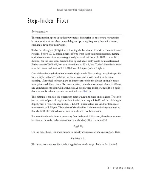
Step-Index FiberIntroductionThe transmission speed of optical waveguides is superior to microwave waveguides because optical devices have a much higher operating frequency than microwaves, enabling a far higher bandwidth.Today the silica glass (SiO 2) fiber is forming the backbone of modern communication systems. Before 1970, optical fibers suffered from large transmission losses, making optical communication technology merely an academic issue. In 1970, researchers showed, for the first time, that low-loss optical fibers really could be manufactured. Earlier losses of 2000 dB/km now went down to 20 dB/km. Today’s fibers have losses near the theoretical limit of 0.16 dB/km at 1.55 μm (infrared light).One of the winning devices has been the single-mode fiber, having a step-index profile with a higher refractive index in the center core and a lower index in the outer cladding. Numerical software plays an important role in the design of single-mode waveguides and fibers. For a fiber cross section, even the most simple shape is difficult and cumbersome to deal with analytically. A circular step-index waveguide is a basic shape where benchmark results are available (see Ref. 1).This example is a model of a single step-index waveguide made of silica glass. The inner core is made of pure silica glass with refractive index n 1 = 1.4457 and the cladding is doped, with a refractive index of n 2 = 1.4378. These values are valid for free-space wavelengths of 1.55 μm. The radius of the cladding is chosen to be large enough so that the field of confined modes is zero at the exterior boundaries.For a confined mode there is no energy flow in the radial direction, thus the wave must be evanescent in the radial direction in the cladding. This is true only ifOn the other hand, the wave cannot be radially evanescent in the core region. ThusThe waves are more confined when n eff is close to the upper limit in this interval.n eff n 2>n 2n eff n 1<<Model DefinitionThe mode analysis is made on a cross-section in the xy -plane of the fiber. The wave propagates in the z direction and has the formwhere ω is the angular frequency and β the propagation constant. An eigenvalue equation for the electric field E is derived from Helmholtz equationwhich is solved for the eigenvalue λ = −j β.As boundary condition along the outside of the cladding the electric field is set to zero. Because the amplitude of the field decays rapidly as a function of the radius of the cladding this is a valid boundary condition.Results and DiscussionWhen studying the characteristics of optical waveguides, the effective mode index of a confined mode,as a function of the frequency is an important characteristic. A common notion is the normalized frequency for a fiber. This is defined aswhere a is the radius of the core of the fiber. For this simulation, the effective mode index for the fundamental mode, 1.4444 corresponds to a normalized frequency of4.895. The electric and magnetic fields for this mode is shown in Figure 1 below.E x y z t ,,,()E x y ,()e j ωt βz –()=∇∇E ×()×k 02n 2E –0=n eff βk 0-----=V 2πa λ0----------n 12n 22–k 0a n 12n 22–==Figure 1: The surface plot visualizes the z component of the electric field. This plot is for the effective mode index 1.4444.Reference1. A. Yariv, Optical Electronics in Modern Communications, 5th ed., Oxford University Press, 1997.Model Library path: RF_Module/Tutorial_Models/step_index_fiberModeling InstructionsFrom the File menu, choose New.N E W1In the New window, click Model Wizard.M O D E L W I Z A R D1In the Model Wizard window, click 2D.2In the Select physics tree, select Radio Frequency>Electromagnetic Waves, Frequency Domain (emw).3Click Add.4Click Study.5In the Select study tree, select Preset Studies>Mode Analysis.6Click Done.G E O M E T R Y11In the Model Builder window, under Component 1 (comp1) click Geometry 1.2In the Settings window for Geometry, locate the Units section.3From the Length unit list, choose µm.Circle 1 (c1)1On the Geometry toolbar, click Primitives and choose Circle.2In the Settings window for Circle, locate the Size and Shape section.3In the Radius text field, type 40.4Click the Build Selected button.Circle 2 (c2)1On the Geometry toolbar, click Primitives and choose Circle.2In the Settings window for Circle, locate the Size and Shape section.3In the Radius text field, type 8.4Click the Build Selected button.M A T E R I A L SMaterial 1 (mat1)1In the Model Builder window, under Component 1 (comp1) right-click Materials and choose Blank Material.2Right-click Material 1 (mat1) and choose Rename.3In the Rename Material dialog box, type Doped Silica Glass in the New label text field.4Click OK.5Select Domain 2 only.6In the Settings window for Material, click to expand the Material properties section. 7Locate the Material Properties section. In the Material properties tree, select Electromagnetic Models>Refractive Index>Refractive index (n).8Click Add to Material.9Locate the Material Contents section. In the table, enter the following settings:Property Name Value Unit Property groupRefractive index n 1.44571Refractive indexMaterial 2 (mat2)1In the Model Builder window, right-click Materials and choose Blank Material.2Right-click Material 2 (mat2) and choose Rename.3In the Rename Material dialog box, type Silica Glass in the New label text field. 4Click OK.5Select Domain 1 only.6In the Settings window for Material, click to expand the Material properties section. 7Locate the Material Properties section. In the Material properties tree, select Electromagnetic Models>Refractive Index>Refractive index (n).8Click Add to Material.9Locate the Material Contents section. In the table, enter the following settings:Property Name Value Unit Property groupRefractive index n 1.43781Refractive indexE L E C T R O M A G N E T I C W A V E S,F R E Q U E N C Y D O M A I N(E M W)Wave Equation, Electric 11In the Model Builder window, expand the Component 1 (comp1)>Electromagnetic Waves, Frequency Domain (emw) node, then click Wave Equation, Electric 1.2In the Settings window for Wave Equation, Electric, locate the Electric Displacement Field section.3From the Electric displacement field model list, choose Refractive index.M E S H11In the Model Builder window, under Component 1 (comp1) click Mesh 1.2In the Settings window for Mesh, locate the Mesh Settings section.3From the Element size list, choose Finer.4Click the Build All button.S T U D Y1Step 1: Mode Analysis1In the Model Builder window, under Study 1 click Step 1: Mode Analysis.2In the Settings window for Mode Analysis, locate the Study Settings section.3In the Search for modes around text field, type 1.446. The modes of interest have an effective mode index somewhere between the refractive indices of the two materials. The fundamental mode has the highest index. Therefore, setting the mode index to search around to something just above the core index guarantees that the solver will find the fundamental mode.4In the Mode analysis frequency text field, type c_const/1.55[um]. This frequency corresponds to a free space wavelength of 1.55 μm.5On the Model toolbar, click Compute.R E S U L T SElectric Field (emw)1Click the Zoom Extents button on the Graphics toolbar.2Click the Zoom In button on the Graphics toolbar.3The default plot shows the distribution of the norm of the electric field for the highest of the 6 computed modes (the one with the lowest effective mode index).To study the fundamental mode, choose the highest mode index. Because the magnetic field is exactly 90 degrees out of phase with the electric field you can see both the magnetic and the electric field distributions by plotting the solution at a phase angle of 45 degrees.Data Sets1In the Model Builder window, expand the Results>Data Sets node, then click Study 1/ Solution 1.2In the Settings window for Solution, locate the Solution section.3In the Solution at angle (phase) text field, type 45.Electric Field (emw)1In the Model Builder window, under Results click Electric Field (emw).2In the Settings window for 2D Plot Group, locate the Data section.3From the Effective mode index list, choose 1.4444 (2).4In the Model Builder window, expand the Electric Field (emw) node, then click Surface 1.5In the Settings window for Surface, click Replace Expression in the upper-right corner of the Expression section. From the menu, choose Model>Component1>Electromagnetic Waves, Frequency Domain>Electric>Electric field>emw.Ez - Electricfield, z component.6On the 2D plot group toolbar, click Plot.Add a contour plot of the H-field.7In the Model Builder window, right-click Electric Field (emw) and choose Contour.8In the Settings window for Contour, click Replace Expression in the upper-right corner of the Expression section. From the menu, choose Model>Component1>Electromagnetic Waves, Frequency Domain>Magnetic>Magnetic field>emw.Hz -Magnetic field, z component.9On the 2D plot group toolbar, click Plot. The distribution of the transversal E and H field components confirms that this is the HE11 mode. Compare the resulting plot with that in Figure 1.。

Modeling of Pyramidal Absorbers for an Anechoic ChamberIntroductionIn this example, a microwave absorber is constructed from an infinite 2D array of pyramidal lossy structures. Pyramidal absorbers with radiation-absorbent material (RAM) are commonly used in anechoic chambers for electromagnetic wavemeasurements. Microwave absorption is modeled using a lossy material to imitate the electromagnetic properties of conductive carbon-loaded foam.Perfectly matched layersPortConductive pyramidal formUnit cell surrounded by periodic conditionsConductive coating on the bottomFigure 1: An infinite 2D array of pyramidal absorbers is modeled using periodic boundary conditions on the sides of one unit cell.Model DefinitionThe infinite 2D array of pyramidal structures is modeled using one unit cell with Floquet-periodic boundary conditions on four sides, as shown in Figure 1. Thegeometry of one unit cell consists of one pyramid sitting on a block made of the samematerial. There are perfectly matched layers (PMLs) above the pyramid and the remaining space between the pyramid and the PMLs is filled with air.The pyramidal absorber is made of a conductive material (σ = 0.5 S/m). At the interface of the conductive material and air, the incident field is partially reflected and partially transmitted into the pyramid. The transmitted field is attenuated inside of the lossy material. For angles within a particular range of normal incidence, the propagation direction of the reflected field is not back towards the source, but instead towards another surface of the conductive material. The process of partial reflection and partial transmission with subsequent attenuation is repeated until the field reaches the base of the pyramid. The amplitude of the field at the base of the pyramid is drastically reduced and so the reflection from the absorber at this point is marginal. The process is illustrated in Figure 2.Incident waveConductive foamNoise from outside the chamber isblocked by a highly conductive layerFigure 2: The incident wave is partially transmitted into the conductive foam where it is subsequently attenuated. For angles within a particular range of normal incidence, the reflected component of the field propagates towards another conducting surface where the process is repeated.The bottom of the absorber has a thin highly conductive layer to block any noise from outside the anechoic chamber. Before mounting absorbers on the walls of the anechoicchamber, it is necessary to apply a conductive coating on the walls, which is modeled as a perfect electric conductor (PEC).The model domain immediately outside of the conducting foam is filled with air. Perfectly matched layers (PMLs) above the air at the top of the unit cell absorb higher order modes generated by the periodic structure − if there are any − as well as the upwards traveling excited mode from the source port. The PMLs attenuate the field in the direction perpendicular to the PML boundary. Since the model is solved for a range of incident angles, the wavelength inside the PMLs is set to 2π/|k0cosθ|, which, in some sense, is the wavelength of the normal component of the wave vector.A port boundary condition is placed on the interior boundary of the PMLs, adjacent to the air domain. The interior port boundaries with PML backing require the slit condition. The port orientation is specified to define the inward direction for theS-parameter calculation. Since higher order diffraction modes are not of particular interest in this example, the combination of Domain-backed type slit port and PMLs is used instead of adding a Diffraction order port for each diffraction order and polarization.The periodic boundary condition requires identical surface meshes on paired boundaries. An identical surface mesh can be created by using the Copy Face operation from one boundary to another boundary.Results and DiscussionFigure 3 shows the norm of the electric field and power flow in the case where the elevation angle of incidence is 30 degrees and the azimuth angle is zero. The intensity of the illuminating wave is strong near the tip of the absorber. It decreases towards the base of the pyramid, where it is ultimately very weak.The S-parameter for y-axis polarized incident waves is plotted in Figure 4. The plot shows quantitatively that the absorber performs well for a range of incident elevation angles less than 40 degrees.case where the elevation angle of incidence is 30 degrees and the azimuthal angle is zero.Figure 4: The S-parameter is plotted as a function of incident angle.Application Library path: RF_Module/Passive_Devices/pyramidal_absorberModeling InstructionsFrom the File menu, choose New.N E W1In the New window, click Model Wizard.M O D E L W I Z A R D1In the Model Wizard window, click 3D.2In the Select physics tree, select Radio Frequency>Electromagnetic Waves, Frequency Domain (emw).3Click Add.4Click Study.5In the Select study tree, select Preset Studies>Frequency Domain.6Click Done.G E O M E T R Y11In the Model Builder window, under Component 1 (comp1) click Geometry 1.2In the Settings window for Geometry, locate the Units section.3From the Length unit list, choose mm.G L O B A L D E F I N I T I O N SParameters1On the Home toolbar, click Parameters.2In the Settings window for Parameters, locate the Parameters section.3In the table, enter the following settings:Here, c_const is a predefined COMSOL constant for the speed of light in vacuum.D E F I N I T I O N SVariables 11On the Home toolbar, click Variables and choose Local Variables .2In the Settings window for Variables, locate the Variables section.3In the table, enter the following settings:G E O M E T R Y 1Block 1 (blk1)1On the Geometry toolbar, click Block .2In the Settings window for Block, locate the Size section.3In the Width text field, type 50.4In the Depth text field, type 50.5In the Height text field, type 280.6Locate the Position section. In the x text field, type -25.7In the y text field, type -25.8In the z text field, type -90.9Right-click Component 1 (comp1)>Geometry 1>Block 1 (blk1) and choose Build Selected .Name Expression ValueDescription theta 0[deg]0 rad Elevation angle phi 0[deg]0 rad Azimuth angle f05[GHz]5E9 Hz Frequency lda0c_const/f00.05996 mWavelengthNam e Expression UnitDescriptionk_0emw.k0rad/m Wavenumber, free space k_x k_0*sin(theta)*cos(phi)rad/m Wavenumber, x-component k_y k_0*sin(theta)*sin(phi)rad/m Wavenumber, y-component k_zk_0*cos(theta)rad/mWavenumber, z-component10Click the Wireframe Rendering button on the Graphics toolbar.Block 2 (blk2)1On the Geometry toolbar, click Block.2In the Settings window for Block, locate the Size section.3In the Width text field, type 50.4In the Depth text field, type 50.5In the Height text field, type 180.6Locate the Position section. From the Base list, choose Center.Block 3 (blk3)1On the Geometry toolbar, click Block.2In the Settings window for Block, locate the Size section.3In the Width text field, type 50.4In the Depth text field, type 50.5In the Height text field, type 25.6Locate the Position section. From the Base list, choose Center.7In the z text field, type -77.5.Pyramid 1 (pyr1)1On the Geometry toolbar, click More Primitives and choose Pyramid. 2In the Settings window for Pyramid, locate the Size and Shape section. 3In the Base length 1 text field, type 50.4In the Base length 2 text field, type 50.5In the Height text field, type 120.6In the Ratio text field, type 0.7Locate the Position section. In the z text field, type -65.8Click the Build All Objects button.The finished geometry should look like this.Set up the physics based on the direction of propagation and the E-field polarization. Assume a TE-polarized wave which is equivalent to s-polarization and perpendicular polarization. E x and E z are zero while E y is dominant.E L E C T R O M A G N E T I C W A V E S,F R E Q U E N C Y D O M A I N(E M W)1In the Model Builder window, under Component 1 (comp1) click Electromagnetic Waves, Frequency Domain (emw).2In the Settings window for Electromagnetic Waves, Frequency Domain, locate the Physics-Controlled Mesh section.3Select the Enable check box.Set the maximum mesh size to 0.2 wavelengths or smaller.4In the Maximum element size text field, type lda0/5.5Locate the Analysis Methodology section. From the Methodology options list, choose Fast.Periodic Condition 11On the Physics toolbar, click Boundaries and choose Periodic Condition.2Select Boundaries 1, 4, 9, and 18–20 only.3In the Settings window for Periodic Condition, locate the Periodicity Settingssection.4From the Type of periodicity list, choose Floquet periodicity .5Specify the k F vector asPeriodic Condition 21On the Physics toolbar, click Boundaries and choose Periodic Condition .k_x x k_y y 0z2Select Boundaries 2, 5, 10, 13, 14, and 16 only.3In the Settings window for Periodic Condition, locate the Periodicity Settingssection.4From the Type of periodicity list, choose Floquet periodicity .5Specify the k F vector asPort 11On the Physics toolbar, click Boundaries and choose Port .k_x x k_y y 0z2Select Boundary 11 only.3In the Settings window for Port, locate the Port Properties section.4From the Wave excitation at this port list, choose On .5Select the Activate slit condition on interior port check box.6From the Slit type list, choose Domain-backed .7From the Port orientation list, choose Reverse .8Locate the Port Mode Settings section. Specify the E 0 vector as9In the β text field, type abs(k_z).Scattering Boundary Condition 11On the Physics toolbar, click Boundaries and choose Scattering Boundary Condition .2Select Boundary 12 only.x exp(-i*k_x*x)*exp(-i*k_y*y)[V/m]y 0zM A T E R I A L SMaterial 1 (mat1)1In the Model Builder window, under Component 1 (comp1) right-click Materials andchoose Blank Material .2In the Settings window for Material, locate the Material Contents section.3In the table, enter the following settings:Material 2 (mat2)1In the Model Builder window, right-click Materials and choose Blank Material .2Select Domains 1 and 3 only.3In the Settings window for Material, locate the Material Contents section.4In the table, enter the following settings:PropertyNameValue UnitProperty groupRelative permittivity epsilonr 11Basic Relative permeability mur 11Basic Electrical conductivitysigmaS/mBasicPropertyNameValue UnitProperty groupRelative permittivity epsilonr 11BasicD E F I N I T I O N SPerfectly Matched Layer 1 (pml1)1On the Definitions toolbar, click Perfectly Matched Layer .2Select Domain 4 only.3In the Settings window for Perfectly Matched Layer, locate the Scaling section.4From the Typical wavelength from list, choose User defined .5In the Typical wavelength text field, type 2*pi/abs(k_z).Since the model is solved for a range of incident angles, the wavelength inside the PMLs is set to 2φ/|k 0cos(θ)|, which is the wavelength of the normal component of the wave vector.M E S H 1In the Model Builder window, under Component 1 (comp1) right-click Mesh 1 and choose Build All .Relative permeability mur 11Basic Electrical conductivitysigma0.5S/mBasicProperty Name Value Unit Property groupD E F I N I T I O N SView 11On the View 1 toolbar, click Hide Geometric Entities.2Select Domain 4 only.3In the Settings window for Hide Geometric Entities, locate the Geometric Entity Selection section.4From the Geometric entity level list, choose Boundary.5Select Boundaries 4, 5, 9, and 10 only.M E S H1S T U D Y1Step 1: Frequency Domain1In the Model Builder window, under Study 1 click Step 1: Frequency Domain.2In the Settings window for Frequency Domain, locate the Study Settings section. 3In the Frequencies text field, type f0.Parametric Sweep1On the Study toolbar, click Parametric Sweep.2In the Settings window for Parametric Sweep, locate the Study Settings section.3Click Add.4In the table, enter the following settings:Parameter name Parameter value list Parameter unittheta range(0[deg],5[deg],85[deg])5On the Study toolbar, click Compute.R E S U L T SData Sets1On the Results toolbar, click Selection.2In the Settings window for Selection, locate the Geometric Entity Selection section.3From the Geometric entity level list, choose Domain.4Select Domains 1–3 only.Electric Field (emw)1In the Model Builder window, expand the Results>Electric Field (emw) node, then click Multislice 1.2In the Settings window for Multislice, locate the Multiplane Data section.3Find the z-planes subsection. In the Planes text field, type 0.4In the Model Builder window, right-click Electric Field (emw) and choose Arrow Volume.5In the Settings window for Arrow Volume, click Replace Expression in the upper-right corner of the Expression section. From the menu, choose Component1>Electromagnetic Waves, Frequency Domain>Energy andpower>emw.Poavx,...,emw.Poavz - Power flow, time average.6Locate the Arrow Positioning section. Find the x grid points subsection. In the Points text field, type 21.7Find the y grid points subsection. In the Points text field, type 1.8Find the z grid points subsection. In the Points text field, type 21.9On the Electric Field (emw) toolbar, click Plot.10In the Model Builder window, click Electric Field (emw).11In the Settings window for 3D Plot Group, locate the Data section.12From the Parameter value (theta (rad)) list, choose 0.5236.13On the Electric Field (emw) toolbar, click Plot.14Click the Zoom Extents button on the Graphics toolbar.See Figure 3 to compare the plotted results.1D Plot Group 21On the Home toolbar, click Add Plot Group and choose 1D Plot Group.2On the 1D Plot Group 2 toolbar, click Global.3In the Settings window for Global, click Replace Expression in the upper-right corner of the y-axis data section. From the menu, choose Component 1>Electromagnetic Waves, Frequency Domain>Ports>emw.S11dB - S-parameter, dB, 11 component.4On the 1D Plot Group 2 toolbar, click Plot.The calculated S-parameters at the input port are shown as a function of the incident angle. Compare with that shown in Figure 4.。
Comsol经典实例011: 铜柱的感应加热铜柱中的感应电流会使铜柱的温度升高, 而温度的变化会导致铜的电导率发生变化。
该模型涉及电磁场与热场之间的相互耦合, 要准确描述次物理过程, 需要同时求解传热过程和电磁场传播。
由感应电流引起的加热称为感应加热。
由电流引起的加热称为电阻加热或欧姆加热。
感应电流加热中要解决的难题是需要对感应线圈中的大电流进行主动冷却。
采用空心的线圈导体并在其中灌入水可以实现这一目的。
也就是使流速相当低, 冷却水会形成高度发展的湍流, 在导体和流体之间进行高效传热。
本案例阐明了基于湍流和实时混合假设的水冷却简化的建模方法。
一、参数设置Step01: 打开comsol软件, 单击“模型向导”选项创建模型, 在模型的“选择空间维度”界面选择“二维轴对称”, 在“选择物理场”界面分别选择“传热→电磁热→感应加热”, 单击“添加”按钮。
对应变量设置完毕以后, 单击“研究”按钮, 在“选择研究”树中添加“所选物理场接口的预设研究”中的“频域-瞬态”研究, 单击“完成”按钮进入软件主界面, 如图1所示。
图1 软件主界面Step02: 参数设置。
在模型开发器窗口的全局定义节点下, 单击“参数”子节点, 在“参数”设置窗口中, 定位到“参数”栏, 输入如图2所示的参数。
图2 设置全局参数二、几何模型1.矩形绘制Step03: 添加第一个矩形。
右键单击“几何1”节点, 在弹出的下拉菜单中选择“矩形”, 定位到“大小和半径”栏, 在“宽度”文本输入框中输0.3, 在“高度”文本输入框中输0.4;定位到“位置”栏, 在“z”的文本输入框中输入-0.2。
单击“构建选定对象”, 如图3所示。
Step04:添加第二个矩形。
右键单击“几何1”节点, 在弹出的下拉菜单中选择“矩形”, 定位到“大小和半径”栏, 在“宽度”文本输入框中输0.02, 在“高度”文本输入框中输0.15;定位到“位置”栏, 在“z”的文本输入框中输入-0.075。
COMSOL案例electricsensor预览说明:预览图片所展示的格式为文档的源格式展示,下载源文件没有水印,内容可编辑和复制案例1:Elcectromagnetics>electric sensor背景:本案例介绍如何在盒子边界上施加电位差,来现实盒子的内部介电常数,该介电常数的差异讲产生不同的表面电流。
理论(相关方程与边界条件):静电,方程:▽·D=ρV, E=-▽V,因变量V其中D是电通量,ρ是电荷,E是电场强度,V是电势边界条件:电荷守恒1:方程:E=-▽V,▽·(ε0εr E)=ερV,D=ε0εr E,ε0为真空绝对介电常数,ε0=8.85*e-12,F/m,εr为相对介电常数,用户自定义εr=1,域1电荷守恒2:方程:E=-▽V,▽·(ε0εr E)=ερV,D=ε0εr E,ε0为真空绝对介电常数,ε0=8.85*e-12,F/m,εr为相对介电常数,用户自定义εr=2,域2电荷守恒3:方程:E=-▽V,▽·(ε0εr E)=ερV,D=ε0εr E,ε0为真空绝对介电常数,ε0=8.85*e-12,F/m,εr为相对介电常数,用户自定义εr=3,域3接地:方程:V=0,面3电势:方程:V=V0,V0=1V,面4操作步骤:a.选择应用模式选择3D 选择静电选择稳态b.绘制几何设定XZ工作平面新增矩形矩形1 矩形2矩形3并集运算图形显示新增椭圆椭圆1椭圆2编写制定运算图形显示拉伸设定新增长方体参数设定图形显示c.边界条件电荷守恒1电荷守恒2电荷守恒3接地设定电势设定d.网格剖分单元尺寸设定e.计算,求解。
comsol仿真案例Comsol仿真案例。
在工程领域,仿真技术扮演着越来越重要的角色。
Comsol Multiphysics作为一款多物理场仿真软件,被广泛应用于各种工程领域,如电子、光学、声学、热力学等。
本文将介绍一个基于Comsol Multiphysics的仿真案例,以展示其在工程实践中的应用。
我们选择了一个热传导问题作为仿真案例。
假设我们需要设计一个具有特定热传导特性的材料结构,以满足某种工程需求。
在这种情况下,我们可以利用Comsol Multiphysics进行热传导仿真,以验证设计方案的可行性。
首先,我们需要建立仿真模型。
在Comsol Multiphysics中,我们可以通过几何建模模块构建材料结构的几何形状,然后定义材料的热传导特性。
接下来,我们需要设置边界条件和初始条件,以模拟材料结构在特定工况下的热传导行为。
然后,我们可以进行仿真计算。
Comsol Multiphysics提供了强大的求解器,可以有效地求解多物理场耦合问题。
通过设置仿真参数和求解选项,我们可以对材料结构的热传导行为进行精确的数值模拟。
在仿真计算完成后,我们可以对结果进行后处理分析。
Comsol Multiphysics提供了丰富的后处理功能,可以直观地展示仿真结果,如温度分布、热通量、热传导路径等。
通过对仿真结果的分析,我们可以评估设计方案的优劣,并进行必要的优化调整。
通过以上仿真案例,我们可以看到Comsol Multiphysics在工程实践中的重要作用。
它不仅可以帮助工程师们快速准确地验证设计方案,还可以为工程问题的解决提供有力的支持。
因此,Comsol Multiphysics已经成为许多工程领域不可或缺的仿真工具之一。
总的来说,通过本文介绍的Comsol仿真案例,我们可以更好地了解和认识这款多物理场仿真软件在工程实践中的应用。
希望本文能够对工程领域的从业人员有所帮助,也希望Comsol Multiphysics在未来能够为更多工程问题的解决提供支持和帮助。
肖特基接触本篇模拟了由沉积在硅晶片上的钨触点制成的理想肖特基势垒二极管的行为。
将从正向偏压下的模型获得的所得J-V(电流密度与施加电压)曲线与文献中发现的实验测量进行比较介绍当金属与半导体接触时,在接触处形成势垒。
这主要是金属和半导体之间功函数差异的结果。
在该模型中,理想的肖特基接触用于对简单的肖特基势垒二极管的行为进行建模。
使用“理想”这个词意味着在这里,表面状态,图像力降低,隧道和扩散效在界面处计算半导体与金属之间传输的电流应被忽略。
注意,理想的肖特基接触的特征在于热离子电流,其主要取决于施加的金属- 半导体接触的偏压和势垒高度。
这些接触通常发生在室温下掺杂浓度小于1×1016 cm-3的非简并半导体中。
模型定义该模型模拟钨 - 半导体肖特基势垒二极管的行为。
图1显示了建模设备的几何形状。
它由n个掺杂的硅晶片(Nd = 1E16cm-3)组成,其上沉积有钨触点。
该模型计算在正向偏压(0至0.25V)下获得的电流密度,并将所得到的J-V曲线与参考文献中给出的实验测量进行比较。
该模型使用默认的硅材料属性以及一个理想的势垒高度由下列因素定义:ΦB=Φm-χ0 (1)其中ΦB是势垒高度,Φm是金属功函数,χ0是半导体的电子亲和力。
选择钨触点的功函数为Φm = 4,72V (2)其中势垒高度为ΦB= 0.67V。
结果与讨论图2显示了使用我们的模型(实线)在正向偏压下获得的电流密度,并将其与参考文献中给出的实验测量进行比较ref. 1(圆)。
建模说明从文件菜单中,选择新建NEW。
N E W1在“新建”窗口中,单击“模型向导”。
MODEL WIZARD1 在模型向导窗口,选择2D轴对称22在选择物理树中,选择半导体>半导体(semi)。
3单击添加。
4点击研究。
5在“选择”树中,选择“预设研究”>“稳态”。
6单击完成。
D E F I N I T I O N S参数1在“模型”工具栏上,单击“参数”。
Modeling of Pyramidal Absorbers for an Anechoic ChamberIntroductionIn this example, a microwave absorber is constructed from an infinite 2D array of pyramidal lossy structures. Pyramidal absorbers with radiation-absorbent material (RAM) are commonly used in anechoic chambers for electromagnetic wavemeasurements. Microwave absorption is modeled using a lossy material to imitate the electromagnetic properties of conductive carbon-loaded foam.Perfectly matched layersPortConductive pyramidal formUnit cell surrounded by periodic conditionsConductive coating on the bottomFigure 1: An infinite 2D array of pyramidal absorbers is modeled using periodic boundary conditions on the sides of one unit cell.Model DefinitionThe infinite 2D array of pyramidal structures is modeled using one unit cell with Floquet-periodic boundary conditions on four sides, as shown in Figure 1. Thegeometry of one unit cell consists of one pyramid sitting on a block made of the samematerial. There are perfectly matched layers (PMLs) above the pyramid and the remaining space between the pyramid and the PMLs is filled with air.The pyramidal absorber is made of a conductive material (σ = 0.5 S/m). At the interface of the conductive material and air, the incident field is partially reflected and partially transmitted into the pyramid. The transmitted field is attenuated inside of the lossy material. For angles within a particular range of normal incidence, the propagation direction of the reflected field is not back towards the source, but instead towards another surface of the conductive material. The process of partial reflection and partial transmission with subsequent attenuation is repeated until the field reaches the base of the pyramid. The amplitude of the field at the base of the pyramid is drastically reduced and so the reflection from the absorber at this point is marginal. The process is illustrated in Figure 2.Incident waveConductive foamNoise from outside the chamber isblocked by a highly conductive layerFigure 2: The incident wave is partially transmitted into the conductive foam where it is subsequently attenuated. For angles within a particular range of normal incidence, the reflected component of the field propagates towards another conducting surface where the process is repeated.The bottom of the absorber has a thin highly conductive layer to block any noise from outside the anechoic chamber. Before mounting absorbers on the walls of the anechoicchamber, it is necessary to apply a conductive coating on the walls, which is modeled as a perfect electric conductor (PEC).The model domain immediately outside of the conducting foam is filled with air. Perfectly matched layers (PMLs) above the air at the top of the unit cell absorb higher order modes generated by the periodic structure − if there are any − as well as the upwards traveling excited mode from the source port. The PMLs attenuate the field in the direction perpendicular to the PML boundary. Since the model is solved for a range of incident angles, the wavelength inside the PMLs is set to 2π/|k0cosθ|, which, in some sense, is the wavelength of the normal component of the wave vector.A port boundary condition is placed on the interior boundary of the PMLs, adjacent to the air domain. The interior port boundaries with PML backing require the slit condition. The port orientation is specified to define the inward direction for theS-parameter calculation. Since higher order diffraction modes are not of particular interest in this example, the combination of Domain-backed type slit port and PMLs is used instead of adding a Diffraction order port for each diffraction order and polarization.The periodic boundary condition requires identical surface meshes on paired boundaries. An identical surface mesh can be created by using the Copy Face operation from one boundary to another boundary.Results and DiscussionFigure 3 shows the norm of the electric field and power flow in the case where the elevation angle of incidence is 30 degrees and the azimuth angle is zero. The intensity of the illuminating wave is strong near the tip of the absorber. It decreases towards the base of the pyramid, where it is ultimately very weak.The S-parameter for y-axis polarized incident waves is plotted in Figure 4. The plot shows quantitatively that the absorber performs well for a range of incident elevation angles less than 40 degrees.case where the elevation angle of incidence is 30 degrees and the azimuthal angle is zero.Figure 4: The S-parameter is plotted as a function of incident angle.Application Library path: RF_Module/Passive_Devices/pyramidal_absorberModeling InstructionsFrom the File menu, choose New.N E W1In the New window, click Model Wizard.M O D E L W I Z A R D1In the Model Wizard window, click 3D.2In the Select physics tree, select Radio Frequency>Electromagnetic Waves, Frequency Domain (emw).3Click Add.4Click Study.5In the Select study tree, select Preset Studies>Frequency Domain.6Click Done.G E O M E T R Y11In the Model Builder window, under Component 1 (comp1) click Geometry 1.2In the Settings window for Geometry, locate the Units section.3From the Length unit list, choose mm.G L O B A L D E F I N I T I O N SParameters1On the Home toolbar, click Parameters.2In the Settings window for Parameters, locate the Parameters section.3In the table, enter the following settings:Here, c_const is a predefined COMSOL constant for the speed of light in vacuum.D E F I N I T I O N SVariables 11On the Home toolbar, click Variables and choose Local Variables .2In the Settings window for Variables, locate the Variables section.3In the table, enter the following settings:G E O M E T R Y 1Block 1 (blk1)1On the Geometry toolbar, click Block .2In the Settings window for Block, locate the Size section.3In the Width text field, type 50.4In the Depth text field, type 50.5In the Height text field, type 280.6Locate the Position section. In the x text field, type -25.7In the y text field, type -25.8In the z text field, type -90.9Right-click Component 1 (comp1)>Geometry 1>Block 1 (blk1) and choose Build Selected .Name Expression ValueDescription theta 0[deg]0 rad Elevation angle phi 0[deg]0 rad Azimuth angle f05[GHz]5E9 Hz Frequency lda0c_const/f00.05996 mWavelengthNam e Expression UnitDescriptionk_0emw.k0rad/m Wavenumber, free space k_x k_0*sin(theta)*cos(phi)rad/m Wavenumber, x-component k_y k_0*sin(theta)*sin(phi)rad/m Wavenumber, y-component k_zk_0*cos(theta)rad/mWavenumber, z-component10Click the Wireframe Rendering button on the Graphics toolbar.Block 2 (blk2)1On the Geometry toolbar, click Block.2In the Settings window for Block, locate the Size section.3In the Width text field, type 50.4In the Depth text field, type 50.5In the Height text field, type 180.6Locate the Position section. From the Base list, choose Center.Block 3 (blk3)1On the Geometry toolbar, click Block.2In the Settings window for Block, locate the Size section.3In the Width text field, type 50.4In the Depth text field, type 50.5In the Height text field, type 25.6Locate the Position section. From the Base list, choose Center.7In the z text field, type -77.5.Pyramid 1 (pyr1)1On the Geometry toolbar, click More Primitives and choose Pyramid. 2In the Settings window for Pyramid, locate the Size and Shape section. 3In the Base length 1 text field, type 50.4In the Base length 2 text field, type 50.5In the Height text field, type 120.6In the Ratio text field, type 0.7Locate the Position section. In the z text field, type -65.8Click the Build All Objects button.The finished geometry should look like this.Set up the physics based on the direction of propagation and the E-field polarization. Assume a TE-polarized wave which is equivalent to s-polarization and perpendicular polarization. E x and E z are zero while E y is dominant.E L E C T R O M A G N E T I C W A V E S,F R E Q U E N C Y D O M A I N(E M W)1In the Model Builder window, under Component 1 (comp1) click Electromagnetic Waves, Frequency Domain (emw).2In the Settings window for Electromagnetic Waves, Frequency Domain, locate the Physics-Controlled Mesh section.3Select the Enable check box.Set the maximum mesh size to 0.2 wavelengths or smaller.4In the Maximum element size text field, type lda0/5.5Locate the Analysis Methodology section. From the Methodology options list, choose Fast.Periodic Condition 11On the Physics toolbar, click Boundaries and choose Periodic Condition.2Select Boundaries 1, 4, 9, and 18–20 only.3In the Settings window for Periodic Condition, locate the Periodicity Settingssection.4From the Type of periodicity list, choose Floquet periodicity .5Specify the k F vector asPeriodic Condition 21On the Physics toolbar, click Boundaries and choose Periodic Condition .k_x x k_y y 0z2Select Boundaries 2, 5, 10, 13, 14, and 16 only.3In the Settings window for Periodic Condition, locate the Periodicity Settingssection.4From the Type of periodicity list, choose Floquet periodicity .5Specify the k F vector asPort 11On the Physics toolbar, click Boundaries and choose Port .k_x x k_y y 0z2Select Boundary 11 only.3In the Settings window for Port, locate the Port Properties section.4From the Wave excitation at this port list, choose On .5Select the Activate slit condition on interior port check box.6From the Slit type list, choose Domain-backed .7From the Port orientation list, choose Reverse .8Locate the Port Mode Settings section. Specify the E 0 vector as9In the β text field, type abs(k_z).Scattering Boundary Condition 11On the Physics toolbar, click Boundaries and choose Scattering Boundary Condition .2Select Boundary 12 only.x exp(-i*k_x*x)*exp(-i*k_y*y)[V/m]y 0zM A T E R I A L SMaterial 1 (mat1)1In the Model Builder window, under Component 1 (comp1) right-click Materials andchoose Blank Material .2In the Settings window for Material, locate the Material Contents section.3In the table, enter the following settings:Material 2 (mat2)1In the Model Builder window, right-click Materials and choose Blank Material .2Select Domains 1 and 3 only.3In the Settings window for Material, locate the Material Contents section.4In the table, enter the following settings:PropertyNameValue UnitProperty groupRelative permittivity epsilonr 11Basic Relative permeability mur 11Basic Electrical conductivitysigmaS/mBasicPropertyNameValue UnitProperty groupRelative permittivity epsilonr 11BasicD E F I N I T I O N SPerfectly Matched Layer 1 (pml1)1On the Definitions toolbar, click Perfectly Matched Layer .2Select Domain 4 only.3In the Settings window for Perfectly Matched Layer, locate the Scaling section.4From the Typical wavelength from list, choose User defined .5In the Typical wavelength text field, type 2*pi/abs(k_z).Since the model is solved for a range of incident angles, the wavelength inside the PMLs is set to 2φ/|k 0cos(θ)|, which is the wavelength of the normal component of the wave vector.M E S H 1In the Model Builder window, under Component 1 (comp1) right-click Mesh 1 and choose Build All .Relative permeability mur 11Basic Electrical conductivitysigma0.5S/mBasicProperty Name Value Unit Property groupD E F I N I T I O N SView 11On the View 1 toolbar, click Hide Geometric Entities.2Select Domain 4 only.3In the Settings window for Hide Geometric Entities, locate the Geometric Entity Selection section.4From the Geometric entity level list, choose Boundary.5Select Boundaries 4, 5, 9, and 10 only.M E S H1S T U D Y1Step 1: Frequency Domain1In the Model Builder window, under Study 1 click Step 1: Frequency Domain.2In the Settings window for Frequency Domain, locate the Study Settings section. 3In the Frequencies text field, type f0.Parametric Sweep1On the Study toolbar, click Parametric Sweep.2In the Settings window for Parametric Sweep, locate the Study Settings section.3Click Add.4In the table, enter the following settings:Parameter name Parameter value list Parameter unittheta range(0[deg],5[deg],85[deg])5On the Study toolbar, click Compute.R E S U L T SData Sets1On the Results toolbar, click Selection.2In the Settings window for Selection, locate the Geometric Entity Selection section.3From the Geometric entity level list, choose Domain.4Select Domains 1–3 only.Electric Field (emw)1In the Model Builder window, expand the Results>Electric Field (emw) node, then click Multislice 1.2In the Settings window for Multislice, locate the Multiplane Data section.3Find the z-planes subsection. In the Planes text field, type 0.4In the Model Builder window, right-click Electric Field (emw) and choose Arrow Volume.5In the Settings window for Arrow Volume, click Replace Expression in the upper-right corner of the Expression section. From the menu, choose Component1>Electromagnetic Waves, Frequency Domain>Energy andpower>emw.Poavx,...,emw.Poavz - Power flow, time average.6Locate the Arrow Positioning section. Find the x grid points subsection. In the Points text field, type 21.7Find the y grid points subsection. In the Points text field, type 1.8Find the z grid points subsection. In the Points text field, type 21.9On the Electric Field (emw) toolbar, click Plot.10In the Model Builder window, click Electric Field (emw).11In the Settings window for 3D Plot Group, locate the Data section.12From the Parameter value (theta (rad)) list, choose 0.5236.13On the Electric Field (emw) toolbar, click Plot.14Click the Zoom Extents button on the Graphics toolbar.See Figure 3 to compare the plotted results.1D Plot Group 21On the Home toolbar, click Add Plot Group and choose 1D Plot Group.2On the 1D Plot Group 2 toolbar, click Global.3In the Settings window for Global, click Replace Expression in the upper-right corner of the y-axis data section. From the menu, choose Component 1>Electromagnetic Waves, Frequency Domain>Ports>emw.S11dB - S-parameter, dB, 11 component.4On the 1D Plot Group 2 toolbar, click Plot.The calculated S-parameters at the input port are shown as a function of the incident angle. Compare with that shown in Figure 4.。