英文翻译1:T89C51的应用及其编程方法
- 格式:doc
- 大小:193.50 KB
- 文档页数:12

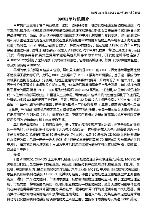
英文翻译系别专业班级学生姓名学号指导教师Introduction and application of AT89C51 Microcontrollers are used in a multitude of commercial applications such as modems, motor-control systems, air conditioner control systems, automotive engine and among others. The high processing speed and enhanced peripheral set of these microcontrollers make them suitable for such high-speed event-based applications. However, these critical application domains also require that these microcontrollers are highly reliable. The high reliability and low market risks can be ensured by a robust testing process and a proper tools environment for the validation of these microcontrollers both at the component and at the system level. Intel Plaform Engineering department developed an object-oriented multi-threaded test environment for the validation of its AT89C51 automotive microcontrollers. The goals of this environment was not only to provide a robust testing environment for the AT89C51 automotive microcontrollers, but to develop an environment which can be easily extended and reused for the validation of several other future microcontrollers. The environment was developed in conjunction with Microsoft Foundation Classes (AT89C51).The paper describes the design and mechanism of this test environment, its interactions with various hardware/software environmental components, and how to use AT89C51.1. IntroductionThe 8-bit AT89C51 CHMOS microcontrollers are designed to handle high-speed calculations and fast input/output operations. MCS 51 microcontrollers are typically used for high-speed event control systems. Commercial applications include modems, motor-control systems, printers, photocopiers, air conditioner control systems, disk drives, and medical instruments. The automotive industry use MCS 51 microcontrollers in engine-control systems, airbags, suspension systems, and antilock braking systems (ABS).The AT89C51 is especially well suited to applications that benefit from its processing speed and enhanced on-chip peripheral functions set, such as automotive power-train control, vehicle dynamic suspension, antilock braking, and stability control applications. Because of these critical applications, the market requires a reliable cost-effective controller with a low interrupt latency response, ability to service the high number of time and event driven integrated peripherals needed in real time applications, and a CPU with above average processing power in a single package. The financial and legal risk of having devices that operate unpredictably is very high. Once in the market, particularly in mission critical applications such as anautopilot or anti-lock braking system, mistakes are financially prohibitive. Redesign costs can run as high as a $500K, much more if the fix means back annotating it across a product family that share the same core and/or peripheral design flaw. In addition, field replacements of components is extremely expensive, as the devices are typically sealed in modules with a total value several times that of the component. To mitigate these problems, it is essential that comprehensive testing of the controllers be carried out at both the component level and system level under worst case environmental and voltage conditions.This complete and thorough validation necessitatesnot only a well-defined process but also a proper environment and tools to facilitate and execute the mission successfully.Intel Chandler Platform Engineering group provides postsilicon system validation (SV) of various micro-controllers and processors. The system validation process can be broken into three major parts.The type of the device and its application requirements determine which types of testing are performed on the device.The AT89C51 provides the following standard features: 4Kbytes of Flash, 128 bytes of RAM, 32 I/O lines, two 16-bittimer/counters, a five vector two-level interrupt architecture,a full duple ser -ial port, on-chip oscillator and clock circuitry.In addition, the AT89C51 is designed with static logic for operation down to zero frequency and supports two software selectable power saving modes. The Idle Mode stops the CPU while allowing the RAM, timer/counters,serial port and interrupt sys -tem to continue functioning. The Power-down Mode saves the RAM contents but freezes the oscil -lator disabling all other chip functions until the next hardware reset.Pin Configurations Block Diagram2 Pin DescriptionVCC Supply voltage.GND Ground.Port 0Port 0 is an 8-bit open-drain bi-directional I/O port. As an output port, each pin can sink eight TTL inputs. When 1s are written to port 0 pins, the pins can be used as high impedance inputs.Port 0 may also be configured to be the multiplexed low order address/data bus during accesses to external program and data memory. In this mode P0 has internal pullups.Port 0 also receives the code bytes during Flash programming, and outputs the code bytes during program verification. External pullups are required during program verification.Port 1Port 1 is an 8-bit bi-directional I/O port with internal pullups.The Port 1 output buffers can sink/so -urce four TTL inputs.When 1s are written to Port 1 pins they are pulled high by the internal pullups and can be used as inputs. As inputs, Port1 pins that are externally being pulled low will source current (IIL) because ofthe internal pullups.Port 1 also receives the low-order address bytes during Flash programming and verification.Port 2Port 2 is an 8-bit bi-directional I/O port with internal pullups.The Port 2 output buffers can sink/source four TTL inputs.When 1s are written to Port 2 pins they are pulled high by the internal pullups and can be used as inputs. As inputs, Port 2 pins that are externally being pulled low will source current (IIL) because of the internal pullups.Port 2 emits the high-order address byte during fetches from external program memory and during accesses to Port 2 pins that are externally being pulled low will source current (IIL) because of the internal pullups.Port 2 emits the high-order address byte during fetches from external program memory and during accesses to external data memory that use 16-bit addresses (MOVX @DPTR). In this application, it uses strong internal pull-ups when emitting 1s.During accesses to external data memory that use 8-bit addresses (MOVX @ RI), Port 2 emitsthe contents of the P2 Special Function Register.Port 2 also receives the high-order address bits and some control signals durin Flash programming and verification.Port 3Port 3 is an 8-bit bi-directional I/O port with internal pullups.The Port 3 output buffers can sink/sou -rce four TTL inputs.When 1s are written to Port 3 pins they are pulled high by the internal pullups and can be used as inputs. As inputs,Port 3 pins that are externally being pulled low will source current (IIL) because of the pullups. Port 3 also serves the functions of various special featuresof the AT89C51 as listed below:3 Port Pin Alternate FunctionsP3.0 RXD(serial input port)P3.1 TXD (serial output port)P3.2 INT0 (external interrupt 0)P3.3 INT1 (external interrupt 1)P3.4 T0 (timer 0 external input)P3.5 T1 (timer 1 external input)P3.6 WR (external data memory write strobe)P3.7 RD (external data memory read strobe)Port 3 also receives some control signals for Flash programming and verification. RSTReset input. A high on this pin for two machine cycles while the oscillator is running resets the device.ALE/PROGAddress Latch Enable output pulse for latching the low byte of the address during accesses to external memory. This pin is also the program pulse input (PROG)during Flash programming.In normal operation ALE is emitted at a constant rate of 1/6 the oscillator frequency, and may be used for external timing or clocking purposes. Note, however, that one ALE pulse is skipped duri -ng each access to external DataMemory.If desired, ALE operation can be disabled by setting bit 0 of SFR location 8EH. With the bit set, ALE is active only during a MOVX or MOVC instruction. Otherwise, the pin is weakly pulled high. Setting the ALE-disable bit has no effect if the microcontroller is in external execution mode.PSENProgram Store Enable is the read strobe to external program memory. When the AT89C51 is executing code from external program memory, PSEN is activated twice each machine cycle, except that two PSEN activations are skipped during each access to external data memory.EA/VPPExternal Access Enable. EA must be strapped to GND in order to enable the device to fetch code from external program memory locations starting at 0000H up to FFFFH. Note, however, that if lock bit 1 is programmed, EA will be internally latched on reset.EA should be strapped to VCC for internal program executions. This pin also receives the 12-volt programming enable voltage (VPP) during Flash programming, for parts that require 12-volt VPP.XTAL1Input to the inverting oscillator amplifier and input to the internal clock operating circuit.XTAL2Output from the inverting oscillator amplifier.4 Oscillator CharacteristicsXTAL1 and XTAL2 are the input and output, respectively, of an inverting amplifier which can be configured for use as an on-chip oscillator, as shown in Figure 1. Either a quartz crystal or ceramic resonator may be used. To drive the device from an external clock source, XTAL2 should be left unconnected while XTAL1 is driven as shown in Figure 2.There are no requirements on the duty cycle of the external clock signal, since the input to the internal clocking circuitry is through a divide-by-two flip-flop, but minimum and maximum voltage high and low time specifications must be observed.Idle ModeIn idle mode, the CPU puts itself to sleep while all the onchip peripherals remain active. The mode is invoked by software. The content of the on-chip RAM and all the special functions registers remain unchanged during this mode. The idle mode can be terminated by any enabled interrupt or by a hardware reset. It should be noted that when idle is terminated by a hard ware reset, the device normally resumes program execution, from where it left off, up to two machine cycles before the internal reset algorithm takes control. On-chip hardware inhibits access to internal RAM in this event, but access to the port pins is not inhibited. To eliminate the possibility of an unexpected write to a port pin when Idle is terminated by reset, theinstruction following the one that invokes Idle should not be one that writes to a port pin or to external memory.Figure 1. Oscillator Connections Figure 2. External Clock Drive Configuration Note: C1, C2 = 30 pF . .10 pF for Crystals = 40 pF . .10 pF for Ceramic Resonators In the power-down mode, the oscillator is stopped, and the instruction that invokes.5 Power-down Modepower-down is the last instruction executed. The on-chip RAM and Special Function Registers retain their values until the power-down mode is terminated. The only exit from power-down is a hardware reset. Reset redefines the SFRs but does not change the on-chip RAM. The reset should not be activated before VCC is restored to its normal operating level and must be held active long enough to allow the oscillator to restart and stabilize.Status of External Pins During Idle and Power-down Modes Mode Program Memory ALE PSEN PORT0 PORT1 PORT2 PORT3Idle Internal 1 1 Data Data Data DataIdle External 1 1 Float Data Address DataPower-down Internal 0 0 Data Data Data DataPower-down External 0 0 Float Data Data DataProgram Memory Lock BitsOn the chip are three lock bits which can be left unprogrammed (U) or can be programmed (P) to obtain the additional features listed in the table below.Lock Bit Protection Modes Program Lock Bits Protection Type LB1 LB2 LB31 U U U No program lock features2 P U U MOVC instructions executed from external program memory are disabled from etching code bytes from internal memory.3 P P U Same as mode 2, also verify is disabled4 P P P Same as mode 3, also external execution is disabledWhen lock bit 1 is programmed, the logic level at the EA pin is sampled and latched during reset. If the device is powered up without a reset, the latch initializes to a random value, and holds that value until reset is activated. It is necessary that the latched value of EA be in agreement with the current logic level at that pin in order for the device to function properly.6 Programming the FlashThe AT89C51 is normally shipped with the on-chip Flash memory array in the erased state (that is, contents = FFH) and ready to be programmed. The programming interface accepts either a high-voltage (12-volt) or a low-voltage (VCC) program enable signal. The low-voltage programming mode provides a convenient way to program the AT89C51 inside the user’s system, while the high-voltage programming mode is compatible with conventional thirdparty Flash or EPROM programmers. The AT89C51 is shipped with either the high-voltage or low-voltage programming mode enabled. The respective top-side marking and device signature codes are listed in the following table.VPP = 12V VPP = 5VTop-Side Mark AT89C51 AT89C51xxxx xxxx-5yyww yywwSignature (030H) = 1EH (030H) = 1EH(031H) = 51H (031H) = 51H(032H) =F FH (032H) = 05HThe AT89C51 code memory array is programmed byte-bybyte in either programming mode. To program any nonblank byte in the on-chip Flash Memory, the entire memory must be erased using the Chip Erase Mode.7 Programming AlgorithmBefore programming the AT89C51, the address, data and control signals should be set up according to the Flash programming mode table and Figure 3 and Figure 4. To program the AT89C51, take the following steps.1. Input the desired memory location on the address lines.2. Input the appropriate data byte on the data lines.3. Activate the correct combination of control signals.4. Raise EA/VPP to 12V for the high-voltage programming mode.5. Pulse ALE/PROG once to program a byte in the Flash array or the lock bits. The byte-write cycle is self-timed and typically takes no more than 1.5 ms. Repeat steps 1 through 5, changing the address and data for the entire array or until the end of the object file is reached.Data Polling:The AT89C51 features Data Polling to indicate the end of a write cycle. During a write cycle, an attempted read of the last byte written will result in the complement of the written datum on PO.7. Once the write cycle has been completed, true data are valid on all outputs, and the next cycle may begin. Data Polling may begin any time after a write cycle has been initiated.Ready/Busy:The progress of byte programming can also be monitored by the RDY/BSY output signal. P3.4 is pulled low after ALE goes high during programming to indicate BUSY. P3.4 is pulled high again when programming is done to indicateREADY.Program Verify: If lock bits LB1 and LB2 have not been programmed, the programmed code data can be read back via the address and data lines for verification.The lock bits cannot be verified directly. Verification of the lock bits is achieved by observing that their features are enabled.8 Flash Programming ModesMode RST PSEN ALE/PROG EA/VPP P2.6 P2.7 P3.6 P3.7Write Code Data H L H/12V L H H HRead Code Data H L H H L L H HWriteLockBit -1 H L H/12V H H H HBit -2 H L H/12V H H L LBit -3 H L H/12V H L L LChip Erase H LH/12V H L L LRead Signature Byte H L H H L L L LNote: 1. Chip Erase requires a 10 ms PROG pulse.Figure 3. Programming the Flash Figure 4. Verifying the FlashFlash Programming and Verification Waveforms -High-voltage Mode (VPP = 12V) Flash Programming and Verification Waveforms -Low-voltage Mode (VPP = 5V)9 Chip EraseThe entire Flash array is erased electrically by using the proper combination of control signals and by holding ALE/PROG low for 10 ms. The code array is written with all “1”s. The chip erase operation must be executed befor e the code memory can be re-programmed.Reading the Signature Bytes:The signature bytes are read by the same procedure as a normal verification of locations 030H, 031H, and 032H, except that P3.6 and P3.7 must be pulled to a logic low. The values returned areas follows.(030H) = 1EH indicates manufactured by Atmel(031H) = 51H indicates 89C51(032H) = FFH indicates 12V programming(032H) = 05H indicates 5V programmingProgramming InterfaceEvery code byte in the Flash array can be written and the entire array can be erased by using the appropriate combination of control signals. The write operation cycle is selftimed and once initiated, will automatically time itself to completion. Flash Programming and Verification Characteristics TA = 0°C to 70°C, VCC = 5.0 . .10%10 Symbol Parameter Min Max UnitsVPP(1) Programming EnableV oltage11.5 12.5 VIPP(1) Programming Enable Current 1.0 mA1/tCLCL Oscillator Frequency 3 24 MHztA VGL Address Setup to PROGLow48tCLCLtGHAX Address Hold After PROG 48tCLCLtDVGL Data Setup to PROG Low 48tCLCLtGHDX Data Hold After PROG 48tCLCLtEHSH P2.7(ENABLE) High to VPP 48tCLCLtSHGL VPP Setup to PROG Low 10 μstGHSL(1) VPP Hold After PROG 10 μstGLGH PROG Width 1 110 μstA VQV Address to Data Valid 48tCLCLtELQV ENABLE Low to Data Valid 48tCLCLtEHQZ Data Float After ENABLE 0 48tCLCLtGHBL PROG High to BUSY Low 1.0 μstWC Byte Write Cycle Time 2.0 msNote: 1. Only used in 12-volt programming mode.Absolute Maximum Ratings*Operating Temperature......................... -55°C to +125°CStorage Temperature ............................. -65°C to +150°CV oltage on Any Pin with Respect to Ground ............-1.0V to +7.0VMaximum Operating V oltage .................................. 6.6VDC Output Current....................................... 15.0 mA11 DC CharacteristicsTA = -40°C to 85°C, VCC = 5.0V . .20% (unless otherwise noted)Symbol Parameter Condition Min Max Units VIL Input Low-voltage (Except EA) -0.5 0.2 VCC 0.1 -VVIL1 nput Low-voltage (EA) -0.5 0.2 VCC 0.3 -VVIH iput High-voltage (Except XTAL1, RST) 0.2 VCC +0.9 VCC + 0.5 VVIH1 Input High-voltage (XTAL1, RST) 0.7 VCC VCC + 0.5 VVOL Output Low-voltage(1) (Ports 1,2,3) IOL = 1.6 mA 0.45 VVOL1 Output Low-voltage(1) (Port 0, ALE, PSEN) IOL = 3.2 mA 0.45 VVOH Output High-voltage (Ports 1,2,3, ALE, PSEN) IOH = -60 μA, VCC = 5V . .10% 2.4 VIOH = -25 μA 0.75 VCC VIOH = -10 μA 0.9 VCC VVOH1 Output High-voltage (Port 0 in External Bus Mode) IOH = -800 μA, VCC = 5V . .10% 2.4 VIOH = -300μA, 0.75 VCC VIOH = -80μA, 0.9 VCC VIIL Logical 0 Input Current (Ports 1,2,3)VIN = 0.45V -50 μ AITL Logical 1 to 0 Transition Current (Ports 1,2,3) VIN = 2V, VCC = 5V . .10% -650 μ AILI Input Leakage Current (Port 0, EA) 0.45 < VIN < VCC . 10 μ A RRST Reset Pull-down Resistor 50 300 K.CIO Pin Capacitance Test Freq. = 1 MHz, TA = 25°C 10 pFICC Power Supply Current Active Mode, 12 MHz 20 mA Idle Mode, 12 MHz 5 mA Power-down Mode(2) VCC = 6V 100 μ A VCC = 3V 40 μ A12 AC CharacteristicsUnder operating conditions, load capacitance for Port 0, ALE/PROG, and PSEN = 100 pF; load capacitance for all other outputs = 80 pF.External Program and Data Memory Characteristics Symbol ParameterFrequency 12 MHz Oscillator 16 to 24 MHz Oscillator Units Min Max Min Max 1/tCLCL Oscillator 0 24 MHztLHLL ALE Pulse Width 127 2tCLCL-40 40 ns nstA VLL Address Valid to ALE Low 43 tCLCL-13 nstLLAX Address Hold After ALE Low 48 tCLCL-20 nstLLIV ALE Low to Valid Instruction In 233 4tCLCL-65 nstLLPL ALE Low to PSEN Low 43 tCLCL-13 nstPLPH PSEN Pulse Width 205 3tCLCL-20 nstPLIV PSEN Low to Valid Instruction In 145 3tCLCL-45 nstPXIX Input Instruction Hold After PSEN 0 0 nstPXIZ Input Instruction Float After PSEN 59 tCLCL-10 nstPXA V PSEN to Address Valid 75 tCLCL-8 nstA VIV Address to Valid Instruction In 312 5tCLCL-55 nstPLAZ PSEN Low to Address Float 10 10 nstRLRH RD Pulse Width 400 6tCLCL-100 nstWLWH WR Pulse Width 400 6tCLCL-100 nstRLDV RD Low to Valid Data In 252 5tCLCL-90 nstRHDX Data Hold After RD 0 0 ns 13tRHDZ Data Float After RD 97 2tCLCL-28 nstLLDV ALE Low to Valid Data In 517 8tCLCL-150 nstA VDV Address to Valid Data In 585 9tCLCL-165 nstLLWL ALE Low to RD or WR Low 200 300 3tCLCL-50 3tCLCL+50 nstA VWL Address to RD or WR Low 203 4tCLCL-75 nstQVWX Data Valid to WR Transition 23 tCLCL-20 nstQVWH Data Valid to WR High 433 7tCLCL-120 nstWHQX Data Hold After WR 33 tCLCL-20 nstRLAZ RD Low to Address Float 0 0 nstWHLH RD or WR High to ALE High 43 123 tCLCL-20 nsExternal Program Memory Read CycleExternal Data Memory Read CycleExternal Data Memory Write Cycle External Data Memory Write CycleExternal Clock Drive WaveformsExternal Clock DriveSymbol Parameter Min Max Units1/tCLCL Oscillator Frequency 0 24 MHztCLCL Clock Period 41.6 nstCHCX High Time 15 nstCLCX Low Time 15 nstCLCH Rise Time 20 nstCHCL Fall Time ns 20 nsSerial Port Timing:Shift Register Mode Test Conditions(VCC = 5.0 V . .20%; Load Capacitance = 80 pF)Symbol Parameter 12 MHz Osc Variable Oscillator Units UnitsMin Max Min MaxtXLXL Serial Port Clock Cycle Time 1.0 12tCLCL μstQVXH Output Data Setup to Clock Rising Edge 700 10tCLCL-133 nstXHQX Output Data Hold After Clock Rising Edge 50 2tCLCL-117 nstXHDX Input Data Hold After Clock Rising Edge 0 0 nstXHDV Clock Rising Edge to Input Data Valid 700 10tCLCL-133 ns 13 ShiftRegister Mode Timing Waveforms AC Testing Input/Output Waveforms Float WaveformsA microcomputer interface converts information between two forms. Outside the microcomputer the information handled by an electronic system exists as a physical signal, but within the program, it is represented numerically. The function of any interface can be broken down into a number of operations which modify the data in some way, so that the process of conversion between the external and internal forms is carried out in a number of steps.An analog-to-digital converter(ADC) is used to convert a continuously variable signal to a corresponding digital form which can take any one of a fixed number of possible binary values. If the output of the transducer does not vary continuously, no ADC is necessary. In this case the signal conditioning section must convert the incoming signal to a form which can be connected directly to the next part of the interface, the input/output section of the microcomputer itself.Output interfaces take a similar form, the obvious difference being that here the flow of information is in the opposite direction; it is passed from the program to the outside world. In this case the program may call an output subroutine which supervises the operation of the interface and performs the scaling numbers which may be needed for a digital-to-analog converter(DAC). This subroutine passes information in turn to an output device which produces a corresponding electrical signal, which could be converted into analog form using a DAC. Finally the signal is conditioned(usually amplified) to a form suitable for operating an actuator.The signals used within microcomputer circuits are almost always too small to be connected directly to the “outside world” and some kind of interface must be used to translate them to a more appropriate form. The design of section of interface circuits is one of the most important tasks facing the engineer wishing to apply microcomputers. We have seen that in microcomputers information is represented as discrete patterns of bits; this digital form is most useful when the microcomputer is to be connected to equipment which can only be switched on or off, where each bit might represent the state of a switch or actuator.To solve real-world problems, a microcontroller must have more than just a CPU, a program, and a data memory. In addition, it must contain hardware allowing the CPU to access information from the outside world. Once the CPU gathers information and processes the data, it must also be able to effect change on some portion of the outside world.These hardware devices, called peripherals, are the CPU’s window to theoutside. The most basic form of peripheral available on microcontrollers is the general purpose I70 port. Each of the I/O pins can be used as either an input or an output. The function of each pin is determined by setting or clearing corresponding bits in a corresponding data direction register during the initialization stage of a program. Each output pin may be driven to either a logic one or a logic zero by using CPU instructions to pin may be viewed (or read.) by the CPU using program instructions.Some type of serial unit is included on microcontrollers to allow the CPU to communicate bit-serially with external devices. Using a bit serial format instead of bit-parallel format requires fewer I/O pins to perform the communication function, which makes it less expensive, but slower. Serial transmissions are performed either synchronously or asynchronously.AT89C51的介绍及运用单片机广泛应用于商业:诸如调制解调器,电动机控制系统,空调控制系统,汽车发动机和其他一些领域。
89c51计数器汇编语言
89c51是一种8位单片机,具有有限的指令集。
以下是一个简单的89c51计数器的汇编语言程序示例:
```
ORG 0H ;程序起始地址
mov R0,#00H ;将R0寄存器置零
mov R1,#01H ;将R1寄存器置一
LOOP: ;循环开始
inc R0 ;递增R0寄存器的值
;这里可以添加其他要执行的指令
cjne R0,#10H,LOOP ;比较R0寄存器的值和十进制数10,如果不相等则跳转到LOOP标签处,继续执行循环
END ;程序结束
```
这个程序将使用R0寄存器作为计数器,并在R0寄存器的值递增到十进制数10时停止循环。
在循环内部,您可以添加其他要执行的指令来实现更复杂的功能。
关于单片机at89c51的外文翻译5000字英文篇一:毕业设计外文翻译单片机AT89C51附件1:外文资料翻译译文AT89C51主要性能参数:与MCS-51产品如前所述完全兼容4K字节可重檫写Flash闪速存储器1000次檫写周期全静态操作:0HZ-24MHZ三级加密程序存储器128*8字节内部RAM32个可编程I/O口线2个16位定时/记数器6个中断源可编程串行UART通道低功耗空闲和掉电操作方式功能特性概述:AT89C51提供更多以下标准功能:4K字节Flash闪速存储器,128字节内部RAM,32个I/O口线,两个16位定时/记数器,一个5向量两级中断结构,一个全双工串行通信口,片内振荡器妥善钟电路。
同时,AT89C51可降至0HZ的静态逻辑操作,并支持两种软件可选的节电工作模式。
空闲方式停止CPU的工作,但允许RAM,定时/记数器,串行通信口及中断系统继续工作。
掉电方式保存RAM中的内容,但振荡器停止工作直到下一个硬件逊位。
AT89C51是美国ATMEL公司生产的低电压,高性能CMOS8位单片机,片内含4k bytes的可反复擦写的只读程序存储器(PEROM)和128 bytes的随机存取数据存储器(RAM),器件采用ATMEL公司的高密度、非易失性存储技术生产,兼容标准MCS-51指令系统,片内置通用8位中央处理器(CPU)和Flash存储单元,功能强大AT89C51单片机用法可为您提供许多高性价比的应用场合,可灵活科技领域应用于各种支配领域。
AT89C51方框图引脚功能说明·Vcc:电源电压·GND:地·P0 口:P0 口是一组8 位漏极开路型双向I/O 口,也即地址/数据总线复用口。
作为输出口用时,每位能吸收电流的方式驱动8个TTL逻辑门电路,对端口写“1”可作为差阻抗输入端用。
在访问外部数据存储器或程序存储器时,这组口线分时转换地址(低8位)和数据总线复用,在访问期间激活内部上拉电阻。
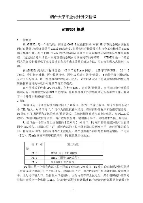
89C51单片机中文资料AT89C51是一种带4K字节闪烁可编程可擦除只读存储器(FPEROM—Falsh Programmable and Erasable Read Only Memory)的低电压,高性能CMOS8位微处理器,俗称单片机。
该器件采用ATMEL高密度非易失存储器制造技术制造,与工业标准的MCS-51指令集和输出管脚相兼容。
由于将多功能8位CPU和闪烁存储器组合在单个芯片中,ATMEL的AT89C51是一种高效微控制器,为很多嵌入式控制系统提供了一种灵活性高且价廉的方案。
1.主要特性:·与MCS-51 兼容·4K字节可编程闪烁存储器寿命:1000写/擦循环数据保留时间:10年·全静态工作:0Hz-24Hz ·三级程序存储器锁定·128*8位内部RAM·32可编程I/O线·两个16位定时器/计数器·5个中断源·可编程串行通道·低功耗的闲置和掉电模式·片内振荡器和时钟电路2.管脚说明:VCC:供电电压。
GND:接地。
P0口:P0口为一个8位漏级开路双向I/O口,每脚可吸收8TTL 门电流。
当P1口的管脚第一次写1时,被定义为高阻输入。
P0能够用于外部程序数据存储器,它可以被定义为数据/地址的第八位。
在FIASH 编程时,P0 口作为原码输入口,当FIASH进行校验时,P0输出原码,此时P0外部必须被拉高。
P1口:P1口是一个内部提供上拉电阻的8位双向I/O口,P1口缓冲器能接收输出4TTL门电流。
P1口管脚写入1后,被内部上拉为高,可用作输入,P1口被外部下拉为低电平时,将输出电流,这是由于内部上拉的缘故。
在FLASH编程和校验时,P1口作为第八位地址接收。
P2口:P2口为一个内部上拉电阻的8位双向I/O口,P2口缓冲器可接收,输出4个TTL门电流,当P2口被写“1”时,其管脚被内部上拉电阻拉高,且作为输入。
AT89S51概述1 一般概述该AT89S51是一个低功耗,高性能CMOS 8位微控制器,可在4K字节的系统内编程的闪存存储器。
该设备是采用Atmel的高密度、非易失性存储器技术和符合工业标准的80C51指令集和引脚。
芯片上的Flash程序存储器在系统中可重新编程或常规非易失性内存编程。
通过结合通用8位中央处理器的系统内可编程闪存的单芯片, AT89S51是一个功能强大的微控制器提供了高度灵活的和具有成本效益的解决办法,可在许多嵌入式控制中应用。
在AT89S51提供以下标准功能: 4K字节的Flash闪存, 128字节的RAM , 32个 I / O线,看门狗定时器,两个数据指针,两个16位定时器/计数器, 5向量两级中断结构,全双工串行端口,片上振荡器和时钟电路。
此外, AT89S51设计了可降至零频率的静态逻辑操作和支持两种软件可选的节电工作模式。
在空闲模式下停止CPU的工作,但允许RAM 、定时器/计数器、串行接口和中断系统继续运行。
掉电模式保存RAM中的内容,停止振荡器工作并禁止其它所有部件工作,直到下一个外部中断或硬件复位。
2 端口P0端口是一个8位漏极开路双向I / O端口。
作为一个输出端口,每个引脚可驱动8个TTL输入。
对端口写“1”可作为高阻抗输入端用。
在访问外部程序和数据存储器时,P0端口也可以配置为复低阶地址/数据总线。
在访问期间激活内部上拉电阻。
在Flash编程时,PO端口接收指令字节,而在程序校验时,输出指令字节,同时要求外接上拉电阻。
P1端口是一个带内部上拉电阻的8位双向I /O端口。
P1端口的输出缓冲级可以驱动四个TTL输入。
对端口写“1”,通过内部的上拉电阻把端口拉到高电平,此时可作为输入口。
作为输入口时,因为内部存在上拉电阻,某个引脚被外部信号拉低时会输出一个电流(IIL),Flash编程和程序校验期间,P1接收低8位地址。
P2端口是一个带有内部上拉电阻的8位双向I/O端口。

AT89C51芯片介绍完整中英文翻译AT89C51 是一款由美国Atmel公司生产的低功耗、高性能的CMOS 8位微控制器。
AT89C51 是 8051 型系列的一员,采用汇编指令集,并具有大容量闪存。
该芯片具有广泛的应用范围,例如家居电器、工业控制、电子设备和通信设备等。
1.高速运算能力:AT89C51具有12兆赫兹的工作频率,可以实现高效率的数据处理和快速的响应速度。
2.强大的闪存容量:AT89C51的内存结构分为数据存储器和程序存储器两部分。
其中,数据存储器包括256字节的RAM和128字节的RAM。
程序存储器可以存储64KB的程序代码,为用户提供了大量的存储空间。
3.多种输入/输出功能:AT89C51具有4个输入/输出端口,每个端口拥有8个引脚,可用于和各种外设的连接,例如按键、LED灯和LCD显示屏等。
4.低功耗设计:AT89C51芯片采用CMOS技术,功耗低,有利于延长电池寿命并提高设备的节能性能。
5.多种通信接口:AT89C51集成了多种通信接口,例如串行口、并行口和SPI接口,支持与其他设备进行数据交互和通信。
AT89C51的工作原理是通过提供时钟信号来控制指令的执行流程。
该芯片的内部结构包括ALU(算术逻辑单元)、寄存器和时钟电路。
时钟信号通过振荡器提供,并通过时钟分频器来调整执行速度。
AT89C51可以执行各种算术和逻辑操作,包括加、减、乘、除、移位和逻辑运算等。
此外,它还具有中断功能,可以在设备发生特定事件时提供及时响应。
在软件开发方面,AT89C51芯片可使用C语言编程,并可使用汇编语言编写优化的指令。
Atmel公司还提供了一些强大的开发工具和集成开发环境(IDE),以帮助程序员开发和调试应用程序。
总结来说,AT89C51是一款功能强大、易于开发的微控制器芯片。
它具有高速运算能力、大容量闪存、多种通信接口和低功耗等优点,适用于多种领域的应用需求。
同时,AT89C51还提供了丰富的软件开发工具和开发环境,方便开发人员进行编程和调试。
89C51单片机简介单片机广泛应用于各个商业领域,比如:调制解调器,电动机控制系统,空调控制系统,汽车发动机和其他一些领域.这些单片机的高速处理速度和增强型外围设备集合使得它们适合于这种高速事件应用场合。
然而,这些关键应用领域对这些单片机有高度可靠的要求。
健壮的测试环境和用于验证这些无论在元部件层次还是系统级别的单片机的合适的工具环境保证了高可靠性和低市场风险。
Intel 平台工程部门开发了一种面向对象的用于验证它的AT89C51汽车单片机多线性测试环境。
这种环境的目标不仅是为AT89C51汽车单片机提供一种健壮测试环境,而且开发一种能够容易扩展并重复用来验证其他几种将来的单片机。
开发的这种环境连接了AT89C51.本文讨论了这种测试环境的设计和原理,它的和各种硬件、软件环境部件的交互性,以及如何使用AT89C51.早期的单片机都是8位或4位的。
其中最成功的是INTEL的8031,因为简单可靠而性能不错获得了很大的好评。
此后在8031上发展出了MCS51系列单片机系统。
基于这一系统的单片机系统直到现在还在广泛使用。
随着工业控制领域要求的提高,开始出现了16位单片机,但因为性价比不理想并未得到很广泛的应用。
90年代后随着消费电子产品大发展,单片机技术得到了巨大的提高.随着INTEL i960系列特别是后来的ARM系列的广泛应用,32位单片机迅速取代16位单片机的高端地位,并且进入主流市场。
而传统的8位单片机的性能也得到了飞速提高,处理能力比起80年代提高了数百倍。
目前,高端的32位单片机主频已经超过300MHz,性能直追90年代中期的专用处理器,而普通的型号出厂价格跌落至1美元,最高端的型号也只有10美元。
当代单片机系统已经不再只在裸机环境下开发和使用,大量专用的嵌入式操作系统被广泛应用在全系列的单片机上。
而在作为掌上电脑和手机核心处理的高端单片机甚至可以直接使用专用的Windows和Linux操作系统。

89c51计数器汇编语言89C51是一种常用的单片机,它采用汇编语言进行编程。
在89C51中,计数器是一种非常重要的功能,它可以用来实现各种计数任务。
本文将介绍89C51计数器的使用方法和一些常见的应用场景。
首先,我们需要了解89C51中计数器的基本原理。
89C51有两个8位计数器,分别是T0和T1。
这两个计数器可以通过特定的寄存器进行配置和控制。
在89C51中,计数器可以工作在两种模式下:定时器模式和计数器模式。
在定时器模式下,计数器可以根据设定的时间间隔自动进行计数。
我们可以通过设置相关的寄存器来控制计数器的工作频率和计数范围。
例如,我们可以将T0计数器设置为10ms,并且设置计数范围为0-255。
这样,每隔10ms,T0计数器就会自动加1,当计数器达到255时,会产生一个中断信号。
在计数器模式下,计数器可以根据外部输入信号进行计数。
我们可以将外部信号连接到T0或T1引脚上,当信号发生变化时,计数器就会自动加1或减1。
这种模式下,计数器可以用来实现各种计数任务,例如计算脉冲数量、测量时间间隔等。
接下来,我们将介绍一些常见的89C51计数器的应用场景。
首先是脉冲计数。
我们可以将外部脉冲信号连接到T0或T1引脚上,通过计数器来统计脉冲的数量。
例如,我们可以将T0设置为计数模式,当外部信号发生一个脉冲时,T0计数器就会加1。
通过读取计数器的值,我们就可以知道脉冲的数量。
其次是测量时间间隔。
我们可以使用定时器模式来测量两个事件之间的时间间隔。
例如,我们可以将T1设置为定时器模式,每隔一段时间产生一个中断信号。
当第一个事件发生时,我们可以启动T1计数器,当第二个事件发生时,我们可以停止T1计数器。
通过读取计数器的值,我们就可以得到两个事件之间的时间间隔。
最后是频率测量。
我们可以使用计数器模式来测量外部信号的频率。
例如,我们可以将外部信号连接到T0引脚上,当信号发生一个周期时,T0计数器就会加1。
通过读取计数器的值,我们就可以得到外部信号的频率。
英文翻译系别专业班级学生姓名学号指导教师Introduction and application of AT89C51 Microcontrollers are used in a multitude of commercial applications such as modems, motor-control systems, air conditioner control systems, automotive engine and among others. The high processing speed and enhanced peripheral set of these microcontrollers make them suitable for such high-speed event-based applications. However, these critical application domains also require that these microcontrollers are highly reliable. The high reliability and low market risks can be ensured by a robust testing process and a proper tools environment for the validation of these microcontrollers both at the component and at the system level. Intel Plaform Engineering department developed an object-oriented multi-threaded test environment for the validation of its AT89C51 automotive microcontrollers. The goals of this environment was not only to provide a robust testing environment for the AT89C51 automotive microcontrollers, but to develop an environment which can be easily extended and reused for the validation of several other future microcontrollers. The environment was developed in conjunction with Microsoft Foundation Classes (AT89C51).The paper describes the design and mechanism of this test environment, its interactions with various hardware/software environmental components, and how to use AT89C51.1. IntroductionThe 8-bit AT89C51 CHMOS microcontrollers are designed to handle high-speed calculations and fast input/output operations. MCS 51 microcontrollers are typically used for high-speed event control systems. Commercial applications include modems, motor-control systems, printers, photocopiers, air conditioner control systems, disk drives, and medical instruments. The automotive industry use MCS 51 microcontrollers in engine-control systems, airbags, suspension systems, and antilock braking systems (ABS).The AT89C51 is especially well suited to applications that benefit from its processing speed and enhanced on-chip peripheral functions set, such as automotive power-train control, vehicle dynamic suspension, antilock braking, and stability control applications. Because of these critical applications, the market requires a reliable cost-effective controller with a low interrupt latency response, ability to service the high number of time and event driven integrated peripherals needed in real time applications, and a CPU with above average processing power in a single package. The financial and legal risk of having devices that operate unpredictably is very high. Once in the market, particularly in mission critical applications such as anautopilot or anti-lock braking system, mistakes are financially prohibitive. Redesign costs can run as high as a $500K, much more if the fix means back annotating it across a product family that share the same core and/or peripheral design flaw. In addition, field replacements of components is extremely expensive, as the devices are typically sealed in modules with a total value several times that of the component. To mitigate these problems, it is essential that comprehensive testing of the controllers be carried out at both the component level and system level under worst case environmental and voltage conditions.This complete and thorough validation necessitatesnot only a well-defined process but also a proper environment and tools to facilitate and execute the mission successfully.Intel Chandler Platform Engineering group provides postsilicon system validation (SV) of various micro-controllers and processors. The system validation process can be broken into three major parts.The type of the device and its application requirements determine which types of testing are performed on the device.The AT89C51 provides the following standard features: 4Kbytes of Flash, 128 bytes of RAM, 32 I/O lines, two 16-bittimer/counters, a five vector two-level interrupt architecture,a full duple ser -ial port, on-chip oscillator and clock circuitry.In addition, the AT89C51 is designed with static logic for operation down to zero frequency and supports two software selectable power saving modes. The Idle Mode stops the CPU while allowing the RAM, timer/counters,serial port and interrupt sys -tem to continue functioning. The Power-down Mode saves the RAM contents but freezes the oscil -lator disabling all other chip functions until the next hardware reset.Pin Configurations Block Diagram2 Pin DescriptionVCC Supply voltage.GND Ground.Port 0Port 0 is an 8-bit open-drain bi-directional I/O port. As an output port, each pin can sink eight TTL inputs. When 1s are written to port 0 pins, the pins can be used as high impedance inputs.Port 0 may also be configured to be the multiplexed low order address/data bus during accesses to external program and data memory. In this mode P0 has internal pullups.Port 0 also receives the code bytes during Flash programming, and outputs the code bytes during program verification. External pullups are required during program verification.Port 1Port 1 is an 8-bit bi-directional I/O port with internal pullups.The Port 1 output buffers can sink/so -urce four TTL inputs.When 1s are written to Port 1 pins they are pulled high by the internal pullups and can be used as inputs. As inputs, Port1 pins that are externally being pulled low will source current (IIL) because ofthe internal pullups.Port 1 also receives the low-order address bytes during Flash programming and verification.Port 2Port 2 is an 8-bit bi-directional I/O port with internal pullups.The Port 2 output buffers can sink/source four TTL inputs.When 1s are written to Port 2 pins they are pulled high by the internal pullups and can be used as inputs. As inputs, Port 2 pins that are externally being pulled low will source current (IIL) because of the internal pullups.Port 2 emits the high-order address byte during fetches from external program memory and during accesses to Port 2 pins that are externally being pulled low will source current (IIL) because of the internal pullups.Port 2 emits the high-order address byte during fetches from external program memory and during accesses to external data memory that use 16-bit addresses (MOVX @DPTR). In this application, it uses strong internal pull-ups when emitting 1s.During accesses to external data memory that use 8-bit addresses (MOVX @ RI), Port 2 emitsthe contents of the P2 Special Function Register.Port 2 also receives the high-order address bits and some control signals durin Flash programming and verification.Port 3Port 3 is an 8-bit bi-directional I/O port with internal pullups.The Port 3 output buffers can sink/sou -rce four TTL inputs.When 1s are written to Port 3 pins they are pulled high by the internal pullups and can be used as inputs. As inputs,Port 3 pins that are externally being pulled low will source current (IIL) because of the pullups. Port 3 also serves the functions of various special featuresof the AT89C51 as listed below:3 Port Pin Alternate FunctionsP3.0 RXD(serial input port)P3.1 TXD (serial output port)P3.2 INT0 (external interrupt 0)P3.3 INT1 (external interrupt 1)P3.4 T0 (timer 0 external input)P3.5 T1 (timer 1 external input)P3.6 WR (external data memory write strobe)P3.7 RD (external data memory read strobe)Port 3 also receives some control signals for Flash programming and verification. RSTReset input. A high on this pin for two machine cycles while the oscillator is running resets the device.ALE/PROGAddress Latch Enable output pulse for latching the low byte of the address during accesses to external memory. This pin is also the program pulse input (PROG)during Flash programming.In normal operation ALE is emitted at a constant rate of 1/6 the oscillator frequency, and may be used for external timing or clocking purposes. Note, however, that one ALE pulse is skipped duri -ng each access to external DataMemory.If desired, ALE operation can be disabled by setting bit 0 of SFR location 8EH. With the bit set, ALE is active only during a MOVX or MOVC instruction. Otherwise, the pin is weakly pulled high. Setting the ALE-disable bit has no effect if the microcontroller is in external execution mode.PSENProgram Store Enable is the read strobe to external program memory. When the AT89C51 is executing code from external program memory, PSEN is activated twice each machine cycle, except that two PSEN activations are skipped during each access to external data memory.EA/VPPExternal Access Enable. EA must be strapped to GND in order to enable the device to fetch code from external program memory locations starting at 0000H up to FFFFH. Note, however, that if lock bit 1 is programmed, EA will be internally latched on reset.EA should be strapped to VCC for internal program executions. This pin also receives the 12-volt programming enable voltage (VPP) during Flash programming, for parts that require 12-volt VPP.XTAL1Input to the inverting oscillator amplifier and input to the internal clock operating circuit.XTAL2Output from the inverting oscillator amplifier.4 Oscillator CharacteristicsXTAL1 and XTAL2 are the input and output, respectively, of an inverting amplifier which can be configured for use as an on-chip oscillator, as shown in Figure 1. Either a quartz crystal or ceramic resonator may be used. To drive the device from an external clock source, XTAL2 should be left unconnected while XTAL1 is driven as shown in Figure 2.There are no requirements on the duty cycle of the external clock signal, since the input to the internal clocking circuitry is through a divide-by-two flip-flop, but minimum and maximum voltage high and low time specifications must be observed.Idle ModeIn idle mode, the CPU puts itself to sleep while all the onchip peripherals remain active. The mode is invoked by software. The content of the on-chip RAM and all the special functions registers remain unchanged during this mode. The idle mode can be terminated by any enabled interrupt or by a hardware reset. It should be noted that when idle is terminated by a hard ware reset, the device normally resumes program execution, from where it left off, up to two machine cycles before the internal reset algorithm takes control. On-chip hardware inhibits access to internal RAM in this event, but access to the port pins is not inhibited. To eliminate the possibility of an unexpected write to a port pin when Idle is terminated by reset, theinstruction following the one that invokes Idle should not be one that writes to a port pin or to external memory.Figure 1. Oscillator Connections Figure 2. External Clock Drive Configuration Note: C1, C2 = 30 pF . .10 pF for Crystals = 40 pF . .10 pF for Ceramic Resonators In the power-down mode, the oscillator is stopped, and the instruction that invokes.5 Power-down Modepower-down is the last instruction executed. The on-chip RAM and Special Function Registers retain their values until the power-down mode is terminated. The only exit from power-down is a hardware reset. Reset redefines the SFRs but does not change the on-chip RAM. The reset should not be activated before VCC is restored to its normal operating level and must be held active long enough to allow the oscillator to restart and stabilize.Status of External Pins During Idle and Power-down Modes Mode Program Memory ALE PSEN PORT0 PORT1 PORT2 PORT3Idle Internal 1 1 Data Data Data DataIdle External 1 1 Float Data Address DataPower-down Internal 0 0 Data Data Data DataPower-down External 0 0 Float Data Data DataProgram Memory Lock BitsOn the chip are three lock bits which can be left unprogrammed (U) or can be programmed (P) to obtain the additional features listed in the table below.Lock Bit Protection Modes Program Lock Bits Protection Type LB1 LB2 LB31 U U U No program lock features2 P U U MOVC instructions executed from external program memory are disabled from etching code bytes from internal memory.3 P P U Same as mode 2, also verify is disabled4 P P P Same as mode 3, also external execution is disabledWhen lock bit 1 is programmed, the logic level at the EA pin is sampled and latched during reset. If the device is powered up without a reset, the latch initializes to a random value, and holds that value until reset is activated. It is necessary that the latched value of EA be in agreement with the current logic level at that pin in order for the device to function properly.6 Programming the FlashThe AT89C51 is normally shipped with the on-chip Flash memory array in the erased state (that is, contents = FFH) and ready to be programmed. The programming interface accepts either a high-voltage (12-volt) or a low-voltage (VCC) program enable signal. The low-voltage programming mode provides a convenient way to program the AT89C51 inside the user’s system, while the high-voltage programming mode is compatible with conventional thirdparty Flash or EPROM programmers. The AT89C51 is shipped with either the high-voltage or low-voltage programming mode enabled. The respective top-side marking and device signature codes are listed in the following table.VPP = 12V VPP = 5VTop-Side Mark AT89C51 AT89C51xxxx xxxx-5yyww yywwSignature (030H) = 1EH (030H) = 1EH(031H) = 51H (031H) = 51H(032H) =F FH (032H) = 05HThe AT89C51 code memory array is programmed byte-bybyte in either programming mode. To program any nonblank byte in the on-chip Flash Memory, the entire memory must be erased using the Chip Erase Mode.7 Programming AlgorithmBefore programming the AT89C51, the address, data and control signals should be set up according to the Flash programming mode table and Figure 3 and Figure 4. To program the AT89C51, take the following steps.1. Input the desired memory location on the address lines.2. Input the appropriate data byte on the data lines.3. Activate the correct combination of control signals.4. Raise EA/VPP to 12V for the high-voltage programming mode.5. Pulse ALE/PROG once to program a byte in the Flash array or the lock bits. The byte-write cycle is self-timed and typically takes no more than 1.5 ms. Repeat steps 1 through 5, changing the address and data for the entire array or until the end of the object file is reached.Data Polling:The AT89C51 features Data Polling to indicate the end of a write cycle. During a write cycle, an attempted read of the last byte written will result in the complement of the written datum on PO.7. Once the write cycle has been completed, true data are valid on all outputs, and the next cycle may begin. Data Polling may begin any time after a write cycle has been initiated.Ready/Busy:The progress of byte programming can also be monitored by the RDY/BSY output signal. P3.4 is pulled low after ALE goes high during programming to indicate BUSY. P3.4 is pulled high again when programming is done to indicateREADY.Program Verify: If lock bits LB1 and LB2 have not been programmed, the programmed code data can be read back via the address and data lines for verification.The lock bits cannot be verified directly. Verification of the lock bits is achieved by observing that their features are enabled.8 Flash Programming ModesMode RST PSEN ALE/PROG EA/VPP P2.6 P2.7 P3.6 P3.7Write Code Data H L H/12V L H H HRead Code Data H L H H L L H HWriteLockBit -1 H L H/12V H H H HBit -2 H L H/12V H H L LBit -3 H L H/12V H L L LChip Erase H LH/12V H L L LRead Signature Byte H L H H L L L LNote: 1. Chip Erase requires a 10 ms PROG pulse.Figure 3. Programming the Flash Figure 4. Verifying the FlashFlash Programming and Verification Waveforms -High-voltage Mode (VPP = 12V) Flash Programming and Verification Waveforms -Low-voltage Mode (VPP = 5V)9 Chip EraseThe entire Flash array is erased electrically by using the proper combination of control signals and by holding ALE/PROG low for 10 ms. The code array is written with all “1”s. The chip erase operation must be executed befor e the code memory can be re-programmed.Reading the Signature Bytes:The signature bytes are read by the same procedure as a normal verification of locations 030H, 031H, and 032H, except that P3.6 and P3.7 must be pulled to a logic low. The values returned areas follows.(030H) = 1EH indicates manufactured by Atmel(031H) = 51H indicates 89C51(032H) = FFH indicates 12V programming(032H) = 05H indicates 5V programmingProgramming InterfaceEvery code byte in the Flash array can be written and the entire array can be erased by using the appropriate combination of control signals. The write operation cycle is selftimed and once initiated, will automatically time itself to completion. Flash Programming and Verification Characteristics TA = 0°C to 70°C, VCC = 5.0 . .10%10 Symbol Parameter Min Max UnitsVPP(1) Programming EnableV oltage11.5 12.5 VIPP(1) Programming Enable Current 1.0 mA1/tCLCL Oscillator Frequency 3 24 MHztA VGL Address Setup to PROGLow48tCLCLtGHAX Address Hold After PROG 48tCLCLtDVGL Data Setup to PROG Low 48tCLCLtGHDX Data Hold After PROG 48tCLCLtEHSH P2.7(ENABLE) High to VPP 48tCLCLtSHGL VPP Setup to PROG Low 10 μstGHSL(1) VPP Hold After PROG 10 μstGLGH PROG Width 1 110 μstA VQV Address to Data Valid 48tCLCLtELQV ENABLE Low to Data Valid 48tCLCLtEHQZ Data Float After ENABLE 0 48tCLCLtGHBL PROG High to BUSY Low 1.0 μstWC Byte Write Cycle Time 2.0 msNote: 1. Only used in 12-volt programming mode.Absolute Maximum Ratings*Operating Temperature......................... -55°C to +125°CStorage Temperature ............................. -65°C to +150°CV oltage on Any Pin with Respect to Ground ............-1.0V to +7.0VMaximum Operating V oltage .................................. 6.6VDC Output Current....................................... 15.0 mA11 DC CharacteristicsTA = -40°C to 85°C, VCC = 5.0V . .20% (unless otherwise noted)Symbol Parameter Condition Min Max Units VIL Input Low-voltage (Except EA) -0.5 0.2 VCC 0.1 -VVIL1 nput Low-voltage (EA) -0.5 0.2 VCC 0.3 -VVIH iput High-voltage (Except XTAL1, RST) 0.2 VCC +0.9 VCC + 0.5 VVIH1 Input High-voltage (XTAL1, RST) 0.7 VCC VCC + 0.5 VVOL Output Low-voltage(1) (Ports 1,2,3) IOL = 1.6 mA 0.45 VVOL1 Output Low-voltage(1) (Port 0, ALE, PSEN) IOL = 3.2 mA 0.45 VVOH Output High-voltage (Ports 1,2,3, ALE, PSEN) IOH = -60 μA, VCC = 5V . .10% 2.4 VIOH = -25 μA 0.75 VCC VIOH = -10 μA 0.9 VCC VVOH1 Output High-voltage (Port 0 in External Bus Mode) IOH = -800 μA, VCC = 5V . .10% 2.4 VIOH = -300μA, 0.75 VCC VIOH = -80μA, 0.9 VCC VIIL Logical 0 Input Current (Ports 1,2,3)VIN = 0.45V -50 μ AITL Logical 1 to 0 Transition Current (Ports 1,2,3) VIN = 2V, VCC = 5V . .10% -650 μ AILI Input Leakage Current (Port 0, EA) 0.45 < VIN < VCC . 10 μ A RRST Reset Pull-down Resistor 50 300 K.CIO Pin Capacitance Test Freq. = 1 MHz, TA = 25°C 10 pFICC Power Supply Current Active Mode, 12 MHz 20 mA Idle Mode, 12 MHz 5 mA Power-down Mode(2) VCC = 6V 100 μ A VCC = 3V 40 μ A12 AC CharacteristicsUnder operating conditions, load capacitance for Port 0, ALE/PROG, and PSEN = 100 pF; load capacitance for all other outputs = 80 pF.External Program and Data Memory Characteristics Symbol ParameterFrequency 12 MHz Oscillator 16 to 24 MHz Oscillator Units Min Max Min Max 1/tCLCL Oscillator 0 24 MHztLHLL ALE Pulse Width 127 2tCLCL-40 40 ns nstA VLL Address Valid to ALE Low 43 tCLCL-13 nstLLAX Address Hold After ALE Low 48 tCLCL-20 nstLLIV ALE Low to Valid Instruction In 233 4tCLCL-65 nstLLPL ALE Low to PSEN Low 43 tCLCL-13 nstPLPH PSEN Pulse Width 205 3tCLCL-20 nstPLIV PSEN Low to Valid Instruction In 145 3tCLCL-45 nstPXIX Input Instruction Hold After PSEN 0 0 nstPXIZ Input Instruction Float After PSEN 59 tCLCL-10 nstPXA V PSEN to Address Valid 75 tCLCL-8 nstA VIV Address to Valid Instruction In 312 5tCLCL-55 nstPLAZ PSEN Low to Address Float 10 10 nstRLRH RD Pulse Width 400 6tCLCL-100 nstWLWH WR Pulse Width 400 6tCLCL-100 nstRLDV RD Low to Valid Data In 252 5tCLCL-90 nstRHDX Data Hold After RD 0 0 ns 13tRHDZ Data Float After RD 97 2tCLCL-28 nstLLDV ALE Low to Valid Data In 517 8tCLCL-150 nstA VDV Address to Valid Data In 585 9tCLCL-165 nstLLWL ALE Low to RD or WR Low 200 300 3tCLCL-50 3tCLCL+50 nstA VWL Address to RD or WR Low 203 4tCLCL-75 nstQVWX Data Valid to WR Transition 23 tCLCL-20 nstQVWH Data Valid to WR High 433 7tCLCL-120 nstWHQX Data Hold After WR 33 tCLCL-20 nstRLAZ RD Low to Address Float 0 0 nstWHLH RD or WR High to ALE High 43 123 tCLCL-20 nsExternal Program Memory Read CycleExternal Data Memory Read CycleExternal Data Memory Write Cycle External Data Memory Write CycleExternal Clock Drive WaveformsExternal Clock DriveSymbol Parameter Min Max Units1/tCLCL Oscillator Frequency 0 24 MHztCLCL Clock Period 41.6 nstCHCX High Time 15 nstCLCX Low Time 15 nstCLCH Rise Time 20 nstCHCL Fall Time ns 20 nsSerial Port Timing:Shift Register Mode Test Conditions(VCC = 5.0 V . .20%; Load Capacitance = 80 pF)Symbol Parameter 12 MHz Osc Variable Oscillator Units UnitsMin Max Min MaxtXLXL Serial Port Clock Cycle Time 1.0 12tCLCL μstQVXH Output Data Setup to Clock Rising Edge 700 10tCLCL-133 nstXHQX Output Data Hold After Clock Rising Edge 50 2tCLCL-117 nstXHDX Input Data Hold After Clock Rising Edge 0 0 nstXHDV Clock Rising Edge to Input Data Valid 700 10tCLCL-133 ns 13 ShiftRegister Mode Timing Waveforms AC Testing Input/Output Waveforms Float WaveformsA microcomputer interface converts information between two forms. Outside the microcomputer the information handled by an electronic system exists as a physical signal, but within the program, it is represented numerically. The function of any interface can be broken down into a number of operations which modify the data in some way, so that the process of conversion between the external and internal forms is carried out in a number of steps.An analog-to-digital converter(ADC) is used to convert a continuously variable signal to a corresponding digital form which can take any one of a fixed number of possible binary values. If the output of the transducer does not vary continuously, no ADC is necessary. In this case the signal conditioning section must convert the incoming signal to a form which can be connected directly to the next part of the interface, the input/output section of the microcomputer itself.Output interfaces take a similar form, the obvious difference being that here the flow of information is in the opposite direction; it is passed from the program to the outside world. In this case the program may call an output subroutine which supervises the operation of the interface and performs the scaling numbers which may be needed for a digital-to-analog converter(DAC). This subroutine passes information in turn to an output device which produces a corresponding electrical signal, which could be converted into analog form using a DAC. Finally the signal is conditioned(usually amplified) to a form suitable for operating an actuator.The signals used within microcomputer circuits are almost always too small to be connected directly to the “outside world” and some kind of interface must be used to translate them to a more appropriate form. The design of section of interface circuits is one of the most important tasks facing the engineer wishing to apply microcomputers. We have seen that in microcomputers information is represented as discrete patterns of bits; this digital form is most useful when the microcomputer is to be connected to equipment which can only be switched on or off, where each bit might represent the state of a switch or actuator.To solve real-world problems, a microcontroller must have more than just a CPU, a program, and a data memory. In addition, it must contain hardware allowing the CPU to access information from the outside world. Once the CPU gathers information and processes the data, it must also be able to effect change on some portion of the outside world.These hardware devices, called peripherals, are the CPU’s window to theoutside. The most basic form of peripheral available on microcontrollers is the general purpose I70 port. Each of the I/O pins can be used as either an input or an output. The function of each pin is determined by setting or clearing corresponding bits in a corresponding data direction register during the initialization stage of a program. Each output pin may be driven to either a logic one or a logic zero by using CPU instructions to pin may be viewed (or read.) by the CPU using program instructions.Some type of serial unit is included on microcontrollers to allow the CPU to communicate bit-serially with external devices. Using a bit serial format instead of bit-parallel format requires fewer I/O pins to perform the communication function, which makes it less expensive, but slower. Serial transmissions are performed either synchronously or asynchronously.AT89C51的介绍及运用单片机广泛应用于商业:诸如调制解调器,电动机控制系统,空调控制系统,汽车发动机和其他一些领域。
AT89S51概述1 一般概述该AT89S51是一个低功耗,高性能CMOS 8位微控制器,可在4K字节的系统内编程的闪存存储器。
该设备是采用Atmel的高密度非易失性存储器技术和符合工业标准的80C51指令集和引脚。
芯片上的Flash程序存储器可重新编程的系统或常规非易失性内存编程。
通过结合通用8位中央处理器的系统内可编程闪存的单芯片,AT89S51是一个功能强大的微控制器提供了高度灵活的和具有成本效益的解决办法,可在许多嵌入式控制中应用。
在AT89S51提供以下标准功能:4K字节的Flash闪存,128字节的RAM ,32个I / O线,看门狗定时器,两个数据指针,两个16位定时器/计数器,5向量两级中断结构,全双工串行端口,片上振荡器和时钟电路。
此外,AT89S51设计的静态逻辑操作到零频率和支持两种软件可选节电模式。
空闲模式停止的CPU ,同时允许的RAM ,定时器/计数器,串行接口和中断系统继续运作。
在掉电模式保存RAM内容,可停止振荡器,停用所有其他芯片的功能,直到下一个外部中断或硬件复位。
2 端口端口0是一个8位漏极开路双向I / O端口。
作为一个输出端口,每个引脚可汇8的TTL 输入。
当1写入端口0引脚,该引脚可作为高阻抗输入。
端口0也可以配置为复低阶地址/数据总线,在访问外部程序和数据存储器。
在这种模式下,P0了内部无上拉。
端口还收到0字节的代码在Flash编程和产出代码波特率的核查。
外部上拉需要在使用。
端口1是一个8位双向I / O端口内部上拉。
端口1输出缓冲器可以驱动四个TTL。
当1写入端口1引脚,他们的退出高足态上拉,可作为输入。
作为输入,端口1引脚的外部被拉低将电源电流(IIL )由于内部上拉。
端口1还收到低字节为了解决在Flash编程和核查。
端口2是一个8位双向I / O端口内部上拉。
端口2输出缓冲器可以驱动四的TTL输入。
当1写入端口2,他们的退出高阻态上拉,可作为输入。

89C51 Microcontroller IntroductionMicrocontrollers are used in a multitude of commercial applications such as modems, motor-control systems, air conditioner control systems automotive engine and among others. The high processing speed and enhaneed peripheral set of these microcontrollers make them suitable for such high-speed event-based applications. However, these critical application domains also require that these microcontrollers are highly reliable. The high reliability and low market risks can be ensured by a robust testing process and a proper tools en vironment for the validation of these microcontrollers both at the comp on ent and at the system level. Intel Plaform Engineering department developed an object-onented multi-threaded test environment for the validation of its AT89C51 automotive microcontrollers・ The goals of this environment was not only to provide a robust testing environment for the AT89C51 automotive microcontrollers but to develop an environment which can be easily extended and reused for the validation of several other future microcontrollers・ The environment was developed in conjunct!on with Microsoft Foundation Classes (AT89C51). The paper describes the design and mechanism of this test environme nt, its interactions with various h a rd wa re/softwa re en vironme ntal components and how to use AT89C51 ・Are 8-bit microcontroller early or 4 bits. One of the most successful is the INTEL 8031, for a simple, reliable and good performanee was a lot of praise. Then developed in 8031 out of MCS51 MCU Systems. SCM systems based on this system until now is still widely used. With the increased requirements of industrial control field, began a 16-bit microcontroller but not ideal because the cost has not been very widely used・After 90 years with the great development of consumer electronics, microcontroller tech no logy has been a huge increase. With INTEL i960 series especially the later series of widely used ARM, 32-bit microcontroller quickly replace high-end 16-bit MCU status and enter the mainstream market. The traditional8-bit microcontroller performance have been the rapid increase capacity in crease compared to 80 the number of times. Curre ntly, high-e nd 32-bit microcontroller clocked over 300MHz z the performa nee catchi ng the mid-90s dedicated processor, while the average model prices fall to one . dollar, the most high-end model is only 10 dollars ・ Modern SCM systems are no Ion ger only in the development and use of bare metal environment, a large number of proprietary embedded operating system is widely used in the full range of SCM・The handheld computers and cell phones as the core processing of high-end microcontroller can even use a dedicated Windows and Linux operating systems.SCM relies on the program, and can be modified・Through different procedures to achieve different functions, in particular special unique features, this is another device much effort needs to be done, some are great efforts are very difficult to achieve. A not very complex functions if the 50's with the United States developed 74 series, or the 60's CD4000 series of these pure hardware buttoned, then the circuit must be a large PCB board! But if the United States if the 70's with a series of successful SCM market, the result will be a drastic change! Just because you are prepared by microcomputer programs can achieve high intelligence, high efficiency and high reliability!IntroductionThe 8-bit AT89C51 CHMOS microcontrollers are designed to handle high-speed calculations and fast input/output operations・ MCS 51 microcontrollers are typically used for high-speed event control systems. Commercial applications in elude modems, motor-control systems printers, photocopiers, air conditioner control systems, disk drives;and medical instruments. The automotive industry use MCS 51 microcontrollers in engine-control systems, airbags, suspension system® and antilock braking systems (ABS). The AT89C51 is especially well suited to applications that benefit from its processing speed and enhanced on-chip peripheral functions set, such as automotive power-train control vehicle dynamic suspension, antilock braking z and stability control applications. Because of these critical applications the market requires a reliable cost-effective controller with a low interrupt latency response, ability to service the high number of time and event driven integrated peripherals needed in real time applications, and a CPU with above average processing power in a single package・ The financial and legal risk of having devices that operate unpredictably is very high. Once in the market, particularly in mission critical applications such as an autopilot or anti-lock braking system, mistakes are financiallyprohibitive. Redesign costs can 「un as high as a $500« much more if the fix means back annotating it across a product family that share the same core and/or peripheral design flaw.I n additi on, field replacements of comp on ents is extremely expe nsive. as the devices are typically sealed in modules with a total value several times that of the component To mitigate these problems, it is essential that comprehensive testing of the controllers be carried out at both the comp orient level and system level un der worst case environmentai and voltage complete and thorough validation necessitates not only a well-defined process but also a proper environment and tools to facilitate and execute the mission successfully・Intel Chandler Platform Engineering group provides postsilicon system validation (SV) of various micro-controllers and processors. The system validation process can be broken into three major type of the device and its application requirements determine which types of testing are performed on the device・The AT89C51 provides the following standard features: 4Kbytes of Flash, 128 bytes of RAM, 32 I/O lines f two 16-bittimer/counters; a five vector two-level interrupt architecture^ full duple ser -ial port, on-chip oscillator and clock addition z the AT89C51 is designed with static logic for operation down to zero frequency and supports two software selectable powersaving modes. The Idle Mode stops the CPU while allowing the RAM, timer/countersserial port and interrupt sys -tern to continue functioning. The Power-down Mode saves the RAM contents but freezes the oscil -lator disabling all other chip functions until the next hardware reset.Pin DescriptionVCC Supply voltage・GND Ground.Port 0Port 0 is an 8-bit open-drain bi-directional I/O port. As an output port, each pin can sink eight TTL inputs. When Is are written to port 0 pins, the pins can be used as highimpedance in puts ・Port 0 may also be con figured to be the multiplexed loworder address/data bus during accesses to external program and data memory・ In this mode PO has internal pullups ・Port 0 also receives the code bytes during Flash programming’and outputs the code bytes during program verification. External pullups are required during program verificatio n.Port 1Port 1 is an 8-bit bi-directional I/O port with internal Port 1 output buffers can sink/so -urce four TTL Is are written to Port 1 pins they are pulled high by the internal pullups and can be used as in puts ・ As in puts, Port 1 pins that are externally being pulled low will source current (HL) because of the internal pullups・Port 1 also receives the low-order address bytes during Flash programming and verificatio n.Port 2Port 2 is an 8-bit bi-directional I/O port with internal pullups.The Port 2 output buffers can sink/source four TTL Is are written to Port 2 pins they are pulled high by the in ter nal pullups and can be used as inputs. As in puts, Port 2 pins that are exter nally being pulled low will source current (IIL) because of the internal pullups・Port 2 emits the high-order address byte during fetches from external program memory and during accesses to Port 2 pins that are externally being pulled low will source current (IIL) because of the internal pullups・Port 2 emits the high-order address byte during fetches from external program memory and during accesses to external data memory that use 16-bit addresses (MOVX @DPTR). In this application/ it uses strong internal pull-ups when emitting Is. During accesses to external data memory that use 8-bit addresses (MOVX @ RI), Port 2 emits the contents of the P2 Special Function Register.Port 2 also receives the high-order address bits and some control signals durin Flash programming and verification.Port 3Port 3 is an 8-bit bi-directional I/O port with internal pullups.The Port 3 output buffers can sink/sou -rce four TTL Is are written to Port 3 pins they are pulled high by the internal pullups and can be used as in puts ・ As inputs.Port 3 pins that are exte「n ally being pulled low will source current (HL) because of the pullups・RSTReset in put A high on this pin for two machi ne cycles while the oscillator is running resets the device.ALE/PROGAddress Latch Enable output pulse for latching the low byte of the address duringaccesses to external memory・This pin is also the program pulse input (PROG) during Flash programming.In normal operation ALE is emitted at a constant rate of 1/6 the oscillator frequency, and may be used for external timing or clocking purposes. Note, however, that one ALE pulse is skipped duri -ng each access to external desired, ALE operation can be disabled by setting bit 0 of SFR location 8EH. With the bit set, ALE is active only during a MOVX or MOVC instruction. Otherwise, the pin is weakly pulled high. Setting the ALE-disable bit has no effect if the microcontroller is in external execution mode・PSENProgram Store Enable is the read strobe to external program memory. When the AT89C51 is executing code from external program memory, PSEN is activated twice each machine cycle, except that two PSEN activations are skipped during each access to external data memory・EA/VPPExternal Access Enable・ EA must be strapped to GND in order to enable the device to fetch code from external program memory locations starting at 0000H up to FFFFH. Note, however, that if lock bit 1 is programmed/ EA will be internally latched on should be strapped to VCC for internal program executions. This pin also receives the 12-volt programming enable voltage (VPP) during Flash programming, for parts that require12-volt VPP.The AT89C51 code memory array is programmed byte-bybyte in either programming mode. To program any nonblank byte in the on-chip Flash Memory, the entire memory must be erased using the Chip Erase Mode.Data Polling: The AT89C51 features Data Polling to indicate the end of a write cycle. During a write cycle, an attempted read of the last byte written will result in the complementof the written datum on ・ Once the write cycle has been completed, true data are valid on all outputs andthe next cycle may begin. Data Polling may begin any time after a write cycle has been initiated・Ready/Busy: The progress of byte programming can also be monitored by the RDY/BSY output signal, is pulled low after ALE goes high during programming to indicate BUSY. is pulled high again when programming is done to indicate READY・Program Verify: If lock bits LB1 and LB2 have not been programmed, the programmed code data can be read back via the address and data lines for verification. The lock bits cannot be verified directly・ Verification of the lock bits is achieved by observing that their features are enabled.A microcomputer interface converts information between two forms. Outside the microcomputer the info rmation han died by an electronic system exists as a physical signal, but within the program/ it is represented nu merically ・ The fun ctio n of any in terface can be broken down into a number of operations which modify the data in some way, so that the process of conversion between the external and internal forms is carried out in a number of steps・An analog-to-digital converter(ADC) is used to convert a continuously variable signal toa corresponding digital form which can take any one of a fixed number of possible binary values・ If the output of the transducer does not vary continuously, no ADC is n ecessary .In this case the signal conditi oning section must convert the in coming signal to a form whichcan be connected directly to the next part of the interface, the input/output section of the microcomputer itself.Output in terfaces take a similar form, the obvious differe nee being that here the flow of information is in the opposite direction; it is passed from the program to the outside world. In this case the program may call an output subroutine which supervises the operation of theinterface and performs the scaling numbers which may be needed for a digital-to-analog converter(DAC). This subroutine passes information in turn to an output device which produces a corresponding electrical signal, which could be converted into analog form using a DAC. Finally the signal is conditioned(usually amplified) to a form suitable for operating an actuator.The signals used within microcomputer circuits are almost always too small to be connected directly to the "outside world" and some kind of interface must be used to translate them to a more appropriate form・ The design of section of interface circuits is one of the most important tasks facing the engineer wishing to apply microcomputers. We have seen that in microcomputers information is represented as discrete patterns of bits; this digital form is most useful when the microcomputer is to be connected to equipment which can only be switched on or off, where each bit might represent the state of a switch or actuator.To solve real-world problems, a microcontroller must have more than just a CPU/a program, and a data memory. In addition, it must contain hardware allowing the CPU to access info「mation from the outside world ・ Once the CPU gathers informatio n and processes the data, it must also be able to effect change on some portion of the outside world. These hardware devices, called peripherals, are the CPU' s window to the outside.The most basic form of peripheral available on microcontrollers is the general purpose 170 port. Each of the I/O pins can be used as either an in put or an output The function of each pin is determined by setting or clearing corresponding bits in a corresponding data direction register during the initialization stage of a program. Each output pin may be driven to either a logic one or a logic zero by using CPU instructions to pin may be viewed (or read.) by the CPU using program instructions.Some type of serial unit is included on microcontrollers to allow the CPU to communicatebit-serially with external devices ・ Using a bit serial format in stead of bit-parallel format requires fewer I/O pins to perform the communication function, which makes it less expensive, but slower. Serial transmissions are performed either synchronously or asynchronously・Its applicationsSCM is widely used in instruments and meters, household appliances, medical equipment, aerospace, specialized equipment, intelligent management and process control fields/ roughly divided into the following several areas:SCM has a small size, low power consumption, controlling function, expansion flexibility, the advantages of miniaturization and ease of use, widely used instrument, combining different types of sensors can be realized, such as voltage, power; frequency, humidity temperature, flow, speed z thicknes® angle, length, hardness, elementa- physical pressure measurement. SCM makes use of digital instruments, intelligence, miniaturization, and functionality than the use of more powerful electronic or digital circuits・ Such as precision measuring equipment (power meter, oscilloscope, variousanalytical instrument).89C51单片机简介单片机普遍应用于商业:诸如调制解调器,电动机操纵系统,空调操纵系统,汽车发动机和其他一些领域。
外文翻译学生姓名:学号:指导教师:专业:二零一零年六月The Description of AT89S511 General DescriptionThe AT89S51 is a low-power, high-performance CMOS 8-bit microcontroller with 4K bytes of In-System Programmable Flash memory. The device is manufactured using Atmel’s high-density nonvolatile memory technology and is compatible with the industry-standard 80C51 instruction set and pinout. The on-chip Flash allows the program memory to be reprogrammed in-system or by a conventional nonvolatile memory programmer. By combining a versatile 8-bit CPU with In-System Programmable Flash on a monolithic chip, the Atmel AT89S51 is a powerful microcontroller which provides a highly-flexible and cost-effective solution to many embedded control applications.The AT89S51 provides the following standard features: 4K bytes of Flash, 128 bytes of RAM, 32 I/O lines, Watchdog timer, two data pointers, two 16-bit timer/counters, a five-vector two-level interrupt architecture, a full duplex serial port, on-chip oscillator, and clock circuitry. In addition, the AT89S51 is designed with static logic for operation down to zero frequency and supports two software selectable power saving modes.The Idle Mode stops the CPU while allowing the RAM, timer/counters, serial port, and interrupt system to continue functioning. The Power-down mode saves the RAM contents but freezes the oscillator, disabling all other chip functions until the next external interrupt or hardware reset.2 PortsPort 0 is an 8-bit open drain bi-directional I/O port. As an output port, each pin can sink eight TTL inputs. When 1s are written to port 0 pins, the pins can be used as high-impedance inputs. Port 0 can also be configured to be the multiplexed low-order address/data bus during accesses to external program and data memory. In this mode, P0 has internal pull-ups. Port 0 also receives the code bytes during Flash programming and outputs the code bytes during program verification. External pull-ups are required during program verification.Port 1 is an 8-bit bi-directional I/O port with internal pull-ups. The Port 1 output buffers can sink/source four TTL inputs. When 1s are written to Port 1 pins, they are pulled high by the internal pull-ups and can be used as inputs. As inputs, Port 1 pins that are externally being pulled low will source current (I IL) because of the internalpull-ups.Port 1 also receives the low-order address bytes during Flash programming and verification.Port 2 is an 8-bit bi-directional I/O port with internal pull-ups. The Port 2 output buffers can sink/source four TTL inputs. When 1s are written to Port 2 pins, they are pulled high by the internal pull-ups and can be used as inputs. As inputs, Port 2 pins that are externally being pulled low will source current (I IL) because of the internal pull-ups.Port 2 emits the high-order address byte during fetches from external program memory and during accesses to external data memory that use 16-bit addresses (MOVX @ DPTR). In this application, Port 2 uses strong internal pull-ups when emitting 1s. During accesses to external data memory that use 8-bit addresses (MOVX @ RI), Port 2 emits the contents of the P2 Special Function Register. Port 2 also receives the high-order address bits and some control signals during Flash programming and verification.Port 3 is an 8-bit bi-directional I/O port with internal pull-ups. The Port 3 output buffers can sink/source four TTL inputs. When 1s are written to Port 3 pins, they are pulled high by the internal pull-ups and can be used as inputs. As inputs, Port 3 pins that are externally being pulled low will source current (I IL) because of the pull-ups. Port 3 receives some control signals for Flash programming and verification. Port 3 also serves the functions of various special features of the AT89S51, as shown in the following table.3 Memory OrganizationMCS-51 devices have a separate address space for Program and Data Memory. Up to 64K bytes each of external Program and Data Memory can be addressed.3.1 Program MemoryIf the EA pin is connected to GND, all program fetches are directed to external memory. On the AT89S51, if EA is connected to V CC, program fetches to addresses 0000H through FFFH are directed to internal memory and fetches to addresses 1000H through FFFFH are directed to external memory.3.2 Data MemoryThe AT89S51 implements 128 bytes of on-chip RAM. The 128 bytes are accessible via direct and indirect addressing modes. Stack operations are examples of indirect addressing, so the 128 bytes of data RAM are available as stack space.4Watchdog Timer (One-time Enabled with Reset-out)The WDT is intended as a recovery method in situations where the CPU may be subjected to software upsets. The WDT consists of a 14-bit counter and the Watchdog Timer Reset (WDTRST) SFR. The WDT is defaulted to disable from exiting reset. To enable the WDT, a user must write 01EH and 0E1H in sequence to the WDTRST register (SFR location 0A6H). When the WDT is enabled, it will increment every machine cycle while the oscillator is running. The WDT timeout period is dependent on the external clock frequency. There is no way to disable the WDT except through reset (either hardware reset or WDT overflow reset). When WDT overflows, it will drive an output RESET HIGH pulse at the RST pin.4.1 Using the WDTTo enable the WDT, a user must write 01EH and 0E1H in sequence to the WDTRST register (SFR location 0A6H). When the WDT is enabled, the user needs to service it by writing 01EH and 0E1H to WDTRST to avoid a WDT overflow. The 14-bit counter overflows when it reaches 16383 (3FFFH), and this will reset the device. When the WDT is enabled, it will increment every machine cycle while the oscillator is running. This means the user must reset the WDT at least every 16383 machine cycles. To reset the WDT the user must write 01EH and 0E1H to WDTRST. WDTRST is a write-only register. The WDT counter cannot be read or written. WhenWDT overflows, it will generate an output RESET pulse at the RST pin. The RESET pulse duration is 98xTOSC, where TOSC = 1/FOSC. To make the best use of the WDT, it should be serviced in those sections of code that will periodically be executed within the time required to prevent a WDT reset.4.2 WDT DURING Power-down and IdleIn Power-down mode the oscillator stops, which means the WDT also stops. While in Power-down mode, the user does not need to service the WDT. There are two methods of exiting Power-down mode: by a hardware reset or via a level-activated external interrupt, which is enabled prior to entering Power-down mode. When Power-down is exited with hardware reset, servicing the WDT should occur as it normally does whenever the AT89S51 is reset. Exiting Power-down with an interrupt is significantly different. The interrupt is held low long enough for the oscillator to stabilize. When the interrupt is brought high, the interrupt is serviced. To prevent the WDT from resetting the device while the interrupt pin is held low, the WDT is not started until the interrupt is pulled high. It is suggested that the WDT be reset during the interrupt service for the interrupt used to exit Power-down mode. To ensure that the WDT does not overflow within a few states of exiting Power-down, it is best to reset the WDT just before entering Power-down mode. Before going into the IDLE mode, the WDIDLE bit in SFR AUXR is used to determine whether the WDT continues to count if enabled. The WDT keeps counting during IDLE (WDIDLE bit = 0) as the default state. To prevent the WDT from resetting the AT89S51 while in IDLE mode, the user should always set up a timer that will periodically exit IDLE, service the WDT, and reenter IDLE mode.With WDIDLE bit enabled, the WDT will stop to count in IDLE mode and resumes the count upon exit from IDLE.AT89S51概述1 一般概述该AT89S51是一个低功耗,高性能CMOS 8位微控制器,可在4K字节的系统内编程的闪存存储器。
The Introduction of AT 89C51DescriptionThe AT89C51 is a low-power, high-performance CMOS 8-bit microcomputer with 4K bytes of Flash programmable and erasable read only memory (PEROM). The device is manufactured using Atmel’s high-density nonvolatile memory technology and is compatible with the industry-standard MCS-51 instruction set and pinout. The on-chip Flash allows the program memory to be reprogrammed in-system or by a conventional nonvolatile memory programmer. By combining a versatile 8-bit CPU with Flash on a monolithic chip, the Atmel AT89C51 is a powerful microcomputer which provides a highly-flexible and cost-effective solution to many embedded control applications. Function characteristicThe AT89C51 provides the following standard features: 4K bytes of Flash, 128 bytes of RAM, 32 I/O lines, two 16-bit timer/counters, a five vector two-level interrupt architecture, a full duplex serial port, on-chip oscillator and clock circuitry. In addition, the AT89C51 is designed with static logic for operation down to zero frequency and supports two software selectable power saving modes. The Idle Mode stops the CPU while allowing the RAM, timer/counters, serial port and interrupt system to continue functioning. The Power-down Mode saves the RAM contents but freezes the oscillator disabling all other chip functions until the next hardware reset.Pin DescriptionVCC:Supply voltage.GND:Ground.Port 0:Port 0 is an 8-bit open-drain bi-directional I/O port. As an output port, each pin can sink eight TTL inputs. When 1s are written to port 0 pins, the pins can be used ashighimpedance inputs. Port 0 may also be configured to be the multiplexed loworder address/data bus during accesses to external program and data memory. In this mode P0 has internal pullups. Port 0 also receives the code bytes during Flash programming, and outputs the code bytes during program verification. External pullups are required during program verification.Port 1Port 1 is an 8-bit bi-directional I/O port with internal pullups. The Port 1 output buffers can sink/source four TTL inputs. When 1s are written to Port 1 pins they are pulled high by the internal pullups and can be used as inputs. As inputs, Port 1 pins that are externally being pulled low will source current (IIL) because of the internal pullups. Port 1 also receives the low-order address bytes during Flash programming and verification.Port 2Port 2 is an 8-bit bi-directional I/O port with internal pullups. The Port 2 output buffers can sink/source four TTL inputs. When 1s are written to Port 2 pins they are pulled high by the internal pullups and can be used as inputs. As inputs, Port 2 pins that are externally being pulled low will source current, because of the internal pullups. Port 2 emits the high-order address byte during fetches from external program memory and during accesses to external data memory that use 16-bit addresses. In this application, it uses strong internal pullupswhen emitting 1s. During accesses to external data memory that use 8-bit addresses, Port 2 emits the contents of the P2 Special Function Register. Port 2 also receives the high-order address bits and some control signals during Flash programming and verification.Port 3Port 3 is an 8-bit bi-directional I/O port with internal pullups. The Port 3 output buffers can sink/source four TTL inputs. When 1s are written to Port 3 pins they are pulled high by the internal pullups and can be used as inputs. As inputs, Port 3 pins that are externally being pulled low will source current (IIL) because of the pullups. Port 3 also- 2 -serves the functions of various special features of the AT89C51 as listed below:Port 3 also receives some control signals for Flash programming and verification.RSTReset input. A high on this pin for two machine cycles while the oscillator is running resets the device.ALE/PROGAddress Latch Enable output pulse for latching the low byte of the address during accesses to external memory. This pin is also the program pulse input (PROG) during Flash programming. In normal operation ALE is emitted at a constant rate of 1/6 the oscillator frequency, and may be used for external timing or clocking purposes. Note, however, that one ALE pulse is skipped during each access to external Data Memory.If desired, ALE operation can be disabled by setting bit 0 of SFR location 8EH. With the bit set, ALE is active only during a MOVX or MOVC instruction. Otherwise, the pin is weakly pulled high. Setting the ALE-disable bit has no effect if the microcontroller is in external execution mode.PSENProgram Store Enable is the read strobe to external program memory. When the AT89C51 is executing code from external program memory, PSEN is activated twice each- 3 -machine cycle, except that two PSEN activations are skipped during each access to external data memory.EA/VPPExternal Access Enable. EA must be strapped to GND in order to enable the device to fetch code from external program memory locations starting at 0000H up to FFFFH. Note, however, that if lock bit 1 is programmed, EA will be internally latched on reset.EA should be strapped to VCC for internal program executions. This pin also receives the 12-volt programming enable voltage(VPP) during Flash programming, for parts that require12-volt VPP.XTAL1Input to the inverting oscillator amplifier and input to the internal clock operating circuit.XTAL2Out put from the inverting oscillator amplifier.Oscillator CharacteristicsXTAL1 and XTAL2 are the input and output, respectively, of an inverting amplifier which can be configured for use as an on-chip oscillator, as shown in Figure 1.Either a quartz crystal or ceramic resonator may be used. To drive the device from an external clock source, XTAL2 should be left unconnected while XTAL1 is driven as shown in Figure 2.There are no requirements on the duty cycle of the external clock signal, since the input to the internal clocking circuitry is through a divide-by-two flip-flop, but minimum and maximum voltage high and low time specifications must be observed.- 4 -Figure 1. Oscillator Connections Figure 2. External Clock Drive ConfigurationIdle ModeIn idle mode, the CPU puts itself to sleep while all the onchip peripherals remain active. The mode is invoked by software. The content of the on-chip RAM and all the special functions registers remain unchanged during this mode. The idle mode can be terminated by any enabled interrupt or by a hardware reset. It should be noted that when idle is terminated by a hard ware reset, the device normally resumes program execution, from where it left off, up to two machine cycles before the internal reset algorithm takes control. On-chip hardware inhibits access to internal RAM in this event, but access to the port pins is not inhibited. To eliminate the possibility of an unexpected write to a port pin when Idle is terminated by reset, the instruction following the one that invokes Idle should not be one that writes to a port pin or to external memory.Power-down ModeIn the power-down mode, the oscillator is stopped, and the instruction that invokes power-down is the last instruction executed. The on-chip RAM and Special Function- 5 -Registers retain their values until the power-down mode is terminated. The only exit from power-down is a hardware reset. Reset redefines the SFRs but does not change the on-chip RAM. The reset should not be activated before VCC is restored to its normal operating level and must be held active long enough to allow the oscillator to restart and stabilize.Program Memory Lock BitsOn the chip are three lock bits which can be left unprogrammed (U) or can be programmed (P) to obtain the additional features listed in the table below.When lock bit 1 is programmed, the logic level at the EA pin is sampled and latched during reset. If the device is powered up without a reset, the latch initializes to a random value, and holds that value until reset is activated. It is necessary that the latched value of EA be in agreement with the current logic level at that pin in order for the device to function properly.Programming the FlashThe AT89C51 is normally shipped with the on-chip Flash memory array in the erased state (that is, contents = FFH)and ready to be programmed. The programming interface accepts either a high-voltage (12-volt) or a low-voltage(VCC) program enable signal. The- 6 -low-voltage programming mode provides a convenient way to program theAT89C51 inside the user’s system, while the high-voltage programming mode is compatible with conventional third party Flash or EPROM programmers. The AT89C51 is shipped with either the high-voltage or low-voltage programming mode enabled. The respective top-side marking and device signature codes are listed in the following table.The AT89C51 code memory array is programmed byte-bybyte in either programming mode. To program any nonblank byte in the on-chip Flash Memory, the entire memory must be erased using the Chip Erase Mode.Programming Algorithm: Before programming theAT89C51, the address, data and control signals should beset up according to the Flash programming mode table. To program the AT89C51, take the following steps.1. Input the desired memory location on the address lines.2. Input the appropriate data byte on the data lines.3. Activate the correct combination of control signals.4. Raise EA/VPP to 12V for the high-voltage programming mode.5. Pulse ALE/PROG once to program a byte in the Flash array or the lock bits. The byte-write cycle is self-timed and typically takes no more than 1.5 ms. Repeat steps 1 through 5, changing the address and data for the entire array or until the end of the object file is reached.Data Polling: The AT89C51 features Data Polling to indicate the end of a write cycle. During a write cycle, an attempted read of the last byte written will result in the complement of the written datum on PO.7. Once the write cycle has been completed, true data are valid on all outputs, and the next cycle may begin. Data Polling may begin any time after a write cycle has been initiated.Ready/Busy: The progress of byte programming can also be monitored by the RDY/BSY output signal. P3.4 is pulled low after ALE goes high during programming to indicate BUSY. P3.4 is pulled high again when programming is done to indicate READY.- 7 -Program Verify:If lock bits LB1 and LB2 have not been programmed, the programmed code data can be read back via the address and data lines for verification. The lock bits cannot be verified directly. Verification of the lock bits is achieved by observing that their features are enabled.Chip Erase: The entire Flash array is erased electrically by using the proper combination of control signals and by holding ALE/PROG low for 10 ms. The code array is written w ith all “1”s. The chip erase operation must be executed before the code memory can be re-programmed.Reading the Signature Bytes:The sign ature bytes are read by the same procedure as a normal verification of locations 030H, 031H, and 032H, except that P3.6 andP3.7 must be pulled to a logic low. The values returned are as follows.(030H) = 1EH indicates manufactured by Atmel(031H) = 51H indicates 89C51(032H) = FFH indicates 12V programming(032H) = 05H indicates 5V programmingProgramming InterfaceEvery code byte in the Flash array can be written and the entire array can be erased by using the appropriate combination of control signals. The write operation cycle is self timed and once initiated, will automatically time itself to completion. All major programming vendors offer worldwide support for the Atmel microcontroller series. Please contact your local programming vendor for the appropriate software revision.- 8 -AT89C51的介绍描述AT89C51是一个低电压,高性能CMOS8位单片机带有4K字节的可反复擦写的程序存储器(PENROM)。
89C51 Microcontroller Introduction Microcontrollers are used in a multitude of commercial applications such as modems, motor-control systems, air conditioner control systems, automotive engine and among others. The high processing speed and enhanced peripheral set of these microcontrollers make them suitable for such high-speed event-based applications. However, these critical application domains also require that these microcontrollers are highly reliable. The high reliability and low market risks can be ensured by a robust testing process and a proper tools environment for the validation of these microcontrollers both at the component and at the system level. Intel Plaform Engineering department developed an object-oriented multi-threaded test environment for the validation of its AT89C51 automotive microcontrollers. The goals of this environment was not only to provide a robust testing environment for the AT89C51 automotive microcontrollers, but to develop an environment which can be easily extended and reused for the validation of several other future microcontrollers. The environment was developed in conjunction with Microsoft Foundation Classes (AT89C51). The paper describes the design and mechanism of this test environment, its interactions with various hardware/software environmental components, and how to use AT89C51.Are 8-bit microcontroller early or 4 bits. One of the most successful is the INTEL 8031, for a simple, reliable and good performance was a lot of praise. Then developed in 8031 out of MCS51 MCU Systems. SCM systems based on this system until now is still widely used. With the increased requirements of industrial control field, began a 16-bit microcontroller, but not ideal because the cost has not been very widely used. After 90 years with the great development of consumer electronics, microcontroller technology has been a huge increase. With INTEL i960 series, especially the later series of widely used ARM, 32-bit microcontroller quickly replace high-end 16-bit MCU status and enter the mainstream market. The traditional 8-bit microcontroller performance have been the rapid increase capacity increase compared to 80 the number of times. Currently, high-end 32-bit microcontroller clocked over 300MHz, the performance catching the mid-90s dedicated processor, while the average model prices fall to one U.S. dollar, the most high-end model is only 10 dollars. Modern SCM systems are no longer only in the development and use of bare metal environment, a large number of proprietary embedded operating system is widely used in the full range of SCM. The handheld computers and cell phones as the core processing of high-end microcontroller can even use a dedicated Windows and Linux operating systems.SCM relies on the program, and can be modified. Through different procedures to achieve different functions, in particular special unique features, this is another device much effort needs to be done, some are great efforts are very difficult to achieve. A not very complex functions if the 50's with the United States developed 74 series, or the 60's CD4000 series of these pure hardware buttoned, then the circuit must be a large PCB board! But if the United States if the 70's with a series of successful SCM market, the result will be a drastic change! Just because you are prepared by microcomputer programs can achieve high intelligence, high efficiency and high reliability!IntroductionThe 8-bit AT89C51 CHMOS microcontrollers are designed to handle high-speed calculations and fast input/output operations. MCS 51 microcontrollers are typically used for high-speed event control systems. Commercial applications include modems,motor-control systems, printers, photocopiers, air conditioner control systems, disk drives, and medical instruments. The automotive industry use MCS 51 microcontrollers in engine-control systems, airbags, suspension systems, and antilock braking systems (ABS). The AT89C51 is especially well suited to applications that benefit from its processing speed and enhanced on-chip peripheral functions set, such as automotive power-train control, vehicle dynamic suspension, antilock braking, and stability control applications. Because of these criticalapplications, the market requires a reliable cost-effective controller with a low interrupt latency response, ability to service the high number of time and event driven integrated peripherals needed in real time applications, and a CPU with above average processing power in a single package. The financial and legal risk of having devices that operate unpredictably is very high. Once in the market, particularly in mission critical applications such as an autopilot or anti-lock braking system, mistakes are financially prohibitive. Redesign costs can run as high as a $500K, much more if the fix means back annotating it across a product family that share the same core and/or peripheral design flaw. In addition, field replacements of components is extremely expensive, as the devices are typically sealed in modules with a total value several times that of the component. To mitigate these problems, it is essential that comprehensive testing of the controllers be carried out at both the component level and system level under worst case environmental and voltage conditions.This complete and thorough validation necessitates not only a well-defined process but also a proper environment and tools to facilitate and execute the mission successfully.Intel Chandler Platform Engineering group provides postsilicon system validation (SV) of various micro-controllers and processors. The system validation process can be broken into three major parts.The type of the device and its application requirements determine which types of testing are performed on the device.The AT89C51 provides the following standard features: 4Kbytes of Flash, 128 bytes of RAM, 32 I/O lines, two 16-bittimer/counters, a five vector two-level interrupt architecture,a full duple ser -ial port, on-chip oscillator and clock circuitry.In addition, the AT89C51 is designed with static logic for operation down to zero frequency and supports two software selectable power saving modes. The Idle Mode stops the CPU while allowing the RAM, timer/counters,serial port and interrupt sys -tem to continue functioning. The Power-down Mode saves the RAM contents but freezes the oscil -lator disabling all other chip functions until the next hardware reset.Pin DescriptionVCC Supply voltage.GND Ground.Port 0Port 0 is an 8-bit open-drain bi-directional I/O port. As an output port, each pin can sink eight TTL inputs. When 1s are written to port 0 pins, the pins can be used as highimpedance inputs.Port 0 may also be configured to be the multiplexed loworder address/data bus during accesses to external program and data memory. In this mode P0 has internal pullups.Port 0 also receives the code bytes during Flash programming,and outputs the codebytes during program verification. External pullups are required during program verification.Port 1Port 1 is an 8-bit bi-directional I/O port with internal pullups.The Port 1 output buffers can sink/so -urce four TTL inputs.When 1s are written to Port 1 pins they are pulled high by the internal pullups and can be used as inputs. As inputs, Port 1 pins that are externally being pulled low will source current (IIL) because of the internal pullups.Port 1 also receives the low-order address bytes during Flash programming and verification.Port 2Port 2 is an 8-bit bi-directional I/O port with internal pullups.The Port 2 output buffers can sink/source four TTL inputs.When 1s are written to Port 2 pins they are pulled high by the internal pullups and can be used as inputs. As inputs, Port 2 pins that are externally being pulled low will source current (IIL) because of the internal pullups.Port 2 emits the high-order address byte during fetches from external program memory and during accesses to Port 2 pins that are externally being pulled low will source current (IIL) because of the internal pullups.Port 2 emits the high-order address byte during fetches from external program memory and during accesses to external data memory that use 16-bit addresses (MOVX @DPTR). In this application, it uses strong internal pull-ups when emitting 1s. During accesses to external data memory that use 8-bit addresses (MOVX @ RI), Port 2 emits the contents of the P2 Special Function Register.Port 2 also receives the high-order address bits and some control signals durin Flash programming and verification.Port 3Port 3 is an 8-bit bi-directional I/O port with internal pullups.The Port 3 output buffers can sink/sou -rce four TTL inputs.When 1s are written to Port 3 pins they are pulled high by the internal pullups and can be used as inputs. As inputs,Port 3 pins that are externally being pulled low will source current (IIL) because of the pullups.RSTReset input. A high on this pin for two machine cycles while the oscillator is running resets the device.ALE/PROGAddress Latch Enable output pulse for latching the low byte of the address during accesses to external memory.This pin is also the program pulse input (PROG) during Flash programming.In normal operation ALE is emitted at a constant rate of 1/6 the oscillator frequency, and may be used for external timing or clocking purposes. Note, however, that one ALE pulse is skipped duri -ng each access to external DataMemory.If desired, ALE operation can be disabled by setting bit 0 of SFR location 8EH. With the bit set, ALE is active only during a MOVX or MOVC instruction. Otherwise, the pin is weakly pulled high. Setting the ALE-disable bit has no effect if the microcontroller is in external execution mode.PSENProgram Store Enable is the read strobe to external program memory. When the AT89C51 is executing code from external program memory, PSEN is activated twice each machine cycle, except that two PSEN activations are skipped during each access toexternal data memory.EA/VPPExternal Access Enable. EA must be strapped to GND in order to enable the device to fetch code from external program memory locations starting at 0000H up to FFFFH. Note, however, that if lock bit 1 is programmed, EA will be internally latched on reset.EA should be strapped to VCC for internal program executions. This pin also receives the 12-volt programming enable voltage (VPP) during Flash programming, for parts that require 12-volt VPP.The AT89C51 code memory array is programmed byte-bybyte in either programming mode. To program any nonblank byte in the on-chip Flash Memory, the entire memory must be erased using the Chip Erase Mode.Data Polling: The AT89C51 features Data Polling to indicate the end of a write cycle. During a write cycle, an attempted read of the last byte written will result in the complement of the written datum on PO.7. Once the write cycle has been completed, true data are valid on all outputs, andthe next cycle may begin. Data Polling may begin any time after a write cycle has been initiated.Ready/Busy: The progress of byte programming can also be monitored by the RDY/BSY output signal. P3.4 is pulled low after ALE goes high during programming to indicate BUSY. P3.4 is pulled high again when programming is done to indicate READY.Program Verify: If lock bits LB1 and LB2 have not been programmed, the programmed code data can be read back via the address and data lines for verification. The lock bits cannot be verified directly. Verification of the lock bits is achieved by observing that their features are enabled.A microcomputer interface converts information between two forms. Outside the microcomputer the information handled by an electronic system exists as a physical signal, but within the program, it is represented numerically. The function of any interface can be broken down into a number of operations which modify the data in some way, so that the process of conversion between the external and internal forms is carried out in a number of steps.An analog-to-digital converter(ADC) is used to convert a continuously variable signal to a corresponding digital form which can take any one of a fixed number of possible binary values. If the output of the transducer does not vary continuously, no ADC is necessary. In this case the signal conditioning section must convert the incoming signal to a form which can be connected directly to the next part of the interface, the input/output section of the microcomputer itself.Output interfaces take a similar form, the obvious difference being that here the flow of information is in the opposite direction; it is passed from the program to the outside world. In this case the program may call an output subroutine which supervises the operation of the interface and performs the scaling numbers which may be needed for a digital-to-analog converter(DAC). This subroutine passes information in turn to an output device which produces a corresponding electrical signal, which could be converted into analog form using a DAC. Finally the signal is conditioned(usually amplified) to a form suitable for operating an actuator.The signals used within microcomputer circuits are almost always too small to beconnected directly to the “outside world” and some kind of interface must be used to translate them to a more appropriate form. The design of section of interface circuits is one of the most important tasks facing the engineer wishing to apply microcomputers. We have seen that in microcomputers information is represented as discrete patterns of bits; this digital form is most useful when the microcomputer is to be connected to equipment which can only be switched on or off, where each bit might represent the state of a switch or actuator.To solve real-world problems, a microcontroller must have more than just a CPU, a program, and a data memory. In addition, it must contain hardware allowing the CPU to access information from the outside world. Once the CPU gathers information and processes the data, it must also be able to effect change on some portion of the outside world. T hese hardware devices, called peripherals, are the CPU’s window to the outside.The most basic form of peripheral available on microcontrollers is the general purpose I70 port. Each of the I/O pins can be used as either an input or an output. The function of each pin is determined by setting or clearing corresponding bits in a corresponding data direction register during the initialization stage of a program. Each output pin may be driven to either a logic one or a logic zero by using CPU instructions to pin may be viewed (or read.) by the CPU using program instructions.Some type of serial unit is included on microcontrollers to allow the CPU to communicate bit-serially with external devices. Using a bit serial format instead of bit-parallel format requires fewer I/O pins to perform the communication function, which makes it less expensive, but slower. Serial transmissions are performed either synchronously or asynchronously.Its applicationsSCM is widely used in instruments and meters, household appliances, medical equipment, aerospace, specialized equipment, intelligent management and process control fields, roughly divided into the following several areas:SCM has a small size, low power consumption, controlling function, expansion flexibility, the advantages of miniaturization and ease of use, widely used instrument, combining different types of sensors can be realized, such as voltage, power, frequency, humidity, temperature, flow, speed, thickness, angle, length, hardness, elemental, physical pressure measurement. SCM makes use of digital instruments, intelligence, miniaturization, and functionality than the use of more powerful electronic or digital circuits. Such as precision measuring equipment (power meter, oscilloscope, various analytical instrument).89C51单片机简介微控制器应用于众多的商业应用,如调制解调器,motor-control系统、空调控制系统、汽车发动机和其他。
基于AT89C51的遥控定时器外文翻译本文介绍了基于AT89C51单片机的遥控定时器。
该单片机具有低电压、高性能、4K字节可反复擦写的程序存储器等特点,并能与MCS-51系列的单片机兼容。
其功能包括闪烁存储器、随机存取数据存储器、I/O口、定时/计数器、中断结构、串行通信口、片内震荡器和时钟电路等。
在使用时,P0口可作为8位漏极开路双向I/O口,P1口带有内部上拉电阻的8位双向I/O口,P2口可作为8位输出口。
该遥控定时器可用于控制领域中的定时计时系统。
外部访问允许时,需要保持EA端的低电平,以使中央处理器只访问外部程序存储器。
如果加密位LBI被编程,复位时内部会锁存EA端状态。
如果EA端为高电平,CPU则执行内部程序存储器中的指令。
闪烁存储器编程时,需要加上+12V的编程允许电压VPP,但前提是该器件使用12V编程电压VPP。
XTAL1是震荡器反相放大器及内部时钟发生器的输入端,而XTAL2则是震荡器反相放大器的输出端。
在掉电时期,晶体振荡停止,看门狗定时器也停止。
用户在掉电模式下不需要复位看门狗定时器。
当要退出掉电模式时,有两种方法:硬件复位或通过激活外部中断。
在器件复位时,中断引脚持续为低时,看门狗定时器并未开始计数,直到中断引脚被拉高时为止。
为了在掉电模式下执行中断服务程序,需要设置这一点。
为了避免看门狗定时器在退出掉电模式时溢出,最好在进入掉电模式前复位看门狗定时器。
在进入空闲模式前,看门狗定时器打开时,WDT是否继续计数由SFR中的AUXR的WDIDLE位决定,在IDLE期间(位WDIDLE=0)默认状态是继续计数。
为防止AT89S51从空闲模式中复位,用户应该周期性地设置定时器,重新进入空闲模式。
AT89S51有五个中断向量:两个外部中断(INT0和INT1),两个定时器中断(Timer0和Timer1)和一个串行中断。
这些中断源各自的禁止和使能位参见特殊功能寄存器的IE。
IE也包含总中断控制位EA,EA清,将关闭所中断。
AT89C2051AT89C2051 Reference Manual AT89C2051 is made in the ATMEL Corporation, which is the low-voltage, high-performance CMOS8-bit microcontroller.Tablets containing repeated 2k bytes of program memory erasable read-only (PEROM) and random 128bytes data memory (RAM), device using ATMEL's high density, non-volatile memory technology, Compatible with the standard of MCS-51 instruction set, built-chip 8-bit general-purpose central processing unit and repeatedly write the Flash memory, which can effectively reduce the development costs. AT89C2051 features a powerful single-chip can provide cost-effective in many Applications.AT89C2051 MCU MCU is a series of 51 members, is the 8051 version of SCM. Internal comes with a programmable EPROM 2 k bytes of high-performance microcontrollers. With the industry standard MCS-51 orders and pin-compatible, so it is a powerful micro-controllers, many embedded control applications, it provides a highly flexible and effective solutions. AT89C2051 has the following characteristics: 2 k bytes EPROM, 128 bytes RAM, 15 I / O lines, two 16 regular / counter, two five vector interrupt structure, a full two-way serial port, and includes Precision analog comparator and on-chip oscillator, a 4.25 V to 5.5 V voltage scope of work and 12 MHz/24MHz frequency, and also offers the encryption array of two program memory locking, power-down and the clock circuit. In addition, AT89C2051 also supports two kinds of software-selectable power-saving mode power supply. During my free time, CPU stop and let RAM, timing / counter, serial port and interrupt system to continue to work. Power-down can preserve the contents of RAM, but will stop oscillator chip-to prohibit all the other functions until the next hardware reset.AT89C2051 have two 16 time / counter register Timer0t Timer1. As a timer, each machine cycle register an increase, such registers to counting machine cycle. Because a machine cycle is 12 oscillator cycles, the count rate is the frequency oscillator 1 / 12. As a counter, the register in the corresponding external input pin P3.4/T0 and P3.5/T1 emerged from the 1-0 when the changes by 1. Two machine cycle because of the need to identify a 1-0 change, the largest count rate is the frequency oscillator 1 / 24, the external input P3.2/INT0 and P3.3/INT1 programming, for Measuring the pulse width of the door.Therefore, AT89C2051 constitute the SCM system is a simple structure, the costof the cheapest, most efficient micro-control system, eliminating the external RAM, ROM and interface devices, reducing hardware costs, cost savings, improved The cost-effective system.Clock circuitMCU clock signal used to provide various micro-chip microcontroller operation of the benchmark time, the clock signal is usually used by the form of two circuits: the internal and external shocks oscillation. MCS-51 has a microcontroller internal oscillator for a reverse of the high-gain amplifier, pin XTALl and XTAL2 are here to enlarge the electrical inputs and outputs, as in-house approach, a simple circuit, from the clock Signal relatively stable, and actually used often in this way, as shown in Figure 3-1 in its external crystal oscillator (crystal) or ceramic resonator constituted an internal oscillation, on-chip high-gain amplifier and a reverse Feedback components of the chip quartz crystal or ceramic resonator together to form a self oscillator and generate oscillation clock pulse. Figure 3-1 in the external crystal and capacitors C1 and C2 constitute a parallel resonant circuits, their stability from the oscillation frequency, rapid start-up role, and its value are about 33 PF, crystal frequency of elections 12 MHz.Reset CircuitIn order to initialize the internal MCU some special function register to be reset by the way, will reset after the CPU and system components identified in the initial state, and from the initial state began work properly. MCU is reset on the circuit to achieve, in the normal operation of circumstances, as long as the RST-pin on a two machine cycle time over the high, can cause system reset, but if sustained for the RST-pin HIGH, in a circle on the MCU reset state. After the system will reset input / output (I / 0) home port register for the FFH, stack pointer SP home for 07 H, SBUF built-in value for the indefinite, all the rest of the register-0, the status of internal RAM from the impact of reduction, On the system, when the contents of RAM is volatile. Reset operation There are two situations in which a power-on reset and manual (switch) reduction. The system uses a power-on reset mode. Figure 3-1 in the R0 and C0 formed a power-on reset circuit, and its value for R for 8.2 K, C for the 10 uF.Main features:Compatible the MCS51 command system;Contains the 2KB memory re-programming FLASH (1000);Picture one the pin of AT89C2051AT89C2051’s functional description:VCC: Power Supply V oltageGND: landP1 port: P1 mouth is a group of 8-bit bi-directional I / O interface, P1.2 ~ P1.7 provide internal pull-up resistor,P1.0 and P1.1 internal supreme pull-up resistor. P1 mouth output buffer can absorb the current 20mA and direct-drive LED.When Programming and calibration, P1 mouth as the eighth address receive.P3 mouth: P3 port P3.0 ~ P3.5, P3.7 is the internal pull-up resistor with the seven bi-directional I / O interface. Did not bring out the P3.6,It as a generic I / O port, but can not visit. Can be used as a fixed-chip input comparator output signal. when P3 write 1, they were highed the internal pull-up resistor can be raised as an input port.P3 port special function as shown in table 1:Table 1 P3 mouth’s special featuresPIN functional characteristics20191817161514131211GND P3.5P3.4P3.3P3.2XTAL1XTAL2P3.1P3.0RST P3.7P1.0P1.1P1.2P1.3P1.4P1.5P1.6P1.7VCC 12345678910RST:Reset output. When the oscillator device reset, RST pin to maintain the high level of two machine cycle time.XTAL1: the RP-oscillator amplifier and internal clock generator input.XTAL2: RP-oscillator output amplifier.TimerOverview of the Timer89C2051 single-chip-chip has two 16-bit timer / counter, That is the timer 0 (T0) and Timer 1 (T1). They all have from time to time and event count function, Can be used for timing control, delay of external events, such as counting and testing occasions. Timer’s T0 and T1—— two 16-bit timers in fact is 16-bit counter plus 1. Among them, T0 compositioned by the two 8-bit special function registers TH0 and TL0; T1 posed by the TH1 and TL1. These functions were controled by the special function registers TMOD and TCONWhen set to the work in the timing, Through the pin count of the external pulse signal. When the input pulse signal generated by the falling edge of 1-0, The value of timer plus 1. At of every machine cycle during the S5P2 sampling pin T0 and T1 the input level, if a machine cycle before sample value of 1, The next machine cycle sampling value is 0, The counter plus 1. Since then during S3P1 of the machine cycle, New value will into the counter.so Detection of a 1-0 transition of the two machine cycles,So The maximum count frequency of oscillation frequency of 1 / 24. In addition to the option of work from time to time or count,Each timer / counter have four kinds of work mode, That is, each of timer circuit kinds of four constitute a structural modelTwo low-power modeIdle modeIn idle mode, CPU to maintain sleep and all-chip peripherals remain active, this way generated in Software, At this point, Chip RAM and all the contents of special function registers remain unchanged. Idle mode was terminated by any interrupt request permission to or hardware reset.P1.0 and P1.1 ,in the non-use of external pull-up resistor on the case should be set to "0", Or in the use of pull-up resistor is set to "1."It should be noted that: when uses of hardware reset Termination idle mode, AT89C2051 is usually stopped from the program until the internal reset control of the two machine cycles before the restore procedure Service. In this case the hardware within the prohibition of the reading and writing of internal RAM, However, to allow access to ports, To eliminate the Hardware reset in the idle mode of port accidents may write, In principle, to enter the idle mode of instruction should not be under the command of a pin or an external memory port for a visit.Power-down modeIn power-down mode, the oscillator to stop working, enter the power-down mode ,Instructions, who was the last one, the implementation of the Directive, Chip RAM and all the contents of special function registers the termination of the previous power-down mode be frozen. To withdraw from power-down mode is the only way to reset the hardware, Reset will redefine all the Special Function Registers but Does not change the contents of RAM before the the Vcc work returned to normal levels Shall be null and void and must be reset to maintain a certain period of time in order to restart and oscillator stabilityP1.0 and P1.1 in the non-use of external pull-up resistor on the case should be set to "0", Or in the use of pull-up resistor is set to "1."OscillatorOscillator connected clientXTAL1: RP-oscillator amplifier and internal clock generator inputXTAL2: RP-oscillator amplifier outputCharacteristics of OscillatorXTAL1, XTAL2 ware the RP-chip oscillator amplifier inputs and outputs, Quartzcrystal can be composed of the clock oscillator or ceramic oscillator, For more information from the external input clock driver AT89C2051, XTAL1 input clock signal from, XTAL2 should be left vacant.As the input to the internal circuit is a 2-flip-flop, Therefore, the external clock signal input without special requirements, However, it must comply with the maximum level and minimum norms and timing中文翻译:AT89C2051AT89C2051数据参考手册AT89C2051是美国ATMEL公司生产的低电压、高性能CMOS8位单片机,片内含2k bytes的可反复擦写的只读程序存储器(PEROM)和128bytes的随机数据存储器(RAM),器件采用ATMEL公司的高密度、非易失性存储技术生产,兼容标准MCS-51指令系统,片内置通用8位中央处理器和可反复擦写的Flash存储器,可有效地降低开发成本。
at 89c51单片机延迟代码【原创实用版】目录1.介绍 89C51 单片机2.阐述延迟代码的概念和作用3.编写 89C51 单片机的延迟代码4.延迟代码的应用实例5.总结正文一、介绍 89C51 单片机89C51 单片机是一种常见的微控制器(Microcontroller Unit, MCU),它是由 Intel 公司推出的一种低功耗、高性能的单片机。
它具有丰富的外设接口和可编程 I/O 口,适用于各种嵌入式系统应用,如智能家居、自动控制等领域。
二、阐述延迟代码的概念和作用延迟代码是指在程序运行过程中,通过特定指令使程序暂停执行一段时间,以达到延时的效果。
在嵌入式系统中,延迟代码常常用于精确控制执行速度、实现定时功能等。
三、编写 89C51 单片机的延迟代码在 89C51 单片机中,常用的延迟代码编写方法如下:1.使用 NOP 指令OP 指令表示空操作,即执行该指令后不进行任何操作。
在循环中加入 NOP 指令,可以使程序暂停一段时间。
例如:```FOR i = 0 TO 255NOPEXT i```2.使用软件延时函数通过编写一个延时函数,可以在函数中执行 NOP 指令,以达到延时的效果。
例如:```延时函数:PUSH PSWMOV R4, #0FFF延时循环:ROLL R4LOOP 延时循环POP PSW```3.使用定时器89C51单片机内置有定时器/计数器(Timer/Counter, T/C),可以通过配置定时器来实现精确延时。
例如:```配置定时器:MOV A, #0FFFMOV TMOD, AMOV TH1, #0FFFMOV TL1, #0FFF启动定时器:MOV TR1, #0001延时循环:SJMP 延时循环停止定时器:MOV TR1, #0000STOP```四、延迟代码的应用实例假设有一个 LED 灯控制程序,通过 89C51 单片机控制 LED 灯以 1 秒为周期闪烁。
AT89C51的应用及其编程方法1 AT89C51应用单片机广泛应用于商业:诸如调制解调器,电动机控制系统,空调控制系统,汽车发动机和其他一些领域。
这些单片机的高速处理速度和增强型外围设备集合使得它们适合于这种高速事件应用场合。
然而,这些关键应用领域也要求这些单片机高度可靠。
健壮的测试环境和用于验证这些无论在元部件层次还是系统级别的单片机的合适的工具环境保证了高可靠性和低市场风险。
Intel 平台工程部门开发了一种面向对象的用于验证它的AT89C51 汽车单片机多线性测试环境。
这种环境的目标不仅是为AT89C51 汽车单片机提供一种健壮测试环境,而且开发一种能够容易扩展并重复用来验证其他几种将来的单片机。
开发的这种环境连接了AT89C51。
本文讨论了这种测试环境的设计和原理,它的和各种硬件、软件环境部件的交互性,以及如何使用AT89C51。
1.1 介绍8 位AT89C51 CHMOS 工艺单片机被设计用于处理高速计算和快速输入/输出。
MCS51 单片机典型的应用是高速事件控制系统。
商业应用包括调制解调器,电动机控制系统,打印机,影印机,空调控制系统,磁盘驱动器和医疗设备。
汽车工业把MCS51 单片机用于发动机控制系统,悬挂系统和反锁制动系统。
AT89C51 尤其很好适用于得益于它的处理速度和增强型片上外围功能集,诸如:汽车动力控制,车辆动态悬挂,反锁制动和稳定性控制应用。
由于这些决定性应用,市场需要一种可靠的具有低干扰潜伏响应的费用-效能控制器,服务大量时间和事件驱动的在实时应用需要的集成外围的能力,具有在单一程序包中高出平均处理功率的中央处理器。
拥有操作不可预测的设备的经济和法律风险是很高的。
一旦进入市场,尤其任务决定性应用诸如自动驾驶仪或反锁制动系统,错误将是财力上所禁止的。
重新设计的费用可以高达500K 美元,如果产品族享有同样内核或外围设计缺陷的话,费用会更高。
另外,部件的替代品领域是极其昂贵的,因为设备要用来把模块典型地焊接成一个总体的价值比各个部件高几倍。
为了缓和这些问题,在最坏的环境和电压条件下对这些单片机进行无论在部件级别还是系统级别上的综合测试是必需的。
Intel Chandler 平台工程组提供了各种单片机和处理器的系统验证。
这种系统的验证处理可以被分解为三个主要部分。
系统的类型和应用需求决定了能够在设备上执行的测试类型。
1.2 AT89C51提供以下标准功能:4k 字节FLASH 闪速存储器,128 字节内部RAM,32 个I/O 口线,2 个16 位定时/计数器,一个5 向量两级中断结构,一个全双工串行通信口,片内振荡器及时钟电路。
同时,AT89C51 降至0Hz 的静态逻辑操作,并支持两种可选的节电工作模式。
空闲方式体制CPU 的工作,但允许RAM,定时/计数器,串行通信口及中断系统继续工作。
掉电方式保存RAM 中的内容,但振荡器体制工作并禁止其他所有不见工作直到下一个硬件复位。
图1-2-1 AT89C51 方框图1.3引脚功能说明·Vcc:电源电压·GND:地·P0 口:P0 口是一组8 位漏极开路型双向I/O 口,也即地址/数据总线复用。
作为输出口用时,每位能吸收电流的方式驱动8 个TTL 逻辑门电路,对端口写“1”可作为高阻抗输入端用。
在访问外部数据存储器或程序存储器时,这组口线分时转换地址(低8 位)和数据总线复用,在访问期间激活内部上拉电阻。
在Flash 编程时,P0 口接受指令字节,而在程序校验时,输出指令字节,校验时,要求外接上拉电阻。
·P1 口:P1 是一个带内部上拉电阻的8 位双向I/O 口,P1 的输出缓冲级可驱动(吸收或输出电流)4 个TTL 逻辑门电路。
对端口写“1”,通过内部的上拉电阻把端口拉到高电平,此时可作输入口。
作为输入口使用时,因为内部存在上拉电阻,某个引脚被外部信号拉低时会输出一个电流(IIL)。
Flash 编程和程序校验期间,P1 接受低8 位地址。
·P2 口:P2 是一个带有内部上拉电阻的8 位双向I/O 口,P2 的输出缓冲级可驱动(吸收或输出电流)4 个TTL 逻辑门电路。
对端口写“1”,通过内部的上拉电阻把端口拉到高电平,此时可作输入口。
作为输入口使用时,因为内部存在上拉电阻,某个引脚被外部信号拉低时会输出一个电流(IIL)。
在访问外部程序存储器或16 位四肢的外部数据存储器(例如执行MOVX @DPTR指令)时,P2 口送出高8 位地址数据,在访问8 位地址的外部数据存储器(例如执行MOVX @ RI 指令)时,P2 口线上的内容(也即特殊功能寄存器(SFR)区中R2 寄存器的内容),在整个访问期间不改变。
Flash 编程和程序校验时,P2 也接收高位地址和其他控制信号。
·P3 口:P3 是一个带有内部上拉电阻的8 位双向I/O 口,P3 的输出缓冲级可驱动(吸收或输出电流)4 个TTL 逻辑门电路。
对端口写“1”,通过内部的上拉电阻把端口拉到高电平,此时可作输入口。
作为输入口使用时,因为内部存在上拉电阻,某个引脚被外部信号拉低时会输出一个电流(IIL)。
P3 口还接收一些用于Flash 闪速存储器编程和程序校验的控制信号。
·RST:复位输入。
当振荡器工作时,RST 引脚出现两个机器周期以上高电平将使单片机复位。
·ALE/PROG:当访问外部程序存储器或数据存储器时,ALE(地址锁存允许)输出脉冲用于锁存地址的低8 位字节。
即使不访问外部存储器,ALE 仍以时钟振荡频率的1/6 输出固定的正脉冲信号,因此它可对外输出时钟或用于定时目的。
要注意的是,每当访问外部数据存储器时将跳过一个ALE 脉冲。
对Flash 存储器编程期间,该引脚还用于输入编程脉冲(PROG)。
如有必要,可通过对特殊功能寄存器(SFR)区中的8EH 单元D0 位置位,可禁止ALE 操作。
该位置位后,只有一条MOVX 和MOVC 指令ALE 才会被激活。
此外,该引脚会被微弱拉高,单片机执行外部程序时,应设置ALE 无效。
·PSEN:程序存储允许输出是外部程序存储器的读选通型号,当89C51 由外部存储器取指令(或数据)时,每个机器周期两次PSEN 有效,即输出两个脉冲。
在此期间,当访问外部数据存储器,这两次有效的PSEN 信号不出现。
·EA/VPP:外部访问允许。
欲使CPU 仅访问外部程序存储器(地址为0000H—FFFFH),EA 端必须保持低电平(接地)。
需注意的是:如果加密位LB1 被编程,复位时内部会锁存EA 端状态。
如EA 端为高电平(接Vcc 端),CPU 则执行内部程序存储器中的指令。
Flash 存储器编程时,该引脚加上+12v 的编程允许电源Vpp,当然这必须是该器件使用12v 编程电压Vpp。
·XTAL1:振荡器反相放大器及内部时钟发生器的输入端。
·XTAL2:振荡器反相放大器的输出端。
89C51 中有一个用于构成内部振荡器的高增益反相放大器,引脚XTAL1 和XTAL2分别是该放大器的输入端和输出端。
这个放大器与作为反馈元件的片外石英晶体或陶瓷谐振器一起构成自激振荡器,振荡电路参见图5。
外接石英晶体或陶瓷谐振器及电容C1、C2 接在放大器的反馈回路中构成并联振荡电路。
对电容C1、C2 虽没有十分严格的要求,但电容容量的大小会轻微影响振荡频率的高低、振荡器工作的稳定性、起振的难易程度及温度稳定性,如果使用石英晶体,我们推荐电容使用30Pf±10 Pf,而如使用陶瓷谐振器建议选择40Pf±10Pf。
用户也可以采用外部时钟。
这种情况下,外部时钟脉冲接到XTAL1 端,即内部时钟发生器的输入端XTAL2 则悬空。
·掉电模式:在掉电模式下,振荡器停止工作,进入掉电模式的指令是最后一条被执行的指令,片内RAM 和特殊功能寄存器的内容在终止掉电模式前被冻结。
推出掉电模式的唯一方法是硬件复位,复位后将重新定义全部特殊功能寄存器但不改变RAM 中的内容,在Vcc 恢复到正常工作电平前,复位应无效,且必须保持一定时间以使振荡器重启动并稳定工作。
89C51 的程序存储器阵列是采用字节写入方式编程的,每次写入一个字符,要对整个芯片的EPROM 程序存储器写入一个非空字节,必须使用片擦除的方法将整个存储器的内容清楚。
2 编程方法编程前,设置好地址、数据及控制信号,编程单元的地址加在P1 口和P2 口的P2.0—P2.3(11 位地址范围为0000H——0FFFH),数据从P0口输入,引脚P2.6、P2.7 和P3.6、P3.7 的电平设置见表6,PSEB 为低电平,RST保持高电平,EA/Vpp 引脚是编程电源的输入端,按要求加上编程电压,ALE/PROG引脚输入编程脉冲(负脉冲)。
编程时,可采用4—20MHz 的时钟振荡器,89C51 编程方法如下:在地址线上加上要编程单元的地址信号在数据线上加上要写入的数据字节。
激活相应的控制信号。
在高电压编程方式时,将EA/Vpp 端加上+12v 编程电压。
每对Flash 存储阵列写入一个字节或每写入一个程序加密位,加上一个ALE/PROG 编程脉冲。
改变编程单元的地址和写入的数据,重复1—5 步骤,知道全部文件编程结束。
每个字节写入周期是自身定时的,通常约为1.5ms。
·数据查询89C51 单片机用数据查询方式来检测一个写周期是否结束,在一个写周期中,如需要读取最后写入的那个字节,则读出的数据的最高位(P0.7)是原来写入字节的最高位的反码。
写周期开始后,可在任意时刻进行数据查询。
2.1Ready/Busy:字节编程的进度可通过Ready/Busy 输出信号检测,编程期间,ALE 变为高电平“H”后P3.4(Ready/Busy)端被拉低,表示正在编程状态(忙状态)。
编程完成后,P3.4 变为高电平表示准备就绪状态。
·程序校验:如果加密位LB、LB2 没有进行编程,则代码数据可通过地址和数据线读回原编写的数据,采用下图的电路,程序存储器的地址由P1 口和P2 口的P2.0—P2.3 输入,数据由P0 口读出,P206、P2.7 和P3.6、P3.7 的控制信号见表6,PSEN 保持低电平,ALE、EA 和RST 保持高电平。
校验时,P0 口必须接上10k 左右的上拉电阻。
图2-1-1 编程电路图2-2-2 校验电路2.2芯片擦除:利用控制信号的正确组合(表6)并保持ALE/PROG 引脚10ms 的低电平脉冲宽度即可将EPROM 阵列(4k 字节)和三个加密位整片擦除,代码阵列在片擦除操作中将任何非空单元写入”1”,这步骤需在编程之前进行。