CS5532驱动程序
- 格式:doc
- 大小:76.00 KB
- 文档页数:5
kx-3552原版驱动安装Windows7 64位系统
一、首先退出杀毒软件、在设备管理器中禁用板载声卡及其他音频设备、win8以上系统要对安装主程序设置兼容性
二、兼容性全部设置为win7
三、以管理员身份运行驱动文件主程序
四、选择中文、点击下一步
五、勾选后点击安装
六、点击确定
七、提示重启、选择取消
八、打开C盘program files—kx project文件夹、运行安装程序
九、按提示安装、点击确定
十、安装结束点击确定、提示重启、选择取消
十一、在设备管理器中更新驱动
十二、按照以下提示操作
十三、选择声卡、从磁盘安装、浏览到C盘program files文件夹
十四、kx project文件夹、选择kx inf文件、确定
十五、成功更新驱动程序文件、点击关闭
十六、win7 64位系统手动修改kx启动项(32位系统省略此步骤)复制C:\Program Files (x86)\kX Project\kxmixer.exe --startup
十七、按照下面提示逐步操作
十八、继续
十九、修改后检查是否修改正确
二十、开始、所有程序kx Audio Driver中启动kx Mixer32位、电脑右下角出现kx图标、启动成功
二十一、KX启动后---到安装程序的文件夹里---分别注册ufx、profx
二十二、打开数字信号处理器、默认图完整、驱动安装完毕
二十三、驱动安装完成后、系统喇叭进行设置
二十四、按提示操作、完成后点击确定、重启电脑让所有设置生效
导入或制作KX连线图—设置好---ok。
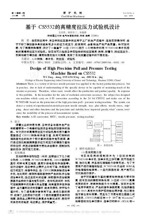
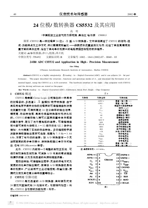
第30卷第4期2009年 4月煤 矿 机 械CoalM ine MachineryVol.30No.4Ap r.2009基于CS5532的高精度拉压力试验机设计吴房胜,欧阳名三,朱敏静(安徽理工大学电气与信息学院,安徽淮南232001) 摘 要:在实际应用中,有各种抗拉压器件被应用于工厂的生产流程中,但在实际操作时,由于不够了解该器件具体能承受多大的拉力或压力,故使用时,会影响生产和产品质量。
针对该问题,为了提高转换精度,设计了一套基于24位CS5532进行A/D转换并利用W78E516B单片机控制的高精度拉压力试验机。
该系统可以检测各种实验物的抗拉压强度、撕裂、胶着力、抗拉压应力、剥离和剪力等功能,精度和稳定性大大提高,克服了系统测量过程中的不稳定性。
关键词:A/D转换;单片机;抗拉压;试验机中图分类号:TP31;TG35 文献标志码:A 文章编号:1003-0794(2009)04-0192-03 Desi gn of Hi gh Precisi on Pull and Pressure Testi n gMachi n e Based on CS5532W U Fang-sheng,O UYANG M i n g-s an,ZHU M i n-ji n g(College of Electric Engineering Anhui University of Science and Technol ogy,Huainan232001,China) Abstract:There is a variety of devices tensile p ressure was app lied t o the fact ory p r oducti on p r ocess,but in p ractice,due t o lack of understanding of the s pecific device t o be capable of sustaining much of the tensi on or p ressure.Theref ore,when used,would affect the p r oducti on and p r oduct quality.I n res ponse t o this p r oble m.I n the meanti m e for the sake of exaltati on conversi on accuracy,the subject has designed one machine which carry on A/D conversi on according t o the24bit CS5532and make use of the W78E516B based on the p r otecti on of the high p recisi on pull-p ressure testing machine.The syste m can detect a variety of experi m ental materials p ressure tensile strength,tear,glue efforts,tensile stress,stri p2 p ing,shear and other functi ons and the p recisi on and stability have i m p r oved greatly,what’s more,over2 co me the instability of the p r ocess of measure ment syste m.Key words:A/D conversi on;MCU;tensile p ressure;testing machine0 前言随着工业的快速发展,各种设备与器件生产出来都需要有一个完善的检测设备来检测该器件的性能。
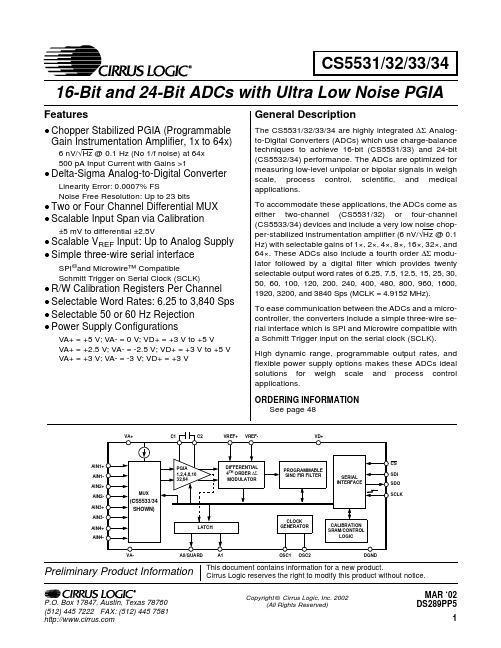
Copyright ©Cirrus Logic,Inc.200278760CS5531/32/33/3416-Bit and 24-Bit ADCs with Ultra Low Noise PGIAMAR ‘02TABLE OF CONTENTS1.CHARACTERISTICS AND SPECIFICATIONS (5)ANALOG CHARACTERISTICS (5)TYPICAL RMS NOISE(NV),CS5531/32/33/34-AS (8)TYPICAL NOISE FREE RESOLUTION(BITS),CS5532/34-AS (8)TYPICAL RMS NOISE(NV),CS5532/34-BS (9)TYPICAL NOISE FREE RESOLUTION(BITS),CS5532/34-BS (9)5V DIGITAL CHARACTERISTICS (10)3V DIGITAL CHARACTERISTICS (10)DYNAMIC CHARACTERISTICS (11)ABSOLUTE MAXIMUM RATINGS (11)SWITCHING CHARACTERISTICS (12)2.GENERAL DESCRIPTION (14)2.1.Analog Input (14)2.1.1.Analog Input Span (15)2.1.2.Multiplexed Settling Limitations (15)2.1.3.Voltage Noise Density Performance (15)2.1.4.No Offset DAC (15)2.2.Overview of ADC Register Structure and Operating Modes (16)2.2.1.System Initialization (17)mand Register Quick Reference (19)mand Register Descriptions (20)2.2.4.Serial Port Interface (24)2.2.5.Reading/Writing On-Chip Registers (25)2.3.Configuration Register (25)2.3.1.Power Consumption (25)2.3.2.System Reset Sequence (25)2.3.3.Input Short (26)2.3.4.Guard Signal (26)2.3.5.Voltage Reference Select (26)2.3.6.Output Latch Pins (26)2.3.7.Offset and Gain Select (27)Contacting Cirrus Logic SupportFor a complete listing of Direct Sales,Distributor,and Sales Representative contacts,visit the Cirrus Logic web site at: /corporate/contacts/sales.cfmSPI is a registered trademark of International Business Machines Corporation.Microwire is a trademark of National Semiconductor Corporation.IMPORTANT NOTICE"Preliminary"product information describes products that are in production,but for which full characterization data is not yet available."Advance"product infor-mation describes products that are in development and subject to development changes.Cirrus Logic,Inc.and its subsidiaries("Cirrus")believe that the infor-mation contained in this document is accurate and reliable.However,the information is subject to change without notice and is provided"AS IS"without warranty of any kind(express or implied).Customers are advised to obtain the latest version of relevant information to verify,before placing orders,that information being relied on is current and complete.All products are sold subject to the terms and conditions of sale supplied at the time of order acknowledgment,including those pertaining to warranty,patent infringement,and limitation of liability.No responsibility is assumed by Cirrus for the use of this information,including use of this information as the basis for manufacture or sale of any items,or for infringement of patents or other rights of third parties.This document is the property of Cirrus and by furnishing this information,Cirrus grants no license,express or implied under any patents,mask work rights,copyrights,trademarks,trade secrets or other intellectual property rights.Cirrus owns the copyrights of the information contained herein and gives consent for copies to be made of the information only for use within your organization with respect to Cirrus integrated circuits or other parts of Cirrus.This consent does not extend to other copying such as copying for general distribution,advertising or promotional purposes,or for creating any work for resale.An export permit needs to be obtained from the competent authorities of the Japanese Government if any of the products or technologies described in this ma-terial and controlled under the"Foreign Exchange and Foreign Trade Law"is to be exported or taken out of Japan.An export license and/or quota needs to be obtained from the competent authorities of the Chinese Government if any of the products or technologies described in this material is subject to the PRC Foreign Trade Law and is to be exported or taken out of the PRC.CERTAIN APPLICATIONS USING SEMICONDUCTOR PRODUCTS MAY INVOLVE POTENTIAL RISKS OF DEATH,PERSONAL INJURY,OR SEVERE PROPERTY OR ENVIRONMENTAL DAMAGE("CRITICAL APPLICATIONS").CIRRUS PRODUCTS ARE NOT DESIGNED,AUTHORIZED,OR WARRANT-ED TO BE SUITABLE FOR USE IN LIFE-SUPPORT DEVICES OR SYSTEMS OR OTHER CRITICAL APPLICATIONS.INCLUSION OF CIRRUS PRODUCTS IN SUCH APPLICATIONS IS UNDERSTOOD TO BE FULLY AT THE CUSTOMER'S RISK.Cirrus Logic,Cirrus,and the Cirrus Logic logo designs are trademarks of Cirrus Logic,Inc.All other brand and product names in this document may be trade-marks or service marks of their respective owners.2.3.8.Filter Rate Select (27)2.3.9.Configuration Register Descriptions (28)2.4.Setting up the CSRs for a Measurement (29)2.4.1.Channel-Setup Register Descriptions (30)2.5.Calibration (32)2.5.1.Calibration Registers (32)2.5.2.Gain Register (32)2.5.3.Offset Register (32)2.5.4.Performing Calibrations (33)2.5.5.Self Calibration (33)2.5.6.System Calibration (34)2.5.7.Calibration Tips (34)2.5.8.Limitations in Calibration Range (35)2.6.Performing Conversions (35)2.6.1.Single Conversion Mode (35)2.6.2.Continuous Conversion Mode (36)2.6.3.Examples of Using CSRs to Perform Conversions and Calibrations (37)ing Multiple ADCs Synchronously (38)2.8.Conversion Output Coding (38)2.8.1.Conversion Data Output Descriptions (39)2.9.Digital Filter (40)2.10.Clock Generator (41)2.11.Power Supply Arrangements (41)2.12.Getting Started (45)2.13.PCB Layout (45)3.PIN DESCRIPTIONS (46)Clock Generator (46)Control Pins and Serial Data I/O (46)Measurement and Reference Inputs (47)Power Supply Connections (47)4.SPECIFICATION DEFINITIONS (48)5.ORDERING GUIDE (48)6.PACKAGE DRAWINGS (49)LIST OF FIGURESFigure1.SDI Write Timing(Not to Scale) (13)Figure2.SDO Read Timing(Not to Scale) (13)Figure3.Multiplexer Configuration (14)Figure4.Input models for AIN+and AIN-pins (15)Figure5.Measured Voltage Noise Density (15)Figure6.CS5531/32/33/34Register Diagram (16)mand and Data Word Timing (24)Figure8.Guard Signal Shielding Scheme (26)Figure9.Input Reference Model when VRS=1 (27)Figure10.Input Reference Model when VRS=0 (27)Figure11.Self Calibration of Offset (34)Figure12.Self Calibration of Gain (34)Figure13.System Calibration of Offset (34)Figure14.System Calibration of Gain (34)Figure15.Synchronizing Multiple ADCs (38)Figure16.Digital Filter Response(Word Rate=60Sps) (40)Figure17.120Sps Filter Magnitude Plot to120Hz (40)Figure18.120Sps Filter Phase Plot to120Hz (40)Figure19.Z-Transforms of Digital Filters (40)Figure20.On-chip Oscillator Model (41)Figure21.CS5532Configured with a Single+5V Supply (42)Figure22.CS5532Configured with±2.5V Analog Supplies (43)Figure23.CS5532Configured with±3V Analog Supplies (43)Figure24.CS5532Configured for Thermocouple Measurement (44)Figure25.Bridge with Series Resistors (44)LIST OF TABLESTable1.Conversion Timing for Single Mode (36)Table2.Conversion Timing for Continuous Mode (37)mand Byte Pointer (37)Table4.Output Coding for16-bit CS5531and CS5533 (39)Table5.Output Coding for24-bit CS5532and CS5534 (39)1.CHARACTERISTICS AND SPECIFICATIONSANALOG CHARACTERISTICS(VA+,VD+=5V ±5%;VREF+=5V;VA-,VREF-,DGND =0V;MCLK =4.9152MHz;OWR (Output Word Rate)=60Sps;Bipolar Mode;Gain =32)(See Notes 1and 2.)Notes: 1.Applies after system calibration at any temperature within -40°C ~+85°C.2.Specifications guaranteed by design,characterization,and/or test.LSB is 16bits for the CS5531/33andLSB is 24bits for the CS5532/34.3.This specification applies to the device only and does not include any effects by external parasiticthermocouples.The PGIA contributes 5nV of offset drift,and the modulator contributes 640/G nV of offset drift,where G is the amplifier gain setting.4.Drift over specified temperature range after calibration at power-up at 25°C.ParameterCS5531-AS/CS5533-ASUnit Min Typ Max Accuracy Linearity Error -±0.0015±0.003%FS No Missing Codes 16--Bits Bipolar Offset -±1±2LSB 16Unipolar Offset-±2±4LSB 16Offset Drift(Notes 3and 4)-640/G +5-nV/°C Bipolar Full Scale Error -±8±31ppm Unipolar Full Scale Error -±16±62ppm Full Scale Drift(Note 4)-2-ppm/°CParameterCS5532-AS/CS5534-ASCS5532-BS/CS5534-BS Unit Min Typ Max Min Typ Max Accuracy Linearity Error -±0.0015±0.003-±0.0007±0.0015%FS No Missing Codes 24--24--Bits Bipolar Offset -±16±32-±16±32LSB 24Unipolar Offset-±32±64-±32±64LSB 24Offset Drift(Notes 3and 4)-640/G +5--640/G +5-nV/°C Bipolar Full Scale Error -±8±31-±8±31ppm Unipolar Full Scale Error -±16±62-±16±62ppm Full Scale Drift(Note 4)-TBD--2-ppm/°CANALOG CHARACTERISTICS(Continued)(See Notes 1and 2.)Notes: 5.The voltage on the analog inputs is amplified by the PGIA,and becomes V CM ±Gain*(AIN+-AIN-)/2atthe differential outputs of the amplifier.In addition to the input common mode +signal requirements for the analog input pins,the differential outputs of the amplifier must remain between (VA-+0.1V)and (VA+-0.1V)to avoid saturation of the output stage.6.See the section of the data sheet which discusses input models.ParameterMinTypMaxUnitAnalog InputCommon Mode +Signal on AIN+or AIN-Bipolar/Unipolar ModeGain =1Gain =2,4,8,16,32,64(Note 5)VA-VA-+0.7--VA+VA+-1.7V V CVF Current on AIN+or AIN-Gain =1(Note 6)Gain =2,4,8,16,32,64--500500--nA pA Input Current Noise Gain =1Gain =2,4,8,16,32,64--2001--pA/√Hz pA/√Hz Input Leakage for Mux when Off (at 25°C)-10-pA Off-Channel Mux Isolation -120-dB Open Circuit Detect Current 100300-nA Common Mode Rejection dc,Gain =1dc,Gain =6450,60Hz ---90130120---dB dB dB Input Capacitance -60-pF Guard Drive Output -20-µA Voltage Reference Input Range (VREF+)-(VREF-)1 2.5(VA+)-(VA-)V CVF Current (Note 6)-500-nA Common Mode Rejection dc 50,60Hz --120120--dB dB Input Capacitance 11-22pF System Calibration Specifications Full Scale Calibration Range Bipolar/Unipolar Mode 3-110%FS Offset Calibration Range Bipolar Mode -100-100%FS Offset Calibration Range Unipolar Mode -90-90%FSANALOG CHARACTERISTICS(Continued)(See Notes 1and 2.)7.All outputs unloaded.All input CMOS levels.8.Power is specified when the instrumentation amplifier (Gain ≥2)is on.Analog supply current is reducedby approximately 1/2when the instrumentation amplifier is off (Gain =1).9.Tested with 100mV change on VA+or VA-.ParameterCS5531/32/33/34-AS CS5532/34-BS MinTypMaxMinTypMaxUnitPower SuppliesDC Power Supply Currents (Normal Mode)I A+,I A-I D+--60.581--130.5151mA mA Power ConsumptionNormal Mode (Notes 7and 8)Standby Sleep---35350045-----70450080--mW mW µW Power Supply Rejection(Note 9)dc Positive Supplies dc Negative Supply--115115----115115--dB dBTYPICAL RMS NOISE (nV),CS5531/32/33/34-AS (See notes 10,11and 12)Notes:10.Wideband noise aliased into the baseband.Referred to the input.Typical values shown for 25°C.11.For Peak-to-Peak Noise multiply by 6.6for all ranges and output rates.12.Word rates and -3dB points with FRS =0.When FRS =1,word rates and -3dB points scale by 5/6.TYPICAL NOISE FREE RESOLUTION(BITS),CS5532/34-AS (See Notes 13and 14)13.Noise Free Resolution listed is for Bipolar operation,and is calculated as LOG((Input Span)/(6.6xRMSNoise))/LOG(2)rounded to the nearest bit.For Unipolar operation,the input span is 1/2as large,so one bit is lost.The input span is calculated in the analog input span section of the data sheet.The Noise Free Resolution table is computed with a value of 1.0in the gain register.Values other than 1.0will scale the noise,and change the Noise Free Resolution accordingly.14.“Noise Free Resolution”is not the same as “Effective Resolution”.Effective Resolution is based on theRMS noise value,while Noise Free Resolution is based on a peak-to-peak noise value specified as 6.6times the RMS noise value.Effective Resolution is calculated as LOG((Input Span)/(RMS Noise))/LOG(2).Specifications are subject to change without notice.Output Word Rate (Sps)-3dB Filter Frequency (Hz)Instrumentation Amplifier Gain x64x32x16x8x4x2x17.5 1.9417171926427915515 3.882425273659111218307.7534353951841573086015.548495472118222436120316870771021673146162406211516027652710402070415048012216323039274814802950589096023022932155410602090417083401,920390344523946184036507290146003,84078013902710539010800215004300086100Output Word Rate (Sps)-3dB Filter Frequency (Hz)Instrumentation Amplifier Gain x64x32x16x8x4x2x17.5 1.941920212222222215 3.8819202121212222307.75181920212121216015.5181920202021211203117181920202020240621617171717171748012216171717171717960230151616161616161,920390151515151515153,84078013131313131313TYPICAL RMS NOISE (nV),CS5532/34-BS (See notes 15,16,17and 18)Notes:15.The -B devices provide the best noise specifications.16.Wideband noise aliased into the baseband.Referred to the input.Typical values shown for 25°C.17.For Peak-to-Peak Noise multiply by 6.6for all ranges and output rates.18.Word rates and -3dB points with FRS =0.When FRS =1,word rates and -3dB points scale by 5/6.TYPICAL NOISE FREE RESOLUTION(BITS),CS5532/34-BS (See Notes 19and 20)19.Noise Free Resolution listed is for Bipolar operation,and is calculated as LOG((Input Span)/(6.6xRMSNoise))/LOG(2)rounded to the nearest bit.For Unipolar operation,the input span is 1/2as large,so one bit is lost.The input span is calculated in the analog input span section of the data sheet.The Noise Free Resolution table is computed with a value of 1.0in the gain register.Values other than 1.0will scale the noise,and change the Noise Free Resolution accordingly.20.“Noise Free Resolution”is not the same as “Effective Resolution”.Effective Resolution is based on theRMS noise value,while Noise Free Resolution is based on a peak-to-peak noise value specified as 6.6times the RMS noise value.Effective Resolution is calculated as LOG((Input Span)/(RMS Noise))/LOG(2).Specifications are subject to change without notice.Output Word Rate (Sps)-3dB Filter Frequency (Hz)Instrumentation Amplifier Gain x64x32x16x8x4x2x17.5 1.948.59101526509915 3.88121315213770139307.751718213052991966015.524252942731402771203134364259103198392240628013626051410202050409048012211319436973014502900581096023015927452310302060411082301,920390260470912181036207230145003,84078013602690538010800215004300086000Output Word Rate (Sps)-3dB Filter Frequency (Hz)Instrumentation Amplifier Gain x64x32x16x8x4x2x17.5 1.942021222323232315 3.8820212222222222307.75192021222222226015.5192021212121211203118192021212121240621717181818181848012217171717171717960230161617171717171,920390161616161616163,840780131313131313135V DIGITAL CHARACTERISTICS (VA+,VD+=5V ±5%;VA-,DGND =0V;See Notes 2and 21.)3V DIGITAL CHARACTERISTICS (T A =25°C;VA+=5V ±5%;VD+=3.0V±10%;VA-,DGND =0V;See Notes 2and 21.)21.All measurements performed under static conditions.ParameterSymbol Min Typ Max Unit High-Level Input Voltage All Pins Except SCLKSCLK V IH 0.6VD+(VD+)-0.45--VD+VD+V Low-Level Input Voltage All Pins Except SCLKSCLK V IL 0.00.0-0.80.6V High-Level Output Voltage A0and A1,I out =-1.0mASDO,I out =-5.0mA V OH (VA+)-1.0(VD+)-1.0--V Low-Level Output Voltage A0and A1,I out =1.0mASDO,I out =5.0mAV OL --(VA-)+0.40.4V Input Leakage Current I in -±1±10µA SDO 3-State Leakage Current I OZ --±10µA Digital Output Pin CapacitanceC out-9-pFParameterSymbol Min Typ Max Unit High-Level Input Voltage All Pins Except SCLKSCLK V IH 0.6VD+(VD+)-0.45-VD+VD+V Low-Level Input Voltage All Pins Except SCLKSCLK V IL 0.00.0-0.80.6V High-Level Output Voltage A0and A1,I out =-1.0mASDO,I out =-5.0mA V OH (VA+)-1.0(VD+)-1.0--V Low-Level Output Voltage A0and A1,I out =1.0mASDO,I out =5.0mAV OL --(VA-)+0.40.4V Input Leakage Current I in -±1±10µA SDO 3-State Leakage Current I OZ --±10µA Digital Output Pin CapacitanceC out-9-pFDYNAMIC CHARACTERISTICS22.The ADCs use a Sinc 5filter for the 3200Sps and 3840Sps output word rate (OWR)and a Sinc 5filterfollowed by a Sinc 3filter for the other OWRs.OWR sinc5refers to the 3200Sps (FRS =1)or 3840Sps (FRS =0)word rate associated with the Sinc 5filter.23.The single conversion mode only outputs fully settled conversions.See Table 1for more details aboutsingle conversion mode timing.OWR SC is used here to designate the different conversion time associated with single conversions.24.The continuous conversion mode outputs every conversion.This means that the filter’s settling timewith a full scale step input in the continuous conversion mode is dictated by the OWR.ABSOLUTE MAXIMUM RATINGS(DGND =0V;See Note 25.)Notes:25.All voltages with respect to ground.26.VA+and VA-must satisfy {(VA+)-(VA-)}≤+6.6V.27.VD+and VA-must satisfy {(VD+)-(VA-)}≤ +7.5V.28.Applies to all pins including continuous overvoltage conditions at the analog input (AIN)pins.29.Transient current of up to 100mA will not cause SCR latch-up.Maximum input current for a power supply pin is ±50mA.30.Total power dissipation,including all input currents and output currents.WARNING:Operation at or beyond these limits may result in permanent damage to the device.Normal operation is not guaranteed at these extremes.ParameterSymbol Ratio Unit Modulator Sampling Ratef s MCLK/16Sps Filter Settling Time to 1/2LSB (Full Scale Step Input)Single Conversion mode (Notes 22,23,and 24)Continuous Conversion mode,OWR <3200Sps Continuous Conversion mode,OWR ≥3200Spst s t s t s1/OWR SC5/OWR sinc5+3/OWR5/OWRs s sParameterSymbolMin Typ Max Unit DC Power Supplies(Notes 26and 27)Positive Digital Positive Analog Negative Analog VD+VA+VA--0.3-0.3+0.3---+6.0+6.0-3.75V V V Input Current,Any Pin Except Supplies (Notes 28and 29)I IN --±10mA Output Current I OUT --±25mA Power Dissipation (Note 30)PDN --500mW Analog Input Voltage VREF pins AIN PinsV INR V INA (VA-)-0.3(VA-)-0.3--(VA+)+0.3(VA+)+0.3V V Digital Input VoltageV IND -0.3-(VD+)+0.3V Ambient Operating Temperature T A -40-85°C Storage T emperature T stg-65-150°CSWITCHING CHARACTERISTICS (VA+=2.5V or 5V ±5%;VA-=-2.5V±5%or 0V;VD+=3.0V±10%or 5V ±5%;DGND =0V;Levels:Logic 0=0V,Logic 1=VD+;C L =50pF;See Figures 1and 2.)Notes:31.Device parameters are specified with a 4.9152MHz clock.32.Specified using 10%and 90%points on waveform of interest.Output loaded with 50pF.33.Oscillator start-up time varies with crystal parameters.This specification does not apply when using anexternal clock source.ParameterSymbol MinTypMaxUnitMaster Clock Frequency (Note 31)External Clock or Crystal OscillatorMCLK1 4.91525MHz Master Clock Duty Cycle 40-60%Rise Times(Note 32)Any Digital Input Except SCLKSCLKAny Digital Output t rise-----50 1.0100-µs µs ns Fall Times(Note 32)Any Digital Input Except SCLKSCLKAny Digital Output t fall-----50 1.0100-µs µs ns Start-upOscillator Start-up Time XTAL =4.9152MHz(Note 33)t ost-20-ms Serial Port Timing Serial Clock Frequency SCLK 0-2MHz Serial Clock Pulse Width High Pulse Width Lowt 1t 2250250----ns nsSDI Write TimingCS Enable to Valid Latch Clock t 350--ns Data Set-up Time prior to SCLK rising t 450--ns Data Hold Time After SCLK Rising t 5100--ns SCLK Falling Prior to CS Disable t 6100--nsSDO Read Timing CS to Data Validt 7--150ns SCLK Falling to New Data Bit t 8--150ns CS Rising to SDO Hi-Zt 9--150nsFigure1.SDI Write Timing(Not toScale)2.GENERAL DESCRIPTIONThe CS5531/32/33/34are highly integrated∆ΣAn-alog-to-Digital Converters(ADCs)which use charge-balance techniques to achieve16-bit (CS5531/33)and24-bit(CS5532/34)performance. The ADCs are optimized for measuring low-level unipolar or bipolar signals in weigh scale,process control,scientific,and medical applications.To accommodate these applications,the ADCs come as either two-channel(CS5531/32)or four-channel(CS5533/34)devices and include a very low noise chopper-stabilized programmable gain instrumentation amplifier(PGIA,6nV/√Hz@0.1 Hz)with selectable gains of1×,2×,4×,8×,16×, 32×,and64×.These ADCs also include a fourth or-der∆Σmodulator followed by a digital filter which provides twenty selectable output word rates of6.25, 7.5,12.5,15,25,30,50,60,100,120,200,240,400, 480,800,960,1600,1920,3200,and3840Samples per second(MCLK=4.9152MHz).To ease communication between the ADCs and a micro-controller,the converters include a simple three-wire serial interface which is SPI and Mi-crowire compatible with a Schmitt Trigger input on the serial clock(SCLK).2.1.Analog InputFigure3illustrates a block diagram of the CS5531/32/33/34.The front end consists of a multi-plexer,a unity gain coarse/fine charge input buffer, and a programmable gain chopper-stabilized instru-mentation amplifier.The unity gain buffer is activat-ed any time conversions are performed with a gain of one and the instrumentation amplifier is activated any time conversions are performed with gain set-tings greater than one.The unity gain buffer is designed to accommodate rail to rail input signals.The common-mode plus signal range for the unity gain buffer amplifier is VA-to VA+.Typical CVF(sampling)current for the unity gain buffer amplifier is about500nA (MCLK=4.9152MHz,see Figure4).The instrumentation amplifier is chopper-stabi-lized and operates with a chop clock frequency of MCLK/128.The CVF(sampling)current into the instrumentation amplifier is typically500pA overFigure3.Multiplexer Configuration-40°C to+85°C(MCLK=4.9152MHz).The com-mon-mode plus signal range of the instrumentation amplifier is(VA-)+0.7V to(VA+)-1.7V. Figure4illustrates the input models for the ampli-fiers.The dynamic input current for each of the pins can be determined from the models shown. Note:The C=2.5pF and C=16pF capacitors are for input current modeling only.For physicalinput capacitance see‘Input Capacitance’specification under Analog Characteristics.2.1.1.Analog Input SpanThe full scale input signal that the converter can dig-itize is a function of the gain setting and the refer-ence voltage connected between the VREF+and VREF-pins.The full scale input span of the convert-er is((VREF+)-(VREF-))/(GxA),where G is the gain of the amplifier and A is2for VRS=0,or A is 1for VRS=1.VRS is the Voltage Reference Select bit,and must be set according to the differential volt-age applied to the VREF+and VREF-pins on the part.See section2.3.5for more details.After reset,the unity gain buffer is engaged.With a 2.5V reference this would make the full scale input range default to2.5V.By activating the instrumen-tation amplifier(i.e.a gain setting other than1)and using a gain setting of32,the full scale input range can quickly be set to2.5/32or about78mV.Note that these input ranges assume the calibration regis-ters are set to their default values(i.e.Gain=1.0and Offset=0.0).2.1.2.Multiplexed Settling LimitationsThe settling performance of the CS5531/32/33/34 in multiplexed applications is affected by the sin-gle-pole low-pass filter which follows the instru-mentation amplifier(see Figure3).To achieve data sheet settling and linearity specifications,it is rec-ommended that a22nF C0G capacitor be used.Ca-pacitors as low as10nF or X7R type capacitors can also be used with some minor increase in distortion for AC signals.2.1.3.Voltage Noise Density Performance Figure5illustrates the measured voltage noise den-sity versus frequency from0.01Hz to10Hz of a CS5532-BS.The device was powered with±2.5V supplies,using120Sps OWR,the64x gain range, bipolar mode,and with the input short bit enabled.2.1.4.No Offset DACAn offset DAC was not included in the CS553X family because the high dynamic range of the con-verter eliminates the need for one.The offset regis-Figure4.Input models for AIN+and AIN-pinster can be manipulated by the user to mimic the function of a DAC if desired.2.2.Overview of ADC Register Structure and Operating ModesThe CS5531/32/33/34ADCs have an on-chip con-troller,which includes a number of user-accessible registers.The registers are used to hold offset and gain calibration results,configure the chip's operat-ing modes,hold conversion instructions,and to store conversion data words.Figure6depicts a block diagram of the on-chip controller’s internal registers.Each of the converters has32-bit registers to func-tion as offset and gain calibration registers for each channel.The converters with two channels have two offset and two gain calibration registers,the converters with four channels have four offset and four gain calibration registers.These registers hold calibration results.The contents of these registers can be read or written by the user.This allows cal-ibration data to be off-loaded into an external EE-PROM.The user can also manipulate the contents of these registers to modify the offset or the gain slope of the converter.The converters include a32-bit configuration reg-ister which is used for setting options such as the power down modes,resetting the converter,short-ing the analog inputs,and enabling diagnostic test bits like the guard signal.A group of registers,called Channel Setup Regis-ters,are used to hold pre-loaded conversion in-structions.Each channel setup register is32bits long,and holds two16-bit conversion instructions referred to as Setups.Upon power up,these regis-ters can be initialized by the system microcontrol-ler with conversion instructions.The user can then instruct the converter to perform single or multiple conversions or calibrations with the converter in the mode defined by one of these Setups.Figure6.CS5531/32/33/34Register DiagramUsing the single conversion mode,an8-bit com-mand word can be written into the serial port.The command includes pointer bits which‘point’to a 16-bit command in one of the Channel Setup Reg-isters which is to be executed.The16-bit Setups can be programmed to perform a conversion on any of the input channels of the converter.More than one of the16-bit Setups can be used for the same analog input channel.This allows the user to con-vert on the same signal with either a different con-version speed,a different gain range,or any of the other options available in the channel setup regis-ters.Alternately,the user can set up the registers to perform different conversion conditions on each of the input channels.The ADCs also include continuous conversion ca-pability.The ADCs can be instructed to continu-ously convert,referencing one16-bit command Setup.In the continuous conversions mode,the conversion data words are loaded into a shift regis-ter.The converter issues a flag on the SDO pin when a conversion cycle is completed so the user can read the register,if need be.See the section on Performing Conversions for more details.The following pages document how to initialize the converter,perform offset and gain calibrations,and how to configure the converter for the various con-version modes.Each of the bits of the configuration register and of the Channel Setup Registers is de-scribed.A list of examples follows the description section.Also the Command Register Quick Refer-ence can be used to decode all valid commands(the first8-bits into the serial port).2.2.1.System InitializationThe CS5531/32/33/34provide no power-on-reset function.To initialize the ADCs,the user must per-form a software reset by resetting the ADC’s serial port with the Serial Port Initialization sequence. This sequence resets the serial port to the command mode and is accomplished by transmitting at least 15SYNC1command bytes(0xFF hexadecimal),followed by one SYNC0command(0xFE hexa-decimal).Note that this sequence can be initiated at anytime to reinitialize the serial port.To complete the system initialization sequence,the user must also perform a system reset sequence which is as follows:Write a logic1into the RS bit of the con-figuration register.This will reset the calibration registers and other logic(but not the serial port).A valid reset will set the RV bit in the configuration register to a logic1.After writing the RS bit to a logic1,wait20microseconds,then write the RS bit back to logic0.While this involves writing an en-tire word into the configuration register,the RV bit is a read only bit,therefore a write to the configu-ration register will not overwrite the RV bit.After clearing the RS bit back to logic0,read the config-uration register to check the state of the RV bit as this indicates that a valid reset occurred.Reading the configuration register clears the RV bit back to logic0.Completing the reset cycle initializes the on-chip registers to the following states:Note:Previous datasheets stated that the RS bit would clear itself back to logic0and thereforethe user was not required to write the RS bitback to logic0.The current data sheetinstruction that requires the user to write intothe configuration register to clear the RS bithas been added to insure that the RS bit iscleared.Characterization across multiple lotsof silicon has indicated some chips do notautomatically reset the RS bit to logic0in theconfiguration register,although the resetfunction is completed.This occurs only onsmall number of chips when the VA-supply isnegative with respect to DGND.This has notcaused an operational issue for customersbecause their start-up sequence includeswriting a word(with RS=0)into theconfiguration register after performing areset.The change in the reset sequence to Configuration Register:00000000(H)Offset Registers:00000000(H)Gain Registers:01000000(H)Channel Setup Registers:00000000(H)。

⽹友⽤的芯⽚总结⽹友⽤的芯⽚总结(整理版)⽹友在各⾃领域中所⽤到的芯⽚总结1.⾳频pcm编码DA转换芯⽚cirrus logic的cs4344,cs43344334是⽼封装,据说已经停产,4344封装⽐较⼩,⾮常好⽤。
还有菲利谱的。
8211等。
2.⾳频放⼤芯⽚4558,833,此⼆芯⽚都是双运放。
为什么不⽤324等运放个⼈觉得应该是对⾳频的频率响应⽐较好。
3.244和245,由于244是单向a=b的所以只是单向驱动。
⽽245是⽤于数据总线等双向驱动选择。
同时245的封装⾛线⾮常适合数据总线,它按照顺序d7-d0。
4.373和374,地址锁存器,⼀个电平触发,⼀个沿触发。
373⽤在单⽚机p0地址锁存,当然是扩展外部ram的时候⽤到62256。
374有时候也⽤在锁数码管内容显⽰。
5.max232和max202,有些为了节约成本就⽤max202,主要是驱动能⼒的限制。
6.⽹络接⼝变压器。
需要注意差分信号的等长和尽量短的规则。
7.amd29系列的flash,有bottom型和top型,主要区别是loader区域设置在哪⾥?bottom型的在开始地址空间,top型号的在末尾地址空间,我感觉有点反,但实际就是这么命名的。
8.164,它是⼀个串并转换芯⽚,可以把串⾏信号变为并⾏信号,控制数码管显⽰可以⽤到。
9.sdram,ddrram,在设计时候通常会在数据地址总线上加22,33的电阻,据说是为了阻抗匹配,对于这点我理论基础学到过,但实际上没什么深刻理解。
10.⽹卡控制芯⽚ax88796,rtl8019as,dm9000ae当然这些都是⽤在isa总线上的。
11.24位AD:CS5532,LPC2413效果还可以12.仪表运放:ITL114,不过据说功耗有点⼤13、⾳频功放:⼀般⽤LM36814、⾳量控制IC. PT2257/9.15.PCM双向解/编码 ADC/DAC CW669116.2.4G双⼯通讯 RF IC CC250017.cat809,max809,这些是电源监控芯⽚,当低于某⼀电压以后⽐如3.07v等出现⼀个100ms的低电平,实现复位功能。
KX3552驱动在window7 64位下安装教程1、先卸载老版软件。
点所有程序—kx AudioDriver--uninstall kX Project audio driver进行卸载卸载后重启系统2、先安装 vcredist_x86 安装包里面有!3、设置主驱动以管理员身份运行如下图:并安装专用kx3552驱动、关闭杀软和禁用Windows Defender服务左下角任务栏处右键“运行”输入services.msc,弹出“服务”窗口,在名称一栏中找到Windows Defender,右击,选“属性”,启动类型中选择“禁用”,确定。
1 / 15继续安装2 / 15见到下面提示,不需要重新启动。
继续安装3 / 15如果见到下面提示不要理会,继续安装。
3、将C:\Program Files\kX Project\下面的kx.inf和kx.sys 复制到系系统盘的windows和windows下的system32目录下。
4 / 154、打开控制面版,打开设备管理器。
5 / 15点多媒体音频管理器(你的可能是其他有问题的音频硬件),右键,点更新驱动程序软件。
点浏览计算机以查找驱动程序软件6 / 15点从计算机的设备驱动程序列表中选择(L)7 / 15选声音、视频和游戏控制器,下一步。
8 / 15点从磁盘安装(H)9 / 1510 / 15选系统winows\systm32目录下kx.inf文件。
稍等一会儿出现如界面,祝贺你安装成功。
各种效果大11 / 15家一起探索吧。
12 / 15点右下角喇叭图标可见以下界面。
13 / 1514 / 15祝各位网友安装成功。
15 / 15。
密级学号毕业设计(论文)基于CS5532的高精度药品自动称重系统的研究院(系、部):信息工程学院姓名:年级:专业:测控技术与仪器指导教师:教师职称:讲师2013年06月15日·北京北京石油化工学院毕业设计(论文)任务书学院(系、部)信息工程学院专业班级学生姓名指导教师/职称1.毕业设计(论文)题目基于CS5532的高精度药品自动称重系统的研究2.任务起止日期: 2012年 12 月 12日至 2013年 06 月 22 日(含岗位实习)3.毕业设计(论文)的主要内容与要求(含原始数据及应提交的成果)具体工作任务与要求:翻译外文资料(不少于25000字符)技术调研提出高精度药品自动称重系统方案确定控制系统硬件总体方案及实现确定控制系统软件方案及实现预期培养目标:具备文献查阅与综合能力具备外文阅读与翻译能力具备数据收集、分析、计算和处理能力具备项目调研、设计及调试能力具备现场解决问题的能力具备一定的科技论文写作能力最终提交材料:外文资料原文(不少于25000字符)及翻译稿设计说明书系统硬件原理图系统软件流程图及代码4.主要参考文献图书馆藏嵌入式相关图书;cnki中国期刊全文数据库及万方数据库;5.进度计划及指导安排(前5周的内容安排在寒假前)任务书审定日期年月日系(教研室)主任(签字)任务书批准日期年月日教学院(系、部)院长(签字)任务书下达日期2012年12月12日指导教师(签字)计划完成任务日期2013年06月22日学生(签字)摘要随着计算机和测控技术的不断进步与发展,人们对称重系统的要求也越来越高,药品的包装现场,需要精确、操作简便和快速的称重装置。
本论文采用电阻应变片式压力传感器,被待测物施加了一个压力,导致传感器发生一定形变,从而使传感器阻抗产生改变,并使其电压产生改变,输出一个变化的模拟信号。
经放大电路放大该信号输出到CS5532(高精度24位A/D转换芯片,可实现传感器微弱信号的采集与转换,提高了系统的精度)将其转换成数字信号输出到核心控制器80C52。
电路图接线:
驱动程序:
//CS5532的驱动程序,
#include <c8051f020.h>
#include <intrins.h>
sbit NSS0=P3^0; //片选端在P3.0端口
sbit SDO=P0^3; //MISO连接到P0.3端口
#define CS5532_SELECT NSS0=0 // CS5532片选开#define CS5532_NOSELECT NSS0=1 // CS5532片选关
//切换到外部晶振11.0592MHZ
void Oscillator_Init()
{
int i = 0;
OSCXCN = 0x67;
for (i = 0; i < 3000; i++);
while ((OSCXCN & 0x80) == 0);
OSCICN = 0x08;
}
//延时,对于11.0592Mhz的晶振,1106延时0.1MS void delay_ms(unsigned int x)
{
unsigned int y;
while(x!=0)
{
x--;
for(y=0;y<=1106;y++);
}
}
//向cs5532写一个字节
void SendSPIByte(unsigned char ch)
{
SPIF = 0;
SPI0DAT = ch;
while (0==SPIF); // 等待写结束
SPIF = 0;
}
//cs5532向单片机发一个字节
unsigned char RecSPIByte(void)
{
unsigned char ch;
ch=0;
SPIF=0;
SPI0DAT=0;
while(0==SPIF);
ch=SPI0DAT;
// SPIF=0;
return(ch);
}
//cs5532复位
void CS5532Reset(void)
{
unsigned char i,recs[4];
for(i=0;i<4;i++)
{
recs[i]=0;
}
CS5532_SELECT;
for(i=0;i<15;i++) //5532初始化序列,芯片进入命令模式
{
SendSPIByte(0xff);
}
SendSPIByte(0xfe);
delay_ms(100);
SendSPIByte(0x03); //5532系统复位,RS=1,写配置寄存器
SendSPIByte(0x20);
SendSPIByte(0x00);
SendSPIByte(0x00);
SendSPIByte(0x00);
delay_ms(100);
while(recs[0]!=0x10) //等待复位(RV=1)完成,
{
SendSPIByte(0x0b); //读配置寄存器,直到bit RV=1
recs[0]=RecSPIByte();
recs[1]=RecSPIByte();
recs[2]=RecSPIByte();
recs[3]=RecSPIByte();
}
// CS5532_NOSELECT;
}
//CS5532初始化
void CS5532_init(void)
{
CS5532Reset();
delay_ms(100);
//设置配置寄存器
SendSPIByte(0x03); //配置寄存器命令字
SendSPIByte(0x02); //正常模式0V<VREF<=2.5V VRS=1
SendSPIByte(0x00); //实际参考电压4.96V,为了扩大测量电压范围VRS=1, SendSPIByte(0x00);
SendSPIByte(0x00);
//设置通道寄存器
delay_ms(100);
SendSPIByte(0x05); //通道寄存器命令字
SendSPIByte(0x02); //VRS=0 A=2; VRS=1 A=1;
SendSPIByte(0x40); //单极性模式、物理通道1、1倍增益单极性增益范围[(VREF+ - VREF-)]/1*A
SendSPIByte(0x02); //7.5Hz字速率执行转换只是用于连续转换模式SendSPIByte(0x40);
//设置增益寄存器
SendSPIByte(0x02); //增益寄存器命令字
SendSPIByte(0x01); //自增益增益1.0
SendSPIByte(0x00);
SendSPIByte(0x00);
SendSPIByte(0x00);
//设置偏移寄存器
delay_ms(100);
SendSPIByte(0x01); //偏移寄存器命令字
SendSPIByte(0x00); //自偏移偏移0.0
SendSPIByte(0x00);
SendSPIByte(0x00);
SendSPIByte(0x00);
//delay_ms(100);
//SendSPIByte(0x81); //自偏移
//delay_ms(100);
//SendSPIByte(0x82);//自增益
}
/*
//测试
unsigned char xdata buf[4];
unsigned long int value;
unsigned long int temp;
unsigned char i;
void main (void)
{
WDTCN = 0xde;
WDTCN = 0xad;
XBR0 = 0xDe;//UART0,SPI,SMBus连到端口
XBR1 = 0x04;//INT0连到端口
XBR2 = 0x40;//弱上拉允许,交叉开关允许,UART1连到端口
//SPI设定
SPI0CFG=0x07; //SCK第2个边沿采样,在空闲时处于低电平,贞长度8
SPI0CN= 0x03; //SPI主方式操作,SPI允许
SPI0CKR=0x02; //SPI时钟Fsck=(11.0592/2)/3=1.8342MHz
P0MDOUT = 0xf5;//P0口配置,各个端口输入时配置为漏极开路,输出时配置为推挽方式
P1MDOUT = 0x31;//P1口配置
P2MDOUT = 0xdd;//P2口配置
P3MDOUT = 0x5f;
P74OUT = 0xfc;//P7-4口配置
Oscillator_Init();
CS5532_init();
for(i=0;i<4;i++)
{
buf[i]=0;
}
value=0;
while(1)
{
//SendSPIByte(0x0d); //读通道寄存器
//SendSPIByte(0x09); //读偏移寄存器
//SendSPIByte(0x0a); //读增益寄存器
//SendSPIByte(0x0b); //读配置寄存器
SendSPIByte(0x80); //单次转换
//SendSPIByte(0xc0); //连续转换
while(SDO==1); //等待SDO置0
RecSPIByte(); //清标志位,等待读取8位数据的时间
buf[0]=RecSPIByte(); //读取32bit数据高位在前
buf[1]=RecSPIByte(); //
buf[2]=RecSPIByte(); //
buf[3]=RecSPIByte(); //末位04代表溢出
temp=buf[0];
temp=temp<<8;
temp+=buf[1];
temp=temp<<8;
temp+=buf[2];
value=temp; //转化电压范围0.8mV~4.12V
delay_ms(100);
}
}
*/。