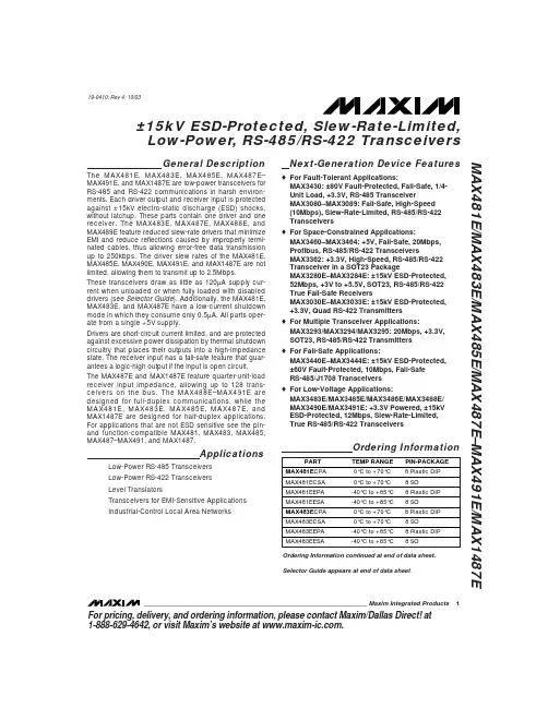
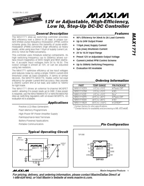
MAX5177BEEE+中文资料
- 格式:pdf
- 大小:260.39 KB
- 文档页数:16
ELECTRICAL CHARACTERISTICS—MAX5175
Applications
Digitally Programmable 4–20mA Current Loops Industrial Process Controls Digital Offset and Gain Adjustment Motion Control Automatic Test Equipment (ATE) Remote Industrial Controls µP-Controlled Systems
TOP VIEW
FB 1 OUT 2 RS 3 PDL 4 CLR 5 CS 6 DIN 7 SCLK 8
Pin Configuration
16 VDD 15 N.C. 14 REF
MAX5175 MAX5177
13 AGND 12 SHDN 11 UPO 10 DOUT 9 DGND
QSOP 1
________________________________________________________________ Maxim Integrated Products
Functional Diagram appears at end of data sheet. SPI and QSPI are trademarks of Motorola, Inc. MICROWIRE is a trademark of National Semiconductor Corp. Rail-to-Rail is a registered trademark of Nippon Motorola, Ltd.
元器件交易网
19-1477; Rev 0; 4/99
Low-Power, Serial, 12-Bit DACs with Force/Sense Voltage Output
General Description
The MAX5175/MAX5177 low-power, serial, voltage-output, 12-bit digital-to-analog converters (DACs) feature a precision output amplifier in a space-saving 16-pin QSOP package. The MAX5175 operates from a single +5V supply, and the MAX5177 operates from a single +3V supply. The output amplifier’s inverting input is available to allow specific gain configurations, remote sensing, and high output current capability. This makes the MAX5175/MAX5177 ideal for a wide range of applications, including industrial process control. Both devices draw only 260µA of supply current, which reduces to 1µA in shutdown mode. In addition, the programmable power-up reset feature allows for a userselectable output voltage state of either 0 or midscale. The 3-wire serial interface is compatible with SPI™, QSPI™, and MICROWIRE™ standards. An input register followed by a DAC register provides a double-buffered input, allowing the registers to be updated independently or simultaneously with a 16-bit serial word. Additional features include software and hardware shutdown, shutdown lockout, a hardware reset pin, and a reference input capable of accepting DC and offset AC signals. These devices provide a programmable digital output pin for added functionality and a serial-data output pin for daisy-chaining. All logic inputs are TTL/CMOS compatible and are internally buffered with Schmitt triggers to allow direct interfacing to optocouplers. The MAX5175/MAX5177 incorporate a proprietary on-chip circuit that keeps the output voltage virtually “glitch free,” limiting the glitches to a few millivolts during power-up. Both devices come in 16-pin QSOP packages and are specified for the extended (-40°C to +85°C) temperature range. The MAX5171/MAX5173 are 14-bit pin-compatible upgrades to the MAX5175/MAX5177. For pin-compatible DACs with an internal reference, see the 13-bit MAX5132/MAX5133 and 12-bit MAX5122/MAX5123. o ±1 LSB INL o 1µA Shutdown Current o “Glitch Free” Output Voltage at Power-Up o Single-Supply Operation +5V (MAX5175) +3V (MAX5177) o Full-Scale Output Range +2.048V (MAX5177, VREF = +1.25V) +4.096V (MAX5175, VREF = +2.5V) o Rail-to-Rail® Output Amplifier o Adjustable Output Offset o Low THD (-80dB) in Multiplying Operation o SPI/QSPI/MICROWIRE-Compatible 3-Wire Serial Interface o Programmable Shutdown Mode and Power-Up Reset (0 or midscale) o Buffered Output Capable of Driving 4–20mA or 5kΩ || 100pF Loads o User-Programmable Digital Output Pin Allows Serial Control of External Components o 14-Bit Upgrades Available (MAX5171/MAX5173)
Low-Power, Serial, 12-Bit DACs with Force/Sense Voltage Output MAX5175/MAX5177
ABSOLUTE MAXIMUM RATINGS
VDD to AGND, DGND ...............................................-0.3V to +6V AGND to DGND.....................................................-0.3V to +0.3V Digital Inputs to DGND.............................................-0.3V to +6V DOUT, UPO to DGND ................................-0.3V to (VDD + 0.3V) FB, OUT REF to AGND...............................-0.3V to (VDD + 0.3V) Maximum Current into Any Pin............................................50mA Continuous Power Dissipation (TA = +70°C) 16-Pin QSOP (derate 8mW/°C above +70°C)...............667mW Operating Temperature Range .............................-40°C to +85°C Storage Temperature Range .............................-65°C to +150°C Lead Temperature (soldering, 10sec) .............................+300°C