AD8354ACPZ-REEL7中文资料
- 格式:pdf
- 大小:489.85 KB
- 文档页数:16
GENERAL DESCRIPTION
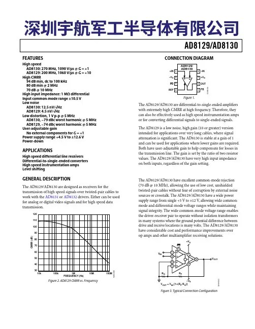
The AD8354 is a broadband, fixed-gain, linear amplifier that operates at frequencies from 1 MHz up to 2.7 GHz. It is intended for use in a wide variety of wireless devices, including cellular, broadband, CATV, and LMDS/MMDS applications. By taking advantage of ADI’s high performance, complementary Si bipolar process, these gain blocks provide excellent stability over process, temperature, and power supply. This amplifier is single-ended and internally matched to 50 Ω with a return loss of greater than 10 dB over the full operating frequency range. The AD8354 provides linear output power of nearly 4.3 dBm with 20 dB of gain at 900 MHz when biased at 3 V and an external RF choke is connected between the power supply and the output pin. The dc supply current is 24 mA. At 900 MHz, the output third-order intercept (OIP3) is greater than 18 dBm; at 2.7 GHz, the OIP3 is 14 dBm. The noise figure is 4.2 dB at 900 MHz. The reverse isolation (S12) is −33 dB at 900 MHz. The AD8354 can also operate with a 5 V power supply; in which case, no external inductor is required. Under these conditions, the AD8354 delivers 4.88 dBm with 20 dB of gain at 900 MHz. The dc supply current is 26 mA. At 900 MHz, the OIP3 is greater than 19 dBm; at 2.7 GHz, the OIP3 is 15 dBm. The noise figure is 4.4 dB at 900 MHz. The reverse isolation (S12) is −33 dB. The AD8354 is fabricated on ADI’s proprietary, high performance, 25 GHz, Si complementary, bipolar IC process. The AD8354 is available in a chip scale package that uses an exposed paddle for excellent thermal impedance and low impedance electrical connection to ground. It operates over a −40°C to +85°C temperature range, and an evaluation board is also available.
FUNCTIONAL BLOCK DIAGRAM
BIAS AND VREF
VPOS
INPT
VOUT
COM1
AD8354
Figure 1.
COM2
APPLICATIONS
VCO buffers General Tx/Rx amplification Power amplifier predrivers Low power antenna drivers
元器件交易网
1 MHz to 2.7 GHz RF Gain Block AD8354
FEATURES
Fixed gain of 20 dB Operational frequency of 1 MHz to 2.7 GHz Linear output power up to 4 dBm Input/output internally matched to 50 Ω Temperature and power supply stable Noise figure: 4.2 dB Power supply: 3 V or 5 V
Rev. C
Information furnished by Analog Devices is believed to be accurate and reliable. However, no responsibility is assumed by Analog Devices for its use, nor for any infringements of patents or other rights of third parties that may result from its use. Specifications subject to change without notice. No license is granted by implication or otherwise under any patent or patent rights of Analog Devices. Trademarks and registered trademarks are the property of their respective owners.
One Technology Way, P.O. Box 9106, Norwood, MA 02062-9106, U.S.A. Tel: 781.329.4700 Fax: 781.461.3113 © 2005 Analog Devices, Inc. All rights reserved.
REVISION HISTORY
12/05—Rev. B to Rev. C Changes to Table 1............................................................................ 3 Changes to Table 2............................................................................ 4 Moved Figure 39 to Page 15; Renumbered Sequentially ........... 15 Changes to Ordering Guide .......................................................... 16 8/05—Rev. A to Rev. B Updated Format..................................................................Universal Changes to Product Title, Features, and General Description ... 1 Changes to Basic Connections Section........................................ 13 Added Low Frequency Applications Below 100 MHz Section. 14 Changes to Ordering Guide .......................................................... 16 Updated Outline Dimensions ....................................................... 16 6/02—Rev. 0 to Rev. A Changes to Ordering Guide ............................................................ 4 Replaced TPC 34............................................................................. 10 Updated Outline Dimensions ....................................................... 13 2/02—Revision 0: Initial交易网
AD8354 TABLE OF CONTENTS
Features .............................................................................................. 1 Applications....................................................................................... 1 Functional Block Diagram .............................................................. 1 General Description ......................................................................... 1 Revision History ............................................................................... 2 Specifications..................................................................................... 3 Absolute Maximum Ratings............................................................ 5 ESD Caution.................................................................................. 5 Pin Configuration and Function Descriptions............................. 6 Typical Performance Characteristics ..............................................7 Theory of Operation ...................................................................... 13 Basic Connections...................................................................... 13 Applications..................................................................................... 14 Low Frequency Applications Below 100 MHz........................... 14 Evaluation Board ............................................................................ 15 Outline Dimensions ....................................................................... 16 Ordering Guide .......................................................................... 16