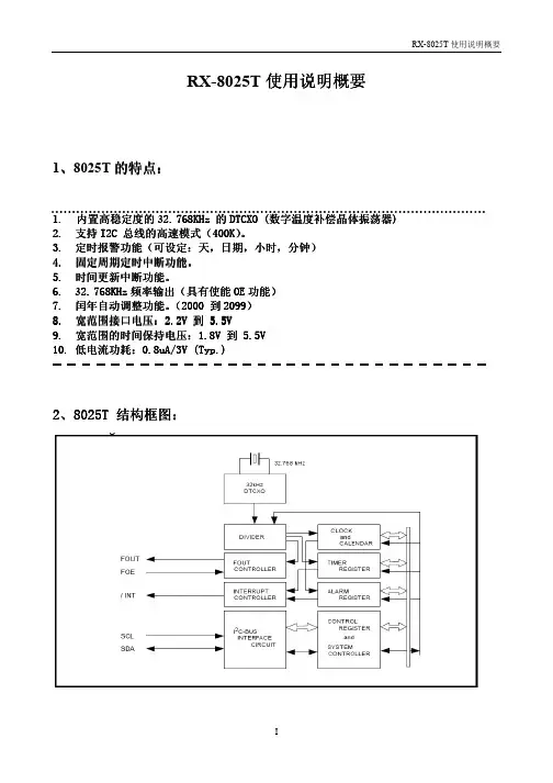
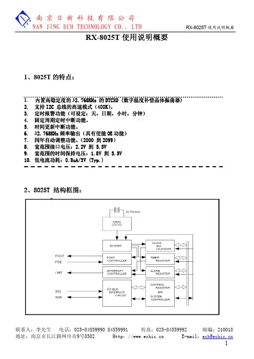
实时时钟芯片RX_8025的原理及其应用
- 格式:pdf
- 大小:612.39 KB
- 文档页数:4


时钟芯片精度比较以前用DS1302 做了万年历,感觉精度不稳定,受晶振和匹配电容的影响,不同的DS1302误差也不一样在网上查资料,精度比较高的两种实时芯片,DS3231,RX8025,两则都能在TB上买到,就是DS3231好贵哦它们的性能呢,就不用多说了,芯片手册里都有,就简单说一下,DS3231-RX8025都是IIC通讯,内置晶振,中断输出,闹钟寄存器。
综上,自己做了一个DS1302-DS3231-RX8025三个一的一个时钟,单片机STC12C5A32S2用来观察它们的精度,经过一周多的时间观察,果然1302不行,做了四个,四个1302变化的都不一样,而3231和8025还是比较理想,4块板子上的3231-8025走时都很准确综合比较DS3231和8025胜出,再综合价格,RX8025为最终胜者。
不过RX8025没有备用电池接口VBAT,需要设计一个主备电切换电路。
LCD是LCD160160,比较少见,在咸鱼上淘的,当初调试这款液晶时,化了很大功夫,大家可以选择自己熟练的液晶显示。
供大家交流学习,有不同看法可以一起交流上传的文件有程序,PCF原理图,以及芯片手册。
这里就贴主函数程序,完整程序见附件1./*****************************************************************************2.1.本程序时测试DS1302,DS3231,RX8025三款时钟芯片的精准度,基于液晶LCD160160显示3.程序说明:4.1.RX8025,DS3231都是IIC通讯,本程序中RX8025采用了比较完善的IIC程序;5.DS3231采用的是比较简单的IIC程序,但两者原理都是一样的。
6.2.本程序中星期的计算是采用公式计算的得来,原型是蔡勒公式,与网上的公式都是7.大同小异。
所以在此程序中的“周”只计算了一次,是根据DS1302读出来的“年月日”数据来8.计算的,因为三个时钟芯片的年月日都一样,所以就只计算一次。
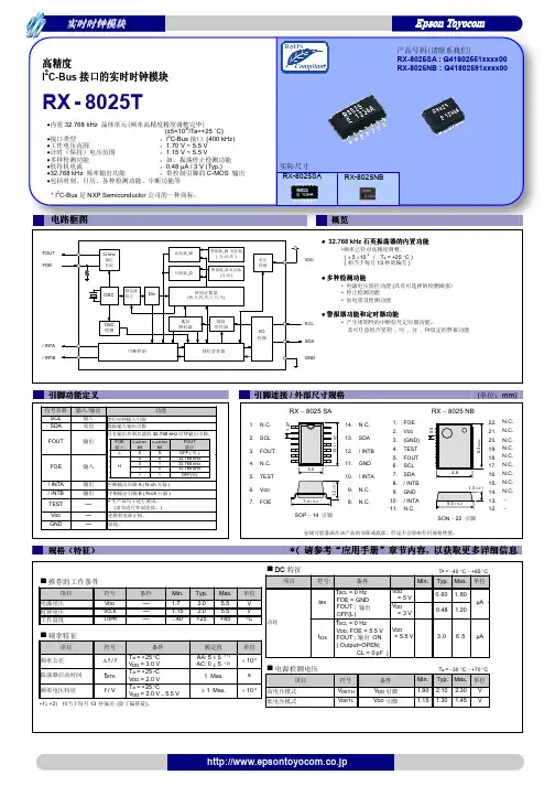
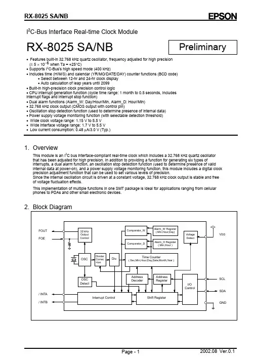
I2C-Bus Interface Real-time Clock ModuleRX-8025 SA/NB Preliminary •Features built-in 32.768 kHz quartz oscillator, frequency adjusted for high precision(± 5 × 10⁻⁶ when Ta = +25°C)• Supports I2C-Bus's high speed mode (400 kHz)• Includes time (H/M/S) and calendar (YR/MO/DATE/DAY) counter functions (BCD code)• Select between 12-hr and 24-hr clock display• Auto calculation of leap years until 2099• Built-in high-precision clock precision control logic• CPU interrupt generation function (cycle time range: 1 month to 0.5 seconds, includesinterrupt flags and interrupt stop function)• Dual alarm functions (Alarm_W: Day/Hour/Min, Alarm_D: Hour/Min)• 32.768 kHz clock output (CMOS output with control pin)• Oscillation stop detection function (used to determine presence of internal data)• Power supply voltage monitoring function (with selectable detection threshold)•Wide clock voltage range: 1.15 V to 5.5 V•Wide interface voltage range: 1.7 V to 5.5 V•Low current consumption: 0.48 µA/3.0 V (Typ.)1. OverviewThis module is an I2C bus interface-compliant real-time clock which includes a 32.768 kHz quartz oscillatorthat has been adjusted for high precision. In addition to providing a function for generating six types ofinterrupts, a dual alarm function, an oscillation stop detection function (used to determine presence of valid internal data at power-on), and a power supply voltage monitoring function, this module includes a digital clock precision adjustment function that can be used to set various levels of precision.Since the internal oscillation circuit is driven at a constant voltage, 32.768 kHz clock output is stable and free of voltage fluctuation effects.This implementation of multiple functions in one SMT package is ideal for applications ranging from cellular phones to PDAs and other small electronic devices.3. Description of Pins3.2. Pin Functions SignalnameI / OFunctionSCL IThis is the serial clock input pin for I 2C communications. Data input and output across the SDA pin is synchronized with this pin's clock signal.Up to 5.5 V can be used for this input, regardless of the power supply voltage.SDA I/OThis pin's signal is used for input and output of address, data, and ACK bits, synchronized with the serial clock used for I 2C communications. The SDA pin is an N-ch open drain pin during output. Be sure to connect a suitable pull-upresistance relative to the signal line capacity.FOUT OThis is the output pin for the 32.768 kHz clock signal with output control provided via theFOE pin.When FOE = High, this pin outputs a 32.768 kHz clock (CMOS output). When FOE = Low or OPEN, clock output is stopped and the signal level is fixed low. FOE I This is an input pin used to control the output mode of the FOUT pin. Pull-down resistance is provided for this pin.When this pin's level is high, a 32.768 kHz is output from the FOUT pin.When this pin's level is low or open, there is no output from the FOUT pin.Up to 5.5 V can be used for this input, regardless of the power supply voltage./INTA OThis interrupt output A pin is an N-ch open drain output.It outputs alarm interrupts (Alarm_D) and periodic interrupts./INTB OThis interrupt output B pin is an N-ch open drain output.It outputs alarm interrupts (Alarm_W).TEST −This pin is used by the manufacturer for testing.Be sure to connect this pin to V DD .V DD −This pin is connected to a positive power supply.GND −This pin is connected to a grounding terminal.N.C. − This pin is not connected to the internal IC.However, note with caution that the RX-8025NB's N.C. pins (pins 14 to 22) are interconnected via the internal frame.Leave N.C. pins open or connect them to GND or V DD .Note: Be sure to connect a bypass capacitor rated at least 0.1 µF between V DD and GND.4. Absolute Maximum RatingsGND = 0 VItem Symbol ConditionRating UnitSupply voltage V DD Between V DD and GND −0.3 to +6.5V Input voltage V I SCL, SDA, FOE pins GND −0.3 to +6.5 V V O1 SDA, /INTA, /INTB pins GND −0.3 to +6.5V Output voltage V O2 FOUT pin GND −0.5 to V DD +0.3 V Storage temperatureT STGWhen stored separately, withoutpackaging−55 to +125 °C5. Operating ConditionsGND = 0 VItem Symbol Condition Min. Typ. Max. UnitPower voltageV DD − 1.73.0 5.5 V Clock voltageV CLK −1.15 3.0 5.5 V Operating temperature T OPR No condensation −40+25 +85 °C Applied voltage when OFFV PUP SCL, SDA, /INTA, /INTB pins −0.35.5 °C6. Frequency CharacteristicsGND=0 VItem Symbol ConditionRatingUnitFrequency tolerance∆ f / fTa = +25°CV DD = 3.0 V Rank AA : 5 ± 5 (∗1)× 10−6 Frequency voltagecharacteristics f / VTa = +25°C V DD = 2 V to 5 V ± 2 Max. × 10−6 / V Frequency temperature characteristics TopTa = −10°C to +70°C,V DD = 3.0 V; +25 °C reference+10 / −120 × 10−6 Oscillation start up time t STATa = +25 °CV DD = 3 V 3 Max. s Aging faTa = +25 °CV DD =3.0 V; first year ± 5 Max.× 10−6 / year∗1)Precision gap per month: 30 seconds (excluding offset value)7. Electrical Characteristics7.1. DC Electrical Characteristics7.1.1. DC electrical characteristics (1)* Unless otherwise specified, GND = 0 V, V DD = 3 V, Ta = −40 °C to +85 °CItem SymbolConditionMin. Typ. Max. UnitCurrentconsumption (1) I DD1 VDD=5 VT.B.D. T.B.D.Currentconsumption (2) I DD2 f SCL = 0Hz, FOE = GND/INTA, /INTB = V DD FOUT;output OFF (low when OFF) VDD=3 V 0.48 1.20 µACurrentconsumption (3) I DD3 VDD=5 V T.B.D. T.B.D.Currentconsumption (4) I DD4 f SCL = 0Hz/INTA, /INTB, FOE = V DD FOUT;32.768 kHz output ON, CL= 0 pF VDD=3 V T.B.D. T.B.D. µACurrentconsumption (5) I DD5 VDD=5 V T.B.D. T.B.D.Currentconsumption (6) I DD6 f SCL = 0Hz/INTA, /INTB, FOE = V DD FOUT;32.768 kHz output ON, CL= 30 pF VDD=3 VT.B.D. T.B.D.µAHigh-level input voltage V IH0.8 × V DD5.5 V Low-level input voltage V IL SCL, SDA, FOE pinsGND − 0.30.2 × V DD V High-level input current I OH FOUT pin, V OH = V DD − 0.5 V−0.5mAI OL1 FOUT pin, V OL = 0.4 V0.5 mA I OL2 /INTA and /INTB pins, V OL = 0.4 V 1.0 mA Low-level input current I OL3 SDA pin, V OL = 0.4 V4.0 mA Input leakage current I ILSCL pin, V I = 5.5 V or GND, V DD = 5.5 V−11 µA7.1.2. DC electrical characteristics (2) * Unless otherwise specified, GND = 0 V, V DD = 3 V, Ta = −40 °C to +85 °CItem Symbol Condition Min. Typ. Max. UnitInput current with pull-down resistanceI FOE FOE pin, V I = 5.5 V0.3 1.0 µA Output current when OFFI OZSDA, /INTA, and /INTB pinsV O = 5.5 V or GND, V DD = 5.5 V−11 µAHigh-voltage mode V DETH V DD pin, Ta = −30 to +70 °C 1.90 2.10 2.30 V Powersupplydetection voltage Low-voltage mode V DETL V DD pin, Ta = −30 to +70 °C1.15 1.30 1.45 V7.2. AC Electrical Characteristics∗ Unless otherwise specified: GND = 0 V, V DD = 1.7 V to 5.5 V, Ta = −40 °C to +85 °C∗ Input conditions: V IH = 0.8 × V DD , V IL = 0.2 × V DD , V OH = 0.8 × V DD , V OL = 0.2 ×V DD , CL = 50 pF Item Symbol Condition Min. Typ. Max. UnitSCL clock frequency f SCL 400 kHzSTART condition set-up time t SU;STA 0.6 µs START condition hold timet HD;STA 0.6 µs Data set-up time t SU;DAT 200 ns Data hold timet HD;DAT 0 ns STOP condition setup timet SU;STO 0.6 µs Bus idle time between a START andSTOP condition t BUF 1.3 µsWhen SCL = "L" t LOW 1.3 µs When SCL = "H"t HIGH 0.6 µs Rise time for SCL and SDA t r 0.3 µs Fall time for SCL and SDA t f 0.3 µs Allowable spike time on bust SP50 nsCaution: When accessing this device, all communication from transmitting a START condition to transmitting a STOPcondition after access should be completed within 0.5 seconds.If such communication requires 0.5 to 1.0 second or longer, the I 2C bus interface is reset by the internal bus timeout function.8. Functional descriptions8.1. Overview of Functions1) Clock functionsThese functions enable setting, timing, and display of data including the year (last two digits), month, date, day, hour, minute, and second. Any (two-digit) year that is a multiple of 4 is treated as a leap year and calculated automatically as such until the year 2099.∗ For details, see "8.2. Description of Registers".2) Clock precision adjustment functionThe clock precision can be adjusted forward or back in units of ± 3.05 × 10⁻⁶. This function can be used to implementa higher-precision clock function, such as by:• Enabling higher clock precision throughout the year by taking seasonal clock precision adjustments into account in advance, or• Enabling correction of temperature-related clock precision variation in systems that include a temperaturedetection function.Note: Only the clock precision can be adjusted. The adjustments have no effect on the 32.768 kHz output from the FOUT pin.∗ For details, see "8.3. Clock Precision Adjustment Function".3) Periodic interrupt functionIn addition to the alarm function, Periodic interrupts can be output via the /INTA pin.Select among five Periodic frequency settings: 2 Hz, 1Hz, 1/60 Hz, hourly, or monthly.Select among two output waveforms for periodic interrupts: an ordinary pulse waveform (2 Hz or 1 Hz) or a waveform (every second, minute, hour, or month) for CPU-level interrupts that can support CPU interrupts.A polling function is also provided to enable monitoring of pin states via registers.∗ For details, see "8.4. Periodic Interrupt Function".4) Alarm functionsThis module is equipped with two alarm functions (Alarm W and Alarm D) that output interrupt signals to the host at preset times. The Alarm W function can be used for day, hour, and minute-based alarm settings, and it outputsinterrupt signals via the /INTB pin. Multiple day settings can be selected (such as Monday, Wednesday, Friday,Saturday, and Sunday). The Alarm D function can be used only for hour or minute-based settings, and it outputs interrupt signals via the /INTA pin.A polling function is also provided to enable checking of each alarm mode by the host.∗ For details on the Alarm W function, see "8.5. Alarm W function" and for the Alarm D function, see "8.6. Alarm D Function".5) Oscillation stop detection function, power drop detection function (voltage monitoring function), and power-on reset detection functionThe oscillation stop detection function uses registers to record when oscillation has stopped.The power drop detection function (supply voltage monitoring function) uses registers to record when the supply voltage drops below a specified voltage threshold value. Use registers to specify either of two voltage thresholdvalues: 2.1 V or 1.3 V. Voltage sampling is performed once per second in consideration of the module's low current consumption.While the oscillation stop detection function is useful for determining when clock data has become invalid, the supply voltage monitoring function is useful for determining whether or not the clock data is able to become invalid. The supply voltage monitoring function can also be used to monitor a battery's supply voltage.When these functions are utilized in combination with the power-on reset detection function, they are useful fordetermining whether clock data is valid or invalid when checking for power-on from 0 V or for back-up.∗ For details, see "8.7. Detection Functions".6) Interface with CPUData is read and written via the I2C bus interface using two signal lines: SCL (clock) and SDA (data).Since neither SCL nor SDA includes a protective diode on the V DD side, a data interface between hosts with differing supply voltages can still be implemented by adding pull-up resistors to the circuit board.The SCL's maximum clock frequency is 400 kHz (when V DD ≥1.7 V), which supports the I2C bus's high-speed mode.∗ For further description of data read/write operations, see "8.8. Reading/Writing Data via the I2C Bus Interface".7) 32.768 kHz clock outputThe 32.768 kHz clock (with precision equal to that of the built-in quartz oscillator) can be output via the FOUT pin.The FOUT pin is a CMOS pin which can be set for clock output when the FOE pin is at high level and for low-level output when the FOE pin is at low level or is left open.Note: The precision of this 32.768 kHz clock output via the FOUT pin cannot be adjusted (even when using the clock precision adjustment function).8.2. Description of Registers8.2.1. Register tableAddress Function bit 7 bit 6 bit 5 bit 4 bit 3 bit 2 bit 1 bit 0∗50 Seconds {S40 S20 S10 S8 S4 S2 S11 Minutes {M40 M20 M10 M8 M4 M2 M12 Hours {{H20P, /AH10 H8 H4 H2 H13 Days {{{{{W4 W2 W14 Days {{D20 D10 D8 D4 D2 D1∗45 Months 0 {{MO10 MO8 MO4 MO2 MO16 Years Y80 Y40 Y20 Y10 Y8 Y4 Y2 Y1∗47 Digital Offset 0 F6 F5 F4 F3 F2 F1 F08 Alarm_W ; Minute {WM40 WM20 WM10 WM8 WM4 WM2 WM19 Alarm_W ; Hour {{WH20WP, /AWH10 WH8 WH4 WH2 WH1A Alarm_W ; Day {WW6 WW5 WW4 WW3 WW2 WW1 WW0B Alarm_D ; Minute {DM40 DM20 DM10 DM8 DM4 DM2 DM1C Alarm_D ; Hour {{DH20DP, /ADH10 DH8 DH4 DH2 DH1∗3∗3D Reserved Reserved∗1∗6∗2E Control 1 WALE DALE /12 , 24 •TEST CT2 CT1 CT0∗1∗1∗6F Control 2 VDSL VDET /XST PON •CTFG WAFG DAFGCaution points:∗1. The PON bit is a power-on reset flag bit.The PON bit is set to "1" when a reset occurs, such as during the initial power-up or when recovering from asupply voltage drop. At the same time, all bits in the Control 1 and Control 2 registers except for the PON and / XST bits are reset to "0".Note: At this point, all other register values are undefined, so be sure to perform a reset before using the module.Also, be sure to avoid entering incorrect date and time data, as clock operations are not guaranteed whenthe time data is incorrect.∗2. The TEST bit is used by the manufacturer for testing. Be sure to set "0" for this bit.∗3. Address D (a reserved register) is used for the manufacturer's settings. Do not read from or write to this register.∗4. All bits marked with a "0" in the above table should be set as "0". Their value when read will be "0".∗5. All bits marked with "{" are read-only bits. Their value when read is always "0".∗6. Bits marked with "•" are RAM bits that can contain any value and are read/write-accessible.However, these bits are cleared to zero when the PON bit value is "1".Address Function bit 7 bit 6 bit 5 bit 4 bit 3 bit 2 bit 1 bit 0E Control 1 WALE DALE /12 , 24 •TEST CT2 CT1 CT0(Default) (0) (0) (0) (0) (0) (0) (0) (0) ∗) The default value is the value that is read (or is set internally) after the PON bit has been set to "1," such as after powering up from 0 V or recovering from a supply voltage drop.1) WALE bitThis bit is used to set up the Alarm W function (to generate alarms matching day, hour, or minute settings).WALE Data Description0 Alarm_W, match comparison operation invalid ∗ DefaultWrite / Read1 Alarm_W, match comparison operation valid (/INTB = "L" when match occurs)∗ For details, see "8.5. Alarm W Function".2) DALE bitThis bit is used to set up the Alarm D function (to generate alarms matching hour or minute settings).DALE Data Description0 Alarm_D, match comparison operation invalid ∗ DefaultWrite / Read1 Alarm_D, match comparison operation valid (/INTA = "L" when match occurs)∗ For details, see "8.6. Alarm D Function".3) /12,24 bitThis bit is used to select between 12-hour clock operation and 24-hour clock operation./12,24 Data Description0 12-hourclock ∗ Default Write / Read1 24-hourclock∗ Be sure to select between 12-hour and 24-hour clock operation before writing the time data.∗ See also "3) Hour counter" in section 8.2.4.4) ’•’ bitThis is a read/write-accessible RAM bit that contains any (arbitrary) data.However, this bit is cleared to zero when the PON bit value is "1".5) TEST bitThis bit is used by the manufacturer for testing. Be sure to write "0" to this bit.Be careful to avoid writing a "1" to this bit when writing to other bits.TEST Data Description0 Normal operation mode ∗ DefaultWrite / Read1 Setting prohibited (manufacturer's test mode)6) CT2, CT1, and CT0 bitsThese bits are used to set up the operation of the periodic interrupt function that uses the /INTA pin./INTA pin's output settingCT2 CT1 CT0Waveform mode Cycle/Fall timing0 0 0 −/INTA = Hi-Z (= OFF) ∗ Default0 0 1 −/INTA = Fixed low0 1 0 Pulse mode ∗1) 2 Hz (50% duty)0 1 1 Pulse mode ∗1) 1 Hz (50% duty)1 0 0 Level mode ∗2)Once per second (Synchronous with per-second count-up)1 0 1 Level mode ∗2)Once per minute (Occurs when seconds reach ":00")1 1 0 Level mode ∗2)Once per hour (Occurs when minutes and seconds reach "00:00")1 1 1 Level mode ∗2)Once per month (Occurs at 00:00:00 on first day of month)∗ For details, see "8.4. Periodic Interrupt".Address Function bit 7 bit 6 bit 5 bit 4 bit 3 bit 2 bit 1 bit 0F Control 2 VDSL VDET / XST PON •CTFG WAFG DAFG(Default) (0) (0) (−) (1) (0) (0) (0) (0) ∗1) The default value is the value that is read (or is set internally) after the PON bit has been set to "1," such as after powering up from 0 V or recovering from a supply voltage drop.∗2) '"−" indicates undefined status.1) VDSL bitThis bit is used to set the power drop detection function's threshold voltage value.VDSL Data Description0 Sets 2.1 V as the power drop detection function's thresholdvoltage value ∗ DefaultWrite / Read1 Sets 1.3 V as the power drop detection function's threshold voltage value∗ For details, see "8.7. Detection Functions".2) VDET bitThis bit indicates the power drop detection function's detection results.VDET = "1" once a power voltage drop has occurred.VDET Data Description0 Clears the VDET bit to zero, restarts the power drop detectionoperation and sets up for next power drop detection operation∗ DefaultWrite1 Setting prohibited (do not set this bit value, even though it has no effect)0 Power drop was not detected∗ DefaultRead1 Power drop was detected(result is that bit value is held until cleared to zero)∗ For details, see "8.7. Detection Functions".3) /XST bitThis bit indicates the oscillation stop detection function's detection results.If a "1" has already been written to this bit, it is cleared to zero when stopping of internal oscillation is detected./ XST Data Description0 Setting prohibited (do not set this bit value, even though it has no effect)Write1 Sets the oscillation stop detection function as use-enabled and sets up for next detection operation0 Oscillation stop was detected(result is that bit value is held until a "1" is written)Read1 Oscillation stop was not detected∗ For details, see "8.7. Detection Functions".4) PON bitThis bit indicates the power-on reset detection function's detection results.The PON bit is set (= 1) when the internal power-on reset function operates.PON Data Description0 Clears the PON bit to zero and sets up next detection operationWrite1 Setting prohibited (do not set this bit value, even though it has no effect)0 Power-on reset was not detectedRead1 Power-on reset was detected(result is that bit value is held until cleared to zero)∗ Default∗ When PON = "1" all bits in the Clock Precision Adjustment register and in the Control 1 and Control 2 registers (except for the PON and / XST bits) are reset to "0". This also causes output from /INTA and /INTB pin to be stopped (= Hi-Z).∗ For details, see "8.7. Detection Functions".5) ' • ' bitBits marked with "•" are RAM bits that can contain any value and are read/write-accessible.However, these bits are cleared to zero when the PON bit value is "1".6) CTFG bitDuring a read operation, this bit indicates the /INTA pin's periodic interrupt output status.This status can be set as OFF by writing a "0" to this bit when /INTA = " L".CTFG Data Description0 A "0" can be written only when the periodic interrupt is in levelmode, at which time the /INTA pin is set to OFF (Hi-z) status.(Only when Alarm_D does not match)∗ After a "0" is written, the value still becomes "1" again at thenext cycle.∗ DefaultWrite1 Setting prohibited (do not set this bit value, even though it has no effect)0 Periodic interrupt output OFF status; /INTA = OFF (Hi-z)∗ Default Read1 Periodic interrupt output ON status; /INTA = "L"∗ For details, see "8.4. Periodic Interrupt Function".7) WAFG bitThis bit is valid only when the WALE bit value is "1".The WAFG bit value becomes "1" when Alarm W has occurred.The /INTB = "L" status that is set at this time can be set to OFF by writing a "0" to this bit.WAFG Data Description0 /INTB pin = OFF (Hi-z) ∗ DefaultWrite1 Setting prohibited (do not set this bit value, even though it has no effect)0 Alarm_W time setting does not match current time(This bit's value is always "0" when the WALE bit's setting is "0")∗ DefaultRead1 Alarm_W setting matches current time(Result is that bit value is held until cleared to zero)∗ For details, see "8.5. Alarm W Function".8) DAFG bitThis bit is valid only when the DALE bit value is "1". The DAFG bit value becomes "1" when Alarm D has occurred.The /INTA = "L" status that is set at this time can be set to OFF by writing a "0" to this bit.DAFG Data Description0 /INTA pin = OFF (Hi-z) (but only when the periodic interruptoutput status is OFF)∗ DefaultWrite1 Setting prohibited (do not set this bit value, even though it has no effect)0 Alarm_D time setting does not match current time(This bit's value is always "0" when the DALE bit's setting is "0")∗ DefaultRead1 Alarm_D time setting matches current time (result is that bit value is held until cleared to zero)∗ For details, see "8.6. Alarm D function".8.2.4. Time counter (Reg 0 to 2)Address Function bit 7 bit 6 bit 5 bit 4 bit 3 bit 2 bit 1 bit 00 Seconds {S40 S20 S10 S8 S4 S2 S11 Minutes {M40 M20 M10 M8 M4 M2 M12 Hours {{H20P, /AH10 H8 H4 H2 H1∗) "□" indicates write-protected bits. A zero is always read from these bits.• The time counter counts seconds, minutes, and hours.• The data format is BCD format(except during 12-hour display mode). For example, when the "seconds" register value is "0101 1001" it indicates 59 seconds.∗ Note with caution that writing non-existent time data may interfere with normal operation of the time counter.1) Second counterAddress Function bit 7 bit 6 bit 5 bit 4 bit 3 bit 2 bit 1 bit 00 Seconds{S40 S20 S10 S8 S4 S2 S1• This second counter counts from "00" to "01," "02," and up to 59 seconds, after which it starts again from00 seconds.• When a value is written to the second counter, the internal counter is also reset to zero in less than one second.2) Minute counterAddress Function bit 7 bit 6 bit 5 bit 4 bit 3 bit 2 bit 1 bit 01 Minutes {M40 M20 M10 M8 M4 M2 M1• This minute counter counts from "00" to "01," "02," and up to 59 minutes, after which it starts again from00 minutes.3) Hour counterAddress Function bit 7 bit 6 bit 5 bit 4 bit 3 bit 2 bit 1 bit 02 Hours {{H20P , /AH10 H8 H4 H2 H1• The hour counter counts hours, and its clock mode differs according to the value of its /12,24 bit. • During 24-hour clock operation, bit 5 functions as H20 (two-digit hour display). During 12-hour clock operation, bit 5 functions as an AM/PM indicator ("0"indicates AM and "1" indicates PM).Address Function bit 7 bit 6 bit 5 bit 4 bit 3 bit 2 bit 1 bit 03 Days {{{{{W4 W2 W1∗) "□" indicates write-protected bits. A zero is always read from these bits.• The day counter is a divide-by-7 counter that counts from 00 to 01 and up 06 before starting again from 01.• The correspondence between days and count values is shown below.Days W4 W2 W1 Day Remark00h0 0 0 Sundayh010 0 1 Mondayh0 1 0 Tuesday02Write / Readh0 1 1 Wednesday031 0 0 Thursday04h1 0 1 Friday 05hh1 1 0 Saturday06prohibit 1 1 1 −Do not enter a setting for this bit.Write8.2.6. Calendar counter (Reg 4 to 6)Address Function bit 7 bit 6 bit 5 bit 4 bit 3 bit 2 bit 1 bit 04 Days {{D20 D10 D8 D4 D2 D15 Months 0 {{MO10 MO8 MO4 MO2 MO16 Years Y80 Y40 Y20 Y10 Y8 Y4 Y2 Y1∗1) Be sure to set a "0" for any bit whose value is shown above as "0". A zero is returned when any of these bits is read.∗2) '"□" indicates write-protected bits. A zero is always read from these bits.• The auto calendar function updates all dates, months, and years from January 1, f2001 to December 31, 2099.• The data format is BCD format. For example, a date register value of "0011 0001" indicates the 31st.∗ Note with caution that writing non-existent date data may interfere with normal operation of the calendar counter.1) Date counterAddress Function bit 7 bit 6 bit 5 bit 4 bit 3 bit 2 bit 1 bit 04 Days {{D20 D10 D8 D4 D2 D1• The updating of dates by the date counter varies according to the month setting.∗ A leap year is set whenever the year value is a multiple of four (such as 04, 08, 12, 88, 92, or 96).Days Month Date update pattern1, 3, 5, 7, 8, 10, or 12 01, 02, 03 to 30, 31, 01…4, 6, 9, or 11 01, 02, 03 to 30, 01, 02…Write / ReadFebruary in leap year 01, 02, 03 to 28, 29, 01…February in normal year 01, 02, 03 to 28, 01, 02…2) Month counterAddress Function bit 7 bit 6 bit 5 bit 4 bit 3 bit 2 bit 1 bit 05 Months 0 {{MO10 MO8 MO4 MO2 MO1• The month counter counts from 01 (January), 02 (February), and up to 12 (December), then starts againat 01 (January).∗ Be sure to set a "0" for any bit whose value is shown above as "0". A zero is returned when any of thesebits is read.3) Year counterAddress Function bit 7 bit 6 bit 5 bit 4 bit 3 bit 2 bit 1 bit 06 Years Y80 Y40 Y20 Y10 Y8 Y4 Y2 Y1• The year counter counts from 00, 01, 02 and up to 99, then starts again at 00.∗ In any year that is a multiple of four (04, 08, 12, 88, 92, 96, etc.), the dates in February are counted from01, 02, 03 and up to 29 before starting again at 01.。
(50条消息)时钟芯片RX8025T的电源设计2017-06-12 14:30:05最后发布:2017-06-12 14:30:05首发:2017-06-12 14:30:05转:/news/4392.htmlEPSON的RX-8025T实时时钟芯片具有极低的功耗,内置高稳定度的32.768KHz的晶振,并自带温度补偿功能,通过相应的设置可以提高时钟精度。
由于其强大的功能以及极简化的外围电路,得到电表厂商的青睐,成为了智能四表领域应用比较广泛的一款时钟芯片。
下面以“时钟在电池供电的情况下工作5年”为目标,结合笔者的项目谈一谈RX-8025T电源的设计经验。
RX-8025T的电源方案一般如图1所示。
时钟芯片供电采用二极管隔离,设计思路为节约时钟电池损耗,采取系统电源优先供电原则。
设计时需要注意如下几点:1)两个二极管的压降不同从RX-8025T芯片的数据手册上我们可以看到,其工作电压范围比较宽:从2.2V到5.5V,这就使得我们可以在系统电源V3P3和电池供电VBAT_RTC(一般为3.6V)上使用具有正向压降的二极管,实际输入到时钟芯片的RTC在3V~3.3V之间。
需要注意的是,电池的二极管V23和系统电源的二极管V20选型必须不一样(如图2所示),这是因为一般的锂电池电压为3.6V,而系统电压为3.3V,同样压降的二极管之后,电池电压依然是偏高的。
这样一来,即使在外部电源供电时,时钟也会消耗电池的电量。
如果系统电压线路上的二极管选用SS14降低0.2V左右,那么时钟电路上的二极管选择管压降较大的LL4148降低0.6V左右则可以很好的解决这个问题。
当外部供电时,系统电源经过LDO转出的3.3V电压在经过SS14后得到大于电池经过LL4148后的电压,此时RX-8025T由主电源供电;外部停电后系统电源无电时,切换到锂电池供电状态。
2)电池电源采用储能电容以防止电压滞后锂电池在业内主流的选择为1200mAh容量的锂亚硫酰氯电池,供电电压为3.66V,自身容量年损耗极小,可以忽略。