tda7293
- 格式:pdf
- 大小:428.38 KB
- 文档页数:16
Value
Unit
±60
V
90
V
90
V
±30
V
90
V
90
V
120
V
120
V
120
V
120
V
120
V
100
V
10
A
50
W
0 to 70
°C
150
°C
THERMAL DATA
Symbol Rth j-case
Description Thermal Resistance Junction-case
2/15
ICLEAK SLAVE FUNCTION pin 4 (Ref: to pin 8 -VS)
VSlave SlaveThreshold VMaster Master Threshold
Test Condition
d = 1%: RL = 4Ω; VS = ± 29V, d = 10% RL = 4Ω ; VS = ±29V PO = 5W; f = 1kHz PO = 0.1 to 50W; f = 20Hz to 15kHz VS ≤ ± 40V
10
MUTE
9
STAND-BY
8
-VS (SIGNAL)
7
+VS (SIGNAL)
6
BOOTSTRAP
5
CLIP AND SHORT CIRCUIT DETECTOR
4
SIGNAL GROUND
3
NON INVERTING INPUT
2
INVERTING INPUT
1
STAND-BY GND
TAB CONNECTED TO PIN 8
Symbol VS Iq Ib VOS IOS PO
Parameter Supply Range Quiescent Current Input Bias Current Input Offset Voltage Input Offset Current RMS Continuous Output Power
Unit V mA µA mV µA W
W
% % A V/µs dB dB µV µV kΩ dB °C °C
V V dB mA
V V dB
% %
µA
V V
3/15
TDA7293
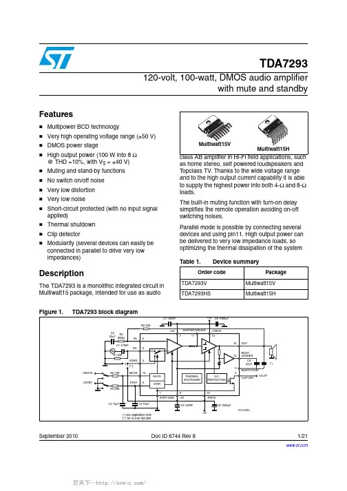
Figure 2: Typical Application P.C. Board and Component Layout (scale 1:1)
VMUTE VSTBY
C7 100nF
+Vs C6 1000µF
R3 22K
C2 22µF
R2 680Ω
IN- 2
C1 470nF IN+ 3
R1 22K
SGND 4 (**)
+Vs +
R5 10K R4 22K C3 10µF
MUTE 10 STBY 9
MUTE STBY
C4 10µF
1 STBY-GND
Figure 1: Typical Application and Test Circuit
MULTIPOWER BCD TECHNOLOGY
Multiwatt15V
Multiwatt15H
ORDERING NUMBERS:
TDA7293V
TDA7293HS
class TV). Thanks to the wide voltage range and to the high out current capability it is able to supply the highest power into both 4Ω and 8Ω loads.
DESCRIPTION
The TDA7293 is a monolithic integrated circuit in Multiwatt15 package, intended for use as audio class AB amplifier in Hi-Fi field applications (Home Stereo, self powered loudspeakers, Top-
Min. ±12 -10 75 90
5 29 100
3.5 70
3.5 60 30
3
Typ.
50 0.3
80 80 100 100 0.005 6.5 10 80 30 1 3
75 150 160
90 0.5
80
10 40
Max. ±50 100
1 10 0.2
0.1
31 10
1.5 1 1.5
50 3 1
COMPONENTS SUGGESTED VALUE
PURPOSE
LARGER THAN SUGGESTED
SMALLER THAN SUGGESTED
R1 (*)
22k
INPUT RESISTANCE INCREASE INPUT DECREASE INPUT
IMPEDANCE
IMPEDANCE
R2 R3 (*)
Typ
Max
Unit
1
1.5
°C/W
TDA7293
ELECTRICAL CHARACTERISTICS (Refer to the Test Circuit VS = ±40V, RL = 8Ω, Rg = 50 Ω; Tamb = 25°C, f = 1 kHz; unless otherwise specified).
ON/OFF TIME
ON/OFF TIME;
POP NOISE
R5
10k
MUTE TIME
LARGER MUTE
d
ISC SR GV GV eN
Ri SVR TS
Total Harmonic Distortion (**)
Current Limiter Threshold Slew Rate Open Loop Voltage Gain Closed Loop Voltage Gain (1) Total Input Noise
®
TDA7293
120V - 100W DMOS AUDIO AMPLIFIER WITH MUTE/ST-BY
VERY HIGH OPERATING VOLTAGE RANGE (±50V) DMOS POWER STAGE HIGH OUTPUT POWER (100W @ THD = 10%, RL = 8Ω, VS = ±40V) MUTING/STAND-BY FUNCTIONS NO SWITCH ON/OFF NOISE VERY LOW DISTORTION VERY LOW NOISE SHORT CIRCUIT PROTECTED (WITH NO INPUT SIGNAL APPLIED) THERMAL SHUTDOWN CLIP DETECTOR MODULARITY (MORE DEVICES CAN BE EASILY CONNECTED IN PARALLEL TO DRIVE VERY LOW IMPEDANCES)
The built in muting function with turn on delay simplifies the remote operation avoiding switching on-off noises. Parallel mode is made possible by connecting more device through of pin11. High output power can be delivered to very low impedance loads, so optimizing the thermal dissipation of the system.
680Ω 22k
CLOSED LOOP GAIN DECREASE OF GAIN INCREASE OF GAIN SET TO 30dB (**) INCREASE OF GAIN DECREASE OF GAIN
R4
22k
ST-BY TIME
LARGER ST-BY
SMALLER ST-BY
CONSTANT
4/15
TDA7293
APPLICATION SUGGESTIONS (see Test and Application Circuits of the Fig. 1)
The recommended values of the external components are those shown on the application circuit of Figure 1. Different values can be used; the following table can help the designer.
A = curve f = 20Hz to 20kHz f = 100Hz; Vripple = 0.5Vrms DEVICE MUTED DEVICE SHUT DOWN
THD = 1% ; RL = 10KΩ to 5V THD = 10% ; RL = 10KΩ to 5V PO = 50W
Note (1): GVmin ≥ 26dB
Input Resistance Supply Voltage Rejection Thermal Protection
STAND-BY FUNCTION (Ref: to pin 1) VST on Stand-by on Threshold VST off Stand-by off Threshold ATTst-by Stand-by Attenuation Iq st-by Quiescent Current @ Stand-by MUTE FUNCTION (Ref: to pin 1) VMon Mute on Threshold VMoff Mute off Threshold ATTmute Mute AttenuatIon CLIP DETECTOR Duty Duty Cycle ( pin 5)