
HF12FF(JQC-12FF)_cn
- 格式:pdf
- 大小:122.02 KB
- 文档页数:3
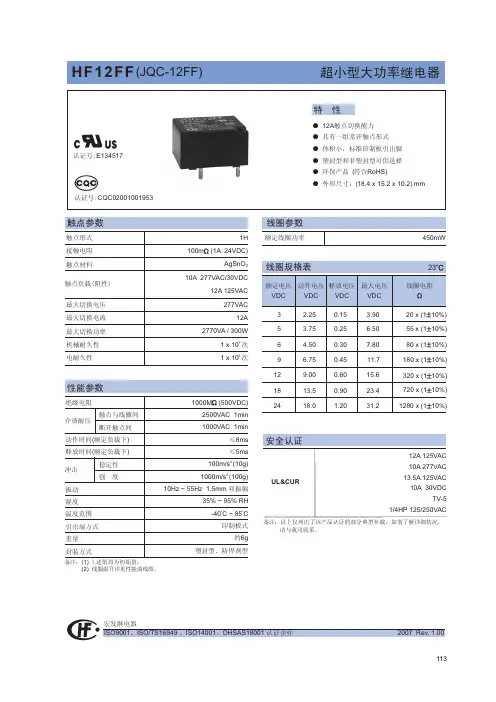


产 品 型 号JQC-3FF JQC-7FD JQC-21FF HM420产 品 照 片外 形 尺 寸19 x 15.5 x 15.5 22.5 x 16.5 x 16.5 20.1 x 16.5 x 20.2 19 x 15.5 x 15.5主 要 特 点 z 一组动合或一组转换触点; z 触点与线圈耐压1500V ; z 塑封或非塑封形式; z 环境温度可达70°C ; z 触电电流可达15A 。
z 一组动合或一组转换触点;z 触点与线圈耐压2000V ; z 塑封或非塑封形式; z 环境温度可达85°C ; z 触电电流可达12A 。
z 一组动合或一组转换触点; z 触点与线圈耐压1500V ; z 塑封或非塑封形式;z 环境温度可达70°C ;z 触电电流可达15A 。
z 二组转换触点; z 标准型和灵敏型z 触点与线圈耐压1500V ;z 塑封或非塑封形式; z 环境温度可达80°C 。
触 点 参 数触 点 形 式 1H (1A )或1Z (1C ) 1H (1A )或1Z (1C ) 1H (1A )或1Z (1C )2Z 材 料 银合金 银合金 银合金 银合金最大切换电流10A 12A 15A 5A 最大切换电压 277V AC ;30VDC 277V AC ;28VDC 277V AC ;30VDC 277V AC ;28VDC最大切换功率2770V A / 240W 2770V A / 280W 2500V A / 280W 575V A / 130W 额 定 负 载 (阻性)1H :10A 277V AC15A 120V ACTV-5 120V AC 1Z :10A 277V AC 1H :10A 250V AC / 28VDC 1Z :12A 125V AC 7A 250V AC / 28VDC 1H :15A 120V AC 24VDC 1Z :10A 120V AC 6A 240V AC / 24VDC1B :灯载1000W 120V ACA :2A 26VDC / 115V AC C :5A 26VDC / 115V AC 线 圈 参 数额 定 电 压 3~48VDC 3~48VDC 3~48VDC 标准型:3~115VDC灵敏型:3~48VDC功 耗 0.36W 0.36W 0.36W ,0.53W (48VDC ) 标准型:0.64W~0.93W灵敏型:0.18W性 能 参 数绝 缘 电 阻 100M Ω(500VDC) 100M Ω(500VDC) 100M Ω(500VDC) 10000M Ω(100VDC) 介 质 耐 压 (线圈与触点间) 1500Vrms 1min2000Vrms 1min1500Vrms 1min1500Vrms 1min 环 境 温 度 -40°C~70°C -40°C~85°C -40°C~70°C 标准型:-55°C~80°C 灵敏型:-55°C~95°C动作时间/释放时间 10ms / 5ms10ms / 5ms10ms / 5ms16ms / 4ms机械寿命(min ) 1x10⁷ 1x10⁷ 1x10⁷ 1x10⁷ 电气寿命(min ) 1x10⁵ 1x10⁵ 1x10⁵ 1x10⁵安 装 孔 位 图引 出 端 方 式 PCB PCB PCB PCB 、插入/焊接式安 全 认 证UL&CUR TUV CQC UL&CUR CQC UL&CUR TUV CQC UL&CUR 安 规 认 证 号 E170653、R50033761 CQC 03001002865 E170653 CQC 03001007462 E170653、R50033761 CQC 03001002865E43203 对 照 型 号 OMRON :G5L SONGCHUAN :833H NAIS :JS P&B :T72FUJITSU :FBR161-HZETTLER :AZ943OMRON :G5L SONGCHUAN :812BH NAIS :JS TYCQ :V23001 OEG :SRUDH OMRON :G5L SONGCHUAN :81H FUJITSU :FBR100 OEG :SRUDH OMRON :MHS AROMAT :K P&B :R10 ZETTLER :AZ420 详细资料页码01-02 03-05 06-07 08-10产 品 型 号HM421 HM431 HM805HM807产 品 照 片外 形 尺 寸30 x 18.7 x 3036 x 18.7 x 3053.9 x 48 x60.384.5 x 63.5 x 61(长底座) 63.5 x 63.5 x 61(长底座)主 要 特 点z 四组转换触点; z 标准型和灵敏型;z 触点与线圈耐压1500V ; z 塑封或非塑封形式; z 环境温度可达80°C 。
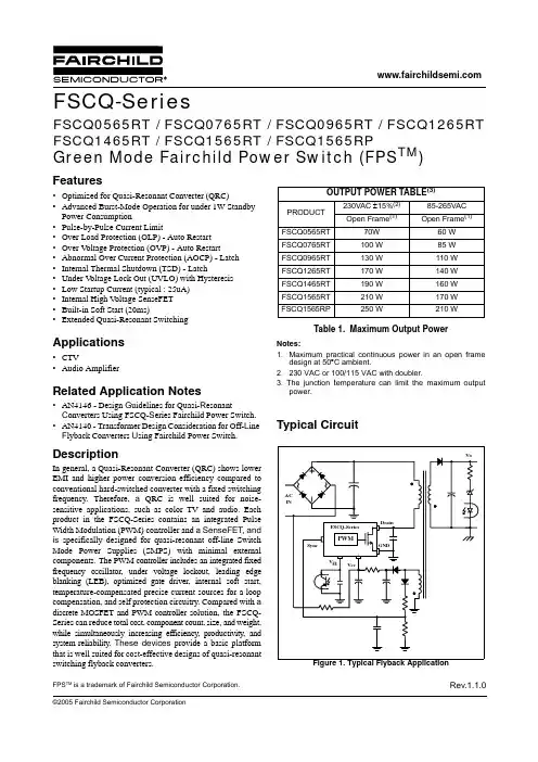
©2005 Fairchild Semiconductor CorporationRev.1.1.0FPS TM is a trademark of Fairchild Semiconductor Corporation.Features•Optimized for Quasi-Resonant Converter (QRC)•Advanced Burst-Mode Operation for under 1W Standby Power Consumption•Pulse-by-Pulse Current Limit•Over Load Protection (OLP) - Auto Restart •Over V oltage Protection (OVP) - Auto Restart•Abnormal Over Current Protection (AOCP) - Latch •Internal Thermal Shutdown (TSD) - Latch•Under V oltage Lock Out (UVLO) with Hysteresis •Low Startup Current (typical : 25uA)•Internal High V oltage SenseFET •Built-in Soft Start (20ms)•Extended Quasi-Resonant SwitchingApplications•CTV•Audio AmplifierRelated Application Notes•AN4146 - Design G uidelines for Quasi-R esonantC onverters Using FSCQ-S eries Fairchild Power Switch .•AN4140 - Transformer Design Consideration for Off-L ine F lyback Converters U sing Fairchild Power Switch.DescriptionIn general, a Quasi-Resonant Converter (QRC) shows lower EMI and higher power conversion efficiency compared to conventional hard-switched converter with a fixed switching frequency. Therefore, a QRC is well suited for noise-sensitive applications, such as color TV and audio. Each product in the FSCQ-Series contains an integrated Pulse Width Modulation (PWM) controller and a SenseFET, and is specifically designed for quasi-resonant off-line Switch Mode Power Supplies (SMPS) with minimal external components. The PWM controller includes an integrated fixed frequency oscillator, under voltage lockout, leading edge blanking (LEB), optimized gate driver, internal soft start,temperature-compensated precise current sources for a loop compensation , and self protection circuitry. Compared with a discrete MOSFET and PWM controller solution, the FSCQ-Series can reduce total cost, component count, size , and weight,while simultaneously increasing efficiency, productivity, and system reliability. These devices provide a basic platform that is well suited for cost-effective designs of quasi-resonant switching flyback converters.Table 1. Maximum Output PowerNotes:1. Maximum practical continuous power in an open framedesign at 50°C ambient.2. 230 VAC or 100/115 VAC with doubler.3. The junction t emperature can limit the maximum outputpower.Typical CircuitOUTPUT POWER TABLE (3)PRODUCT 230VAC ±15%(2)85-265VAC Open Frame (1)Open Frame (1)FSCQ0565RT 70W 60 W FSCQ0765RT 100 W 85 W FSCQ0965RT 130 W 110 W FSCQ1265RT 170 W 140 W FSCQ1465RT 190 W 160 W FSCQ1565RT 210 W 170 W FSCQ1565RP250 W210 WFSCQ-SeriesFSCQ0565RT / FSCQ0765RT / FSCQ0965RT / FSCQ1265RT FSCQ1465RT / FSCQ1565RT / FSCQ1565RPGreen Mode Fairchild Power Switch (FPS TM )FSCQ-SERIESInternal Block DiagramFigure 2.Functional Block Diagram of FSCQ-Series 2FSCQ-SERIES3Pin DefinitionsPin ConfigurationFigure 3.Pin Configuration (Top View)Pin NumberPin Name Pin Function Description1Drain High voltage power SenseFET drain connection. 2GND This pin is the control ground and the SenseFET source.3VccThis pin is the positive supply input. This pin provides internal operating current for both start-up and steady-state operation.4VfbThis pin is internally connected to the inverting input of the PWM comparator.The collector of an opto-coupler is typically tied to this pin. For stable operation, a capacitor should be placed between this pin and GND. If the voltage of this pin reaches 7.5V, the over load protection triggers , which results in the FPS shutting down.5SyncThis pin is internally connected to the sync detect comparator for quasi-resonant switching. In normal quasi-resonant operation, the threshold of the sync comparator is 4.6V/2.6V. Whereas, the sync threshold is changed to3.0V/1.8V in an extended quasi-resonant operation.FSCQ-SERIES4Absolute Maximum Ratings(Ta=25°C, unless otherwise specified)Parameter Symbol Value Unit Drain Pin Voltage V DS 650V Supply VoltageV CC 20V Analog Input Voltage RangeV sync -0.3 to 13V V V FB-0.3 to V CCVDrain Current Pulsed (1)I DMFSCQ0565RT 11.2AFSCQ0765RT 15.2FSCQ0965RT16.4FSCQ1265RT 21.2FSCQ1465RT 22FSCQ1565RT 26.4FSCQ1565RP 33.2Continuous Drain Current(Tc=25°C) (Tc : Case Back Surface Temperature)I DFSCQ0565RT 2.8 A (rms)FSCQ0765RT3.8FSCQ0965RT4.1FSCQ1265RT5.3FSCQ1465RT 5.5FSCQ1565RT6.6FSCQ1565RP 8.3Continuous Drain Current * (T DL =25°C)(T DL :Drain Lead Temperature)I D *FSCQ0565RT 5 A (rms)FSCQ0765RT 7FSCQ0965RT7.6FSCQ1265RT 11FSCQ1465RT 12FSCQ1565RT 13.3FSCQ1565RP 15Continuous Drain Current (T C =100°C)I DFSCQ0565RT 1.7 A (rms)FSCQ0765RT 2.4FSCQ0965RT2.6FSCQ1265RT3.4FSCQ1465RT 3.5FSCQ1565RT4.4FSCQ1565RP5.5Single-Pulsed Avalanche Energy (2)E ASFSCQ0565RT 400mJFSCQ0765RT 570FSCQ0965RT630FSCQ1265RT 950FSCQ1465RT 1000FSCQ1565RT 1050FSCQ1565RP1050FSCQ-SERIES5Notes:1. Repetitive rating: Pulse width limited by maximum junction temperature2. L = 15mH, starting T j = 25°C, These parameters, although guaranteed at the design, are not tested in mass production.Thermal Impedance(Ta=25°C unless otherwise specified)Total Power Dissipation(Tc=25°C with Infinite Heat Sink)P DFSCQ0565RT 38WFSCQ0765RT45FSCQ0965RT49FSCQ1265RT 50FSCQ1465RT 60FSCQ1565RT 75FSCQ1565RP98Operating Junction Temperature T J +150°C Operating Ambient Temperature T A -25 to +85°C Storage Temperature Range T STG-55 to +150°C ESD Capability, HBM Model (All pins except Vfb)- 2.0(GND-Vfb=1.7kV)kV ESD Capability, Machine Model (All pins except Vfb)-300(GND-Vfb=170V)V ParameterSymbolValue UnitJunction to Case Thermal ImpedanceθJCFSCQ0565RT 3.29°C/WFSCQ0765RT 2.60FSCQ0965RT2.55FSCQ1265RT 2.50FSCQ1465RT 2.10FSCQ1565RT 2.00FSCQ1565RP1.28FSCQ-SERIES6Electrical Characteristics (SenseFET Part)(Ta=25°C unless otherwise specified)ParameterSymbol Condition Min.Typ.Max.Unit Drain-Source Breakdown Voltage BV DSS V GS = 0V, I D = 250μA 650--V Zero Gate Voltage Drain CurrentI DSSV DS = 650V,V GS = 0V --250μADrain-Source ON-State ResistanceR DS(ON)FSCQ0565RT V GS = 10V, I D = 1A - 1.76 2.2ΩFSCQ0765RTV GS = 10V, I D = 1A - 1.4 1.6ΩFSCQ0965RTV GS = 10V, I D = 1A - 1.0 1.2ΩFSCQ1265RT V GS = 10V, I D = 1A-0.750.9ΩFSCQ1465RT V GS = 10V, I D = 1A -0.70.8ΩFSCQ1565RTV GS = 10V, I D = 1A-0.530.7ΩFSCQ1565RP V GS = 10V, I D = 1A -0.530.7ΩInput Capacitance C ISSFSCQ0565RT V GS = 0V, V DS = 25V, f = 1MHz-1080-pFFSCQ0765RT -1415-FSCQ0965RT-1750-FSCQ1265RT -2400-FSCQ1465RT -2400-FSCQ1565RT -3050-FSCQ1565RP -3050-Output Capacitance C OSSFSCQ0565RT V GS = 0V, V DS = 25V,f = 1MHz-90-pFFSCQ0765RT -100-FSCQ0965RT-130-FSCQ1265RT-175-FSCQ1465RT -185-FSCQ1565RT -220-FSCQ1565RP-220-FSCQ-SERIES7Electrical Characteristics (Continued)(Ta=25°C unless otherwise specified)Note:1. These parameters, although guaranteed, are tested only in EDS (wafer test) process.2. These parameters, although guaranteed at the design, are not tested in mass production.ParameterSymbolConditionMin.Typ.Max.UnitCONTROL SECTION Switching FrequencyF OSC V FB = 5V, V CC = 18V 182022kHz Switching Frequency Variation (1)ΔF OSC -25°C ≤ Ta ≤ 85°C 0±5±10%Feedback Source Current I FB V FB = 0.8V, V CC = 18V 0.50.650.8mA Maximum Duty Cycle D MAX V FB = 5V, V CC = 18V 929598%Minimum Duty Cycle D MIN V FB = 0V, V CC = 18V -0-%UVLO Threshold Voltage V START V FB =1V 141516V V STOP V FB =1V8910V Soft Start Time (1)T SS-182022msBURST MODE SECTIONBurst Mode Enable Feedback Voltage V BEN -0.250.400.55V Burst Mode Feedback Source Current I BFB V FB = 0V60100140uA Burst Mode Switching Time T BS V FB = 0.9V, Duty =50% 1.2 1.4 1.6ms Burst Mode Hold Time T BHV FB = 0.9V -> 0V1.21.41.6msPROTECTION SECTION Shutdown Feedback Voltage V SD V CC = 18V7.07.58.0V Shutdown Delay Current I DELAY V FB = 5V, V CC = 18V 456μA Over Voltage Protection V OVP V FB = 3V 111213V Over Current Latch Voltage (1)V OCL V CC = 18V0.9 1.0 1.1V Thermal Shutdown Temp (2)T SD-140--°CFSCQ-SERIES8Electrical Characteristics (Continued)(Ta=25°C unless otherwise specified)Note:1. This parameter is the current flowing in the control IC.2. These parameters indicate inductor current.3. These parameters, although guaranteed, are tested only in EDS (wafer test) process.Parameter Symbol Condition Min.Typ.Max.Unit Sync SECTIONSync Threshold in Normal QR (H)V SH1V CC = 18V, V FB = 5V4.2 4.65.0V Sync Threshold in Normal QR (L)V SL1 2.3 2.6 2.9V Sync Threshold in Extended QR (H)V SH2 2.7 3.0 3.3V Sync Threshold in Extended QR (L)V SL2 1.6 1.8 2.0V Extended QR Enable Frequency F SYH -90-kHz Extended QR Disable Frequency F SYL-45-kHzTOTAL DEVICE SECTION Operating Supply Current (1)- In Normal Operation I OPFSCQ0565RT V FB = 5V-46mAFSCQ0765RT -46FSCQ0965RT-68FSCQ1265RT -68FSCQ1465RT -79FSCQ1565RT -79FSCQ1565RP-79- In Burst Mode (Non-switching)I OB V FB = GND -0.250.50mA Startup Current I START V CC = V START -0.1V -2550uA Sustain Latch Current (3)I SNV CC = V STOP -0.1V-50100uA CURRENT SENSE SECTIONMaximum Current Limit (2)I LIMFSCQ0565RT V CC = 18V, V FB = 5V3.08 3.5 3.92A FSCQ0765RT4.455.6FSCQ0965RT5.286.0 6.72FSCQ1265RT 6.1677.84FSCQ1465RT 7.048.08.96FSCQ1565RT 7.0488.96FSCQ1565RP 10.1211.512.88Burst Peak Current I BUR(pk)FSCQ0565RT V CC = 18V, V FB = Pulse 0.450.650.85A FSCQ0765RT 0.650.9 1.15FSCQ0965RT0.60.9 1.2FSCQ1265RT 0.81.2 1.6FSCQ1465RT 0.60.9 1.2FSCQ1565RT -1-FSCQ1565RP-1-FSCQ-SERIES9Electrical CharacteristicsFSCQ-SERIES10Electrical CharacteristicsElectrical CharacteristicsElectrical CharacteristicsFunctional Description1. Startup: Figure 4 shows the typical startup circuit and the transformer auxiliary winding for the FSCQ-Series. Before the FSCQ-Series begins switching, it consumes only startup current (typically 25uA).T he current supplied from the AC line charges the external capacitor (C a1) that is connected to the Vcc pin. When Vcc reaches the start voltage of 15V (V START), the FSCQ-Series begins switching, and its current consumption increases to I OP. Then, the FSCQ-Series continues its normal switching operation and the power required for the FSCQ-Series is supplied from the transformer auxiliary winding, unless Vcc drops below the stop voltage of 9V (V STOP). To guarantee the stable operation of the control IC, Vcc has under voltage lockout (UVLO) with 6V hysteresis. Figure 5 shows the relationship between the operating supply current of the FSCQ-Series and the supply voltage (Vcc).Figure 4.Startup circuitFigure 5.Relationship Between Operating Supply Currentand Vcc Voltage The minimum average of the current supplied from the AC is given bywhere V ac min is the minimum input voltage, V start is the FSCQ-Series start voltage (15V), and R str is the startup resistor. The startup resistor should be chosen so that I sup avg is larger than the maximum startup current (50uA).Once the resistor value is determined, the maximum loss in the startup resistor is obtained aswhere V ac max is the maximum input voltage. The startup resistor should have properly-rated dissipation wattage.2. Synchronization: The FSCQ-Series employs a quasi-resonant switching technique to minimize the switching noise and loss. In this technique, a capacitor (Cr) is added between the MOSFET drain and the source as shown in Figure 6. The basic waveforms of the quasi-resonant converter are shown in Figure 7. The external capacitor lowers the rising slope of the drain voltage to reduce the EMI caused when the MOSFET turns off. To minimize the MOSFET’s switching loss, the MOSFET should be turned on when the drain voltage reaches its minimum value as shown in Figure 7.Figure 6.Synchronization CircuitI sup avg2V ac min⋅π-----------------------------V start2--------------–⎝⎠⎜⎟⎛⎞1R str---------⋅=Loss1R str---------V ac max()2V start2+2--------------------------------------------------22V start V ac max⋅⋅π-----------------------------------------------------–⎝⎠⎜⎟⎛⎞⋅=Figure 7.Quasi-resonant Operation WaveformsThe minimum drain voltage is indirectly detected by monitoring the Vcc winding voltage as shown in Figure 6and 8. Choose voltage dividers, R SY1 and R SY2, so that the peak voltage of the sync signal (V sypk ) is lower than the OVP voltage (12V) to avoid triggering OVP in normal operation. It is typical to set V sypk to be lower than OVP voltage by 3-4 V . T o detect the optimum time to turn on MOSFET, the sync capacitor (C SY ) should be determined so that T R is the same with T Q as shown in Figure 8. The T R and T Q are given as, respectivelywhere L m is the primary side inductance of the transformer,and N s and N a are the number of turns for the output winding and Vcc winding, respectively , V Fo and V Fa are the diode forward voltage drops of the output winding and Vcc winding, respectively, and C eo is the sum of the output capacitance of the MOSFET and the external capacitor, Cr.Figure 8.Normal Quasi-Resonant Operation WaveformsFigure 9.Extended Quasi-Resonant OperationIn general, the QRC has a limitation in a wide load range application, since the switching frequency increases as the output load decreases, resulting in a severe switching loss in the light load condition. To overcome this limitation, the FSCQ-Series employs an extended quasi-resonant switching operation. Figure 9 shows the mode change between normal and extended quasi-resonant operations. In the normal quasi-resonant operation, the FSCQ-Series enters into the extended quasi-resonant operation when the switching frequency exceeds 90kHz as the load reduces . To reduce the switching frequency, the MOSFET is turned on when the drain voltage reaches the second minimum level, as shown in Figure 10.T RR SY2C SY V co2.6--------R SY2R SY1R SY2+----------------------------------⋅⎝⎠⎛⎞ln ⋅⋅=T Q πL m C eo⋅⋅=V co N a V o V FO +()⋅N s----------------------------------------V Fa–=Once the FSCQ-Series enters into the extended quasi-resonant operation, the first sync signal is ignored. After the first sync signal is applied, the sync threshold levels are changed from 4.6V and 2.6V to 3V and 1.8V, respectively, and the MOSFET turn-on time is synchronized to the second sync signal. The FSCQ-Series returns to its normal quasi-resonant operation when the switching frequency reaches 45kHz as the load increases.Figure 10.Extended Quasi-Resonant Operation Wave-forms3. Feedback Control: The FSCQ-Series employs current mode control, as shown in Figure 11. An opto-coupler (such as Fairchild’s H11A817A) and shunt regulator (such as Fairchild’s KA431) are typically used to implement the feedback network. Comparing the feedback voltage with the voltage across the Rsense resistor plus an offset voltage makes it possible to control the switching duty cycle. When the reference pin voltage of the KA431 exceeds the internal reference voltage of 2.5V, the H11A817A LED current increases, pulling down the feedback voltage and reducing the duty cycle. This event typically happens when the input voltage is increased or the output load is decreased.3.1 Pulse-by-P ulse Current Limit: Because current mode control is employed, the peak current through the SenseFET is limited by the inverting input of the PWM comparator (Vfb*) as shown in Figure 11. The feedback current (I FB) and internal resistors are designed so that the maximum cathode voltage of diode D2 is about 2.8V, which occurs when all I FB flows through the internal resistors. Since D1 is blocked when the feedback voltage (Vfb) exceeds 2.8V, the maximum voltage of the cathode of D2 is clamped at this voltage, thus clamping Vfb*. Therefore, the peak value of the current through the SenseFET is limited.3.2 Leading Edge Blanking (LEB) : At the instant the internal Sense FET is turned on, there is usually a high current spike through the Sense FET, caused by the external resonant capacitor across the MOSFET and secondary-side rectifier reverse recovery. Excessive voltage across the R sense resistor can lead to incorrect feedback operation in the current mode PWM control. To counter this effect, the FSCQ-Series employs a leading edge blanking (LEB) circuit. This circuit inhibits the PWM comparator for a short time (T LEB) after the Sense FET is turned on.Figure 11.Pulse Width Modulation (PWM) Circuit 4. Protection Circuits: The FSCQ-Series has several self-protective functions such as over load protection (OLP), abnormal over current protection (AOCP), over voltage protection (OVP), and thermal shutdown (TSD). OLP and OVP are auto-restart mode protection s, while TSD and AOCP are latch mode protection s. Because these protection circuits are fully integrated into the IC without external components, the reliability can be improved without increasing cost.-Auto-restart mode protection: Once the fault condition is detected, switching is terminated and the SenseFET remains off. This causes Vcc to fall. When Vcc falls to the under voltage lockout (UVLO) stop voltage of 9V, the protection is reset and the FSCQ-Series consumes only startup current (25uA). Then, the Vcc capacitor is charged up, since the current supplied through the startup resistor is larger than the current that the FPS consumes. When Vcc reaches the start voltage of 15V, the FSCQ-Series resumes its normal operation. If the fault condition is not removed, the SenseFET remains off and Vcc drops to stop voltage again. In this manner, the auto-restart can alternately enable and disable the switching of the power SenseFET until the fault condition is eliminated (see Figure 12).-Latch mode protection: Once this protection is triggered, switching is terminated and the Sense FET remains off until the AC power line is un-plugged. Then, Vcc continues charging and discharging between 9V and 15V. The latch is reset only when Vcc is discharged to 6V by un-plugging theAC power line.Figure 12.Auto Restart Mode Protection4.1 Over Load Protection (OLP): Overload is defined as the load current exceeding its normal level due to an unexpected abnormal event. In this situation, the protection circuit should trigger to protect the SMPS. However, even when the SMPS is in the normal operation, the over load protection circuit can be triggered during the load transition. To avoid this undesired operation, the over load protection circuit is designed to trigger after a specified time to determine whether it is a transient situation or an overload situation. Because of the pulse-by-pulse current limit capability, the maximum peak current through the SenseFET is limited, and therefore the maximum input power is restricted with a given input voltage. If the output consumes more than this maximum power, the output voltage (V o) decreases below the set voltage. This reduces the current through the opto-coupler LED, which also reduces the opto-coupler transistor current, thus increasing the feedback voltage (Vfb). If Vfb exceeds 2.8V, D1 is blocked, and the 5uA current source starts to charge C B slowly up to Vcc. In this condition, Vfb continues increasing until it reaches 7.5V, then the switching operation is terminated as shown in Figure 13. The delay time for shutdown is the time required to charge C B from 2.8V to 7.5V with 5uA. In general, a 20 ~ 50 ms delay time is typical for most applications. OLP is implemented in auto restart mode.Figure 13.Over Load Protection4.2 Abnormal Over Current Protection (AOCP): When the secondary rectifier diodes or the transformer pins are shorted, a steep current with extremely high di/dt can flow through the SenseFET during the LEB time. Even though the FSCQ-Series has OLP (Over Load Protection), it is not enough to protect the FSCQ-Series in that abnormal case, since severe current stress will be imposed on the SenseFET until the OLP triggers. The FSCQ-Series has an internal AOCP (Abnormal Over Current Protection) circuit as shown in Figure 14. When the gate turn-on signal is applied to the power SenseFET, the AOCP block is enabled and monitors the current through the sensing resistor. The voltage across the resistor is then compared with a preset AOCP level. If the sensing resistor voltage is greater than the AOCP level, the set signal is applied to the latch, resulting in the shutdown of SMPS. This protection is implemented in the latch mode.Figure 14.AOCP Block4.3 Over Voltage Protection (OVP) : If the secondary side feedback circuit malfunctions or a solder defect causes an open in the feedback path, the current through the opto-coupler transistor becomes almost zero. Then, Vfb climbs up in a similar manner to the over load situation, forcing thepreset maximum current to be supplied to the SMPS until the over load protection triggers. Because more energy than required is provided to the output, the output voltage may exceed the rated voltage before the over load protection triggers, resulting in the breakdown of the devices in the secondary side. In order to prevent this situation, an over voltage protection (OVP) circuit is employed. In general, the peak voltage of the sync signal is proportional to the output voltage and the FSCQ-Series uses a sync signal instead of directly monitoring the output voltage. If the sync signal exceeds 12V, an OVP is triggered resulting in a shutdown of SMPS. In order to avoid undesired triggering of OVP during normal operation, the peak voltage of the sync signal should be designed to be below 12V. This protection is implemented in the auto restart mode.4.4 Thermal Shutdown (TSD) : The SenseFET and the control IC are built in one package. This makes it easy for the control IC to detect abnormal over temperature of the SenseFET. When the temperature exceeds approximately 150°C, the thermal shutdown triggers. This protection is implemented in the latch mode.5. Soft Start : The FSCQ-Series has an internal soft-start circuit that increases PWM comparator’s inverting input voltage together with the SenseFET current slowly after it starts up. The typical soft start time is 20msec. The pulse width to the power switching device is progressively increased to establish the correct working conditions for transformers, inductors, and capacitors. Increasing the pulse width to the power switching device also helps prevent transformer saturation and reduces the stress on the secondary diode during startup. For a fast build up of the output voltage, an offset is introduced in the soft-start reference current.6. Burst Operation : In order to minimize the power consumption in the standby mode, the FSCQ-Series employs burst operation. Once FSCQ-Series enters into the burst mode, FSCQ-Series allows all output voltages and effective switching frequency to be reduced. Figure 15 shows the typical feedback circuit for C-TV applications. In normal operation, the picture on signal is applied and the transistor Q1 is turned on, which de-couples R3, D z and D1 from the feedback network. Therefore, only V o1 is regulated by the feedback circuit in normal operation and determined by R1 and R2 as In the standby mode, the picture ON signal is disabled and the transistor Q1 is turned off, which couples R3, Dz, and D1 to the reference pin of KA431. Then, V o2 is determined by the zener diode breakdown voltage. Assuming that the forward voltage drop of D1 is 0.7V, V o2 in standby mode is approximately given byFigure 15.Typical Feedback Circuit to Drop Output Volt-age in Standby ModeFigure 17 shows the burst mode operation waveforms. When the picture ON signal is disabled, Q1 is turned off and R3 and Dz are connected to the reference pin of KA431 through D1. Before V o2 drops to V o2stby, the voltage on the reference pin of KA431 is higher than 2.5V, which increases the current through the opto LED. This pulls down the feedback voltage (V FB) of FSCQ-Series and forces FSCQ-Series to stop switching. If the switching is disabled longer than 1.4ms, FSCQ-Series enters into burst operation and the operating current is reduced from I OP to 0.25mA (I OB). Since there is no switching, V o2 decreases until it reaches V o2stby. As V o2 reaches V o2stby, the current through the opto LED decreases allowing the feedback voltage to rise. When the feedback voltage reaches 0.4V, FSCQ-Series resumes switching with a predetermined peak drain current of 0.9A. After burst switching for 1.4ms, FSCQ-Series stops switching and checks the feedback voltage. If the feedback voltage is below 0.4V, FSCQ-Series stops switching until the feedback voltage increases to 0.4V. If the feedback voltage is above 0.4V, FSCQ-Series goes back to the normal operation. The output voltage drop circuit can be implemented alternatively as shown in Figure 16. In the circuit of Figure 16, the FSCQ-Series goes into burst mode, when picture off signal is applied to Q1. Then, V o2 is determined by the zener diode breakdown voltage. Assuming that the forwardV o1norm 2.5R1R2+R2--------------------⎝⎠⎛⎞⋅=V o2stby V Z0.7 2.5++=voltage drop of opto LED is 1V , the approcimate value of V o2 in standby mode is given byFigure 16.Feedback Circuit to Drop Output Voltage inStandby ModeV o2stbyV Z 1+=Figure 17. Burst Operation WaveformsFSCQ0565RT Typical Application CircuitFeatures•High E fficiency (>83% at 90Vac I nput)•Wider L oad R ange through the E xtended Q uasi-R esonant O peration •Low Standby Mode Power Consumption (<1W)•Low Component Count•Enhanced System Reliability Through V arious Protection Functions •Internal Soft-Start (20ms)Key Design Notes•24V output is designed to drop to around 8V in standby mode1. SchematicApplicationOutput PowerInput Voltage Output Voltage (Max Current)C-TV59WUniversal Input (90-270Vac)12V (0.5A)18V (0.3A)125V (0.3A)24V (0.4A)2. Transformer Schematic Diagram3.Winding Specification4.Electrical Characteristics5. Core & Bobbin Core : EER3540Bobbin : EER3540Ae : 107 mm 2No Pin (s →f)Wire Turns Winding Method N p1 1 - 30.5φ × 132Center Winding N 125V/216 - 150.5φ × 132Center Winding N 24V 18 - 170.4φ × 213Center Winding N 12V 12 - 130.5φ × 27Center Winding N p2 3 - 40.5φ × 132Center Winding N 125V/215 - 140.5φ × 132Center Winding N 18V 11 - 100.4φ × 210Center Winding Na7 - 60.3φ × 120Center WindingPinSpecification Remarks Inductance1 - 3740uH ± 5%1kHz, 1V Leakage Inductance1 - 310uH Max2ndall short6.Demo Circuit Part ListPart Value Note Part Value NoteFuse C210470pF / 1kV Ceramic Capacitor FUSE250V / 2A C301 2.2nF / 1kV AC Ceramic Capacitor NTC InductorRT1015D-9BEAD101BEADResistor BEAD2015uH3A R101100kΩ0.25 W DiodeR102150kΩ 0.25 W D1011N49371A, 600V R103 5.1Ω0.25 W D1021N49371A, 600V R104 1.5kΩ0.25 W D1031N41480.15A, 50V R105470Ω0.25 W D104ShortR106 1.5kΩ 1 W D105OpenR107Open ZD1011N474618V, 1W R2011kΩ0.25 W ZD102OpenR2021kΩ0.25 W ZD2011N5231 5.1V, 0.5W R20339kΩ0.25 W D2011N41480.15A, 50V R204 4.7kΩ0.25 W, 1%D202EGP20J2A, 600V R205220kΩ0.25 W, 1%D203EGP20D2A, 200V R206 5.1kΩ0.25 W D204EGP20D2A, 200V R207 5.1kΩ0.25 W D205EGP20D2A, 200V R2081kΩ0.25 WVR20130kΩBridge DiodeCapacitor BD101GSIB6606A, 600V C101330n/275VAC Box Capacitor Line FilterC102220uF / 400V Electrolytic LF10114mH C10310uF / 50V Electrolytic TransformerC10410uF / 50V Electrolytic T101EER3540C105 3.9nF / 50V Film Capacitor SwitchC10647nF / 50V Film Capacitor SW201ON/OFF For MCU Signal C107680pF / 1kV Film Capacitor ICC108Open IC101FSCQ0565RT TO-220F-5L C201100uF / 160V Electrolytic OPT101FOD817AC20247uF / 160V Electrolytic Q201KA431LZ TO-92 C2031000uF / 35V Electrolytic Q202KSC945C2041000uF / 35V ElectrolyticC2051000uF / 35V ElectrolyticC20622nF / 50V Film CapacitorC207470pF / 1kV Ceramic CapacitorC208470pF / 1kV Ceramic CapacitorC209470pF / 1kV Ceramic Capacitor。
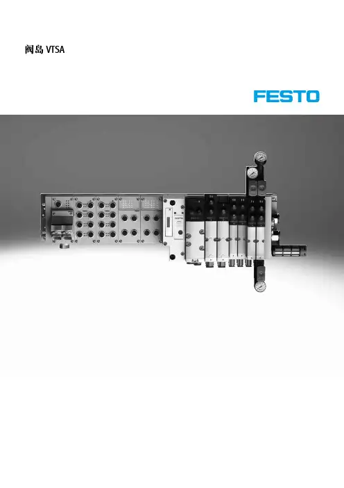
阀岛 VTSA阀岛 VTSA主要特性创新多用途可靠易于安装• 采用坚固金属壳体的高性能阀• 一个阀岛可组合五种阀规格 (阀宽65 mm需连接件)• 标准化的多针插头、现场总线接口和控制模块• 梦之队:总线型阀岛配电气终• 端CPX,强强组合带来:– 前瞻性的内部通信系统,用于控制阀和CPX模块– 一个阀岛可组合四种阀规格而无需连接件– 集成智能阀功能 VTSA-F-CB • 多种阀功能用于集成到更高等级的控制架构中,符合EN ISO 13849-1• 模块化系统,提供一系列配置选项• 最多可扩展至32个电磁线圈• 随时可进行更换和扩展• 集成创新功能模块• 进气板可实现灵活的进气以及可变的压力分区• 逆向工作• 压力范围大 –0.9 ... 10 bar, 流量范围 550 ... 4000 l/min• 多种阀功能• 阀电源 24 V DC阀岛 VTSA-F-CB• 串行通信位于气动部分• 最多 7 个电压分区 (其中 6 个通过 Profisafe 关断模块,一个附加电压分区通过 Uval 实现)• 每个电压区最多 24 片阀• 每个阀岛最多 96 个阀位和最多 64 个互连模块• 坚固耐用的金属元件–– 阀–– 气路板–– 密封件• 通过阀上的LED 快速排除故障,通过现场总线诊断• 阀片可快捷更换,可靠维修• 手控装置,有按钮式、按钮式/锁定式或隐藏式• 采用久经验证的活塞滑阀,耐用• 大而耐用的标签系统• 100% 持续通电率• 装配完毕且经过检测的阀岛,拿到即可安装• 减少选型、订货、安装和调试的费用• 牢固安装在墙面或H型导轨上。
• 通过四个螺丝气路板可以扩展,在金属支撑上的气口隔离非常可靠。
-H- 注意阀宽 65 mm 的主要特性、阀和功能在“适配阀宽 65 mm”ISO3 型一章中另有说明a页码 2262d Internet: /catalogue/...Subject to change – 2023/02阀岛 VTSA 主要特性111312[1] 快速安装: 直接用螺丝安装或H型导轨安装[2] CPX 诊断接口,用于手持式设备(气口和阀片诊断)[3] 气动接口,连接CPX[4] 阀宽 18 mm, 26 mm, 42 mm 和52 mm 可无需适配件就组合在一个阀岛上[5] 减少停机时间: 现场通过LED诊断[6] 可靠操作:手控装置,按钮式,按钮式/锁定式或隐藏式[7] 多用途: 32 个阀位/ 32 个电磁线圈一个阀系列,用于多种流量[8] 阀功能齐全[9] 模块化: 气源板便于创建多个压力分区以及多个额外排气和进气口[10] 实用: 气口口径大,流量优化,坚固的金属螺纹口或预装配QS 接头,用于标准化O.D.的气管[11] 实用:大标签[12] 可靠: 阀、输出和逻辑电压可分别关断[13] 简单的电接口– 现场总线接口连接 CPX– 多针插头接口,带预装配电缆或端子条 (Cage Clamp®)– 控制模块,连接CPX– AS-I 接口– 单个接口– IO-Link– I-Port配备选项阀功能• 2x 两位两通阀, 单电控, 气复位, 常闭• 2x 两位三通阀, 单电控– 常开– 常开, 可逆– 常闭– 常闭, 可逆• 2x 两位三通阀, 单电控– 1x 常开, 1x 常闭– 1x 常开, 1x 常闭, 可逆• 两位五通电磁阀––单电控, 气复位/弹簧复位––双电控––双电控, 带主控信号• 两位五通阀,用于特殊功能,单电控– 弹簧复位– 通过电感式传感器感测开关位置PNP 或 NPN输出– 意外启动保护EN 1037– 逆向工作• 三位五通电磁阀– 中压式– 中封式– 中泄式• 三位五通阀,用于特殊功能– 开关位置14 被保留(开关位置14 被保留,如果紧急停机/断电),开关位置12 无弹簧复位– 仅用于阀岛(插拔式)– 中泄式或中间位置1→2,4→5– 开关位置14 被保留– 气复位• 三位五通阀,用于特殊功能– 开关位置12 被保留(开关位置12 被保留,如果紧急停机/断电),开关位置14 无弹簧复位– 仅用于阀岛(插拔式)– 中泄式或中间位置1→4,2→3– 开关位置12 被保留– 气复位• 软启动阀,用于缓慢而安全地增压– 高度安全– 传感器功能反馈开关位置H--注意阀宽 65 mm 的主要特性、阀和功能在“适配阀宽 65 mm”ISO3 型一章中另有说明a页码 2263 2023/02 – Subject to change d Internet: /catalogue/...阀岛 VTSA主要特性连接选项单阀气路板上的阀, 插拔式单阀气路板上的阀, 方形插头或插拔式• 电接口为标准4针M12 插头或4针弹簧压接端子,用于用户配置• 可用外先导/内先导气源• 集成活塞位置感测• 电接口,符合EN 175301-803 类型C (方形插头) 或• 用于用户配置的4针弹簧压接端子• 开放式电缆现场总线接口 CPX 电气终端现场总线接口 CPX电气终端组合 VTSA-F-CB• 最大32 个阀位/最大32 个电磁线圈• 任意气源• 任意数量的压力分区• 串行通信位于气动部分• 最高4 个电压区,用于气动部分阀的负载电压• 在CPX 接口中可以灵活关断最高3个电压区 , 即可内部通过PROFIsafe 也可外部通过 3x M12实现• 先导开关阀,带集成的压力传感器和内部总线连接• 软启动阀,带集成的压力传感器 和内部总线连接• 真空发生器,三种性能设置,节气回路, 可选增加喷射次数(动力喷射器脉冲) 和 通过内部总线连接, 参数可以通过CPX系统进行配置阀岛,带单个接口阀岛,带多针插头接口AS-I 接口• 最大20 个阀位/最大20 个电磁线圈• 任意气源• 任意数量的压力分区• 最大32 个阀位/最大32 个电磁线圈• 平行的模块化阀链接• 任意气源• 任意数量的压力分区• 1到8 个阀位/最大8 个电磁线圈• 软启动阀,用于缓慢而安全地增压I-Port IO-Link• 最多 16 个阀位/最多 32 个电磁线圈• 连接至一个 I-Port 主站• 直接安装一个总线节点• 最多 16 个阀位/最多 32 个电磁线圈• 连接至一个 IO-Link 主站可组合• 阀宽 18 mm: VTSA 流量最高550 l/min, VTSA-F 流量最高700 l/ min• 阀宽 26 mm: VTSA 流量最高1100 l/min, VTSA-F 流量最高1350 l/min • 阀宽 42 mm: VTSA 流量最高1300 l/min, VTSA-F 流量最高1860 l/min• 阀宽 52 mm: 流量最高2900 l/min• 阀宽 18 mm, 26 mm, 42 mm,52 mm 和 65 mm 可组合在一个阀岛上(用适配件,但不适合VTSA-F-CB)阀岛 VTSA 符合:• ISO 15407-2 阀宽 18 和 26 mm• ISO 5599-2 阀宽 42 和 52 mm4d Internet: /catalogue/...Subject to change – 2023/0252023/02 – Subject to changed Internet: /catalogue/...阀岛 VTSA主要特性阀岛配置器a Internet: 主要信息VTSAVTSA-FVTSA-F-CB阀岛配置器用于帮助您选择适用VTSA 阀岛,更易于订购合适的产品。