
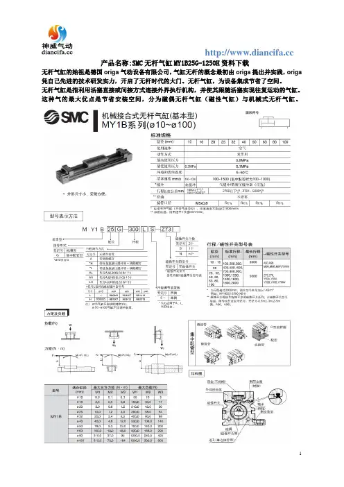
MY1B25G-1250H资料下载
- 格式:doc
- 大小:893.28 KB
- 文档页数:4

FEATURESDESCRIPTIONAPPLICATIONSTYPICAL APPLICATIONbq25010bq25011bq25012SLUS615B–DECEMBER 2004–REVISED JULY 2007SINGLE-CHIP CHARGER AND DC/DC CONVERTER IC FOR PORTABLE APPLICATIONS(bq2501x)•Li-Ion Or Li-Pol Charge Management and Synchronous DC-DC Power Conversion In a The bq2501x series are highly integrated charge and Single Chippower management devices targeted at space-limited bluetooth applications.The bq2501x series offer •Optimized for Powering Bluetooth™Headsets integrated power FET and current sensor for charge and Accessoriescontrol,reverse blocking protection,high accuracy •Charges and Powers the System from Either current and voltage regulation,charge status,charge the AC Adapter or USB with Autonomous termination,and a highly efficient and low-power Power Source Selectiondc-dc converter in a small package.•Integrated USB Charge Control withThe bq2501x charges the battery in three phases:Selectable 100mA and 500mA Charge Rates conditioning,constant current and constant voltage.•Integrated Power FET and Current Sensor for Charge is terminated based on minimum current.An Up to 500mA Charge Applications AND internal charge timer provides a backup safety feature for charge termination.The bq2501x automatically 100mA DC-DC Controller with Integrated re-starts the charge if the battery voltage falls below FETsan internal threshold.The bq2501x automatically •Reverse Leakage Protection Prevents Battery enters sleep mode when V CC supply is removed.DrainageThe integrated low-power high-efficiency dc-dc •Automatic Power Save Mode For Highconverter is designed to operate directly from a Efficiency at Low Current,or Forced PWM for single-cell Li-Ion or Li-Pol battery pack.The output Frequency Sensitive Applications voltage is either adjustable from 0.7V to VBAT •3.5mm ×4.5mm QFN Package(bq25010),fixed at 3.3V (bq25011),or fixed at 1.8V (bq25012),and is capable of delivering up to 150-mA of load current.The dc-dc converter operates at a synchronized 1MHz switching frequency allowing for •Bluetooth™Headsets the use of small inductors.•Bluetooth™Accessories•Low-Power Handheld DevicesPlease be aware that an important notice concerning availability,standard warranty,and use in critical applications of Texas Instruments semiconductor products and disclaimers thereto appears at the end of this data sheet.Bluetooth is a trademark of Bluetooth SIG,Inc.UNLESS OTHERWISE NOTED this document contains Copyright ©2004–2007,Texas Instruments IncorporatedPRODUCTION DATA information current as of publication date.元器件交易网ABSOLUTE MAXIMUM RATINGS (1)RECOMMENDED OPERATING CONDITIONSDISSIPATION RATINGSbq25010bq25011bq25012SLUS615B–DECEMBER 2004–REVISED JULY 2007These devices have limited built-in ESD protection.The leads should be shorted together or the device placed in conductive foam during storage or handling to prevent electrostatic damage to the MOS gates.ORDERING INFORMATION (1)PACKAGE T AOUTPUT VOLTAGE (V)PART NUMBER (2)(3)MARKING Adjustablebq25010RHLR ANC -40°C to 125°C3.3bq25011RHLR (4)ANE 1.8bq25012RHLRANF(1)For the most current package and ordering information,see the Package Option Addendum at the end of this document,or see the TI website at (2)The RHL package is available taped and reeled only in quantities of 3,000devices per reel.(3)This product is RoHS compatible,including a lead concentration that does not exceed 0.1%of total product weight,and is suitable for use in specified lead-free soldering processes.In addition,this product uses package materials that do not contain halogens,including bromine (Br)or antimony (Sb)above 0.1%of total product weight.(4)Advanced Information,contact factory for availability.over operating free-air temperature range (unless otherwise noted)bq25010bq25011bq25012Supply voltage AC,USB (wrt VSS)–0.3V to 7V PG,OUT,ISET1,ISET2,STAT1,STAT2,TS (wrt VSS)–0.3V to 7V Input voltageEN,FB,FPWM,SW (wrt VSS)V OUT +0.3V PG,STAT1,STAT215mA Output sink/source current TS 200μA Output source currentOUT1.5A Storage temperature range,T stg –65°C to 150°C Junction temperature range,T J0°C to 125°CLead temperature (soldering,10seconds)260°C ESD rating (human body model,HBM)1500V(1)Stresses beyond those listed under absolute maximum ratings may cause permanent damage to the device.These are stress ratings only,and functional operation of the device at these or any other conditions beyond those indicated under recommended operating conditions is not implied.Exposure to absolute-maximum-rated conditions for extended periods may affect device reliability.All voltage values are with respect to the network ground terminal unless otherwise noted.MINMAX UNIT V CC Supply voltage (from AC input) 4.5 6.5V V CC Supply voltage (from USB input) 4.35 6.5T JOperating junction temperature range–40125°CT A <40°C DERATING FACTOR PACKAGE θJA POWER RATINGABOVE T A =40°C20-pin RHL (1)1.81W21mW/°C46.87°C/W(1)This data is based on using the JEDEC High-K board and the exposed die pad is connected to a Cu pad on the board.This is connected to the ground plane by a 2׳via matrix.2Submit Documentation Feedback Copyright ©2004–2007,Texas Instruments Incorporated元器件交易网ELECTRICAL CHARACTERISTICSbq25010bq25011bq25012 SLUS615B–DECEMBER2004–REVISED JULY2007over junction temperature range(0°C≤T J≤125°C)and the recommended supply voltage range(unless otherwise noted) PARAMETER TEST CONDITIONS MIN TYP MAX UNITINPUT CURRENTI CC(VCC)Supply current1,VCC V VCC>V VCC(min) 1.22mASum of currents into OUT/BAT,I CC(SLP)Sleep current25V VCC<V(SLP)I CC(STDBY)Stand by current CE=High,0°C≤T J≤85°C150μACharge DONE,V VCC>V VCC(min),I IB(OUT)Input current,OUT1535I OUT(SW)=0mA,Converter not switchingI IB(CE)Input current,CE1CHARGE VOLTAGE REGULATION(V BAT(REG)+V(DO-MAX)≤V VCC,I(TERM)<I OUT(BAT)≤0.5A)V REG(BAT)Charger regulation voltage 4.2VT A=25°C–0.35%0.35%Charge voltage regulationaccuracy–1%1% (V(AC)–V(OUT))AC dropout voltage V OUT(BAT)=V REG(BAT),I OUT(BAT)=0.5A175250V OUT(BAT)=V REG(BAT),ISET2=High350500mV (V(USB)–V(OUT))USB dropout voltageV OUT(BAT)=V REG(BAT),ISET2=Low60100CHARGE CURRENT REGULATIONV VCC≥4.5V,V OUT(BAT)=V(LOWV),I OUT(BAT)AC output current range V VCC–V OUT(BAT)>V(DO-MAX),50500I OUT(BAT)=(K(SET)×V(SET)/R SET)V VCC(min)≥4.5V,V OUT(BAT)=V(LOWV),mA80100V VCC–V OUT(BAT)>V(DO-MAX),ISET2=LowI OUT(BAT)USB output current rangeV VCC(min)≥4.5V,V OUT(BAT)=V(LOWV),400500V VCC–V OUT(BAT)>V(DO-MAX),ISET2=HighVoltage on ISET1,V VCC≥4.5V,V(SET)Output current set voltage V OUT(BAT)=V(LOWV), 2.436 2.500 2.538VV VCC–V OUT(BAT)>V(DO-MAX),ISET2=High50mA≤I OUT(OUT)≤500mA307322337K(SET)Output current set factor10mA≤I OUT(OUT)≤50mA29632034610mA≤I OUT(OUT)≤10mA246320416PRECHARGE and SHORT-CIRCUIT CURRENT REGULATIONPrecharge to fast-chargeV(LOWV)Voltage on OUT/BAT 2.83 3.2V transition thresholdV VCC(min)≥4.5V,t FALL=100ns,Deglitch time for fast-charge tot PRECHG_DG10mV overdrive,250375500ms precharge transitionV IN(BAT)decreasing below threshold0V<V IN(BAT)<V(LOWV),t<t(PRECHG),I OUT(PRECHG)Precharge range5100mAI OUT(PRECHG)=(K(SET)נV(PRECHG))/R SETVoltage on ISET1,V REG(BAT)=4.2V,V(PRECHG)Precharge set voltage0V<V IN(BAT)<V(LOWV),240255270mVt<t(PRECHG)CHARGE TAPER and TERMINATION DETECTIONV IN(BAT)>V(RCH),t<t(PRECHG),I(TAPER)Charge taper detection range5100mAI(TAPER)=(K(SET)נV(TAPER))/R SETCharge taper detection set Voltage on ISET1,V REG(BAT)=4.2V,V(TAPER)235250265voltage V IN(BAT)>V(RCH),t<t(PRECHG)mVVoltage on ISET1,V REG(BAT)=4.2V,Charge termination detectionV(TERM)V IN(BAT)>V(RCH),t<t(PRECHG),111825set voltageI(TERM)=(K(SET)נV(TERM))/R SETCopyright©2004–2007,Texas Instruments Incorporated Submit Documentation Feedback3元器件交易网bq25010bq25011bq25012SLUS615B–DECEMBER 2004–REVISED JULY 2007ELECTRICAL CHARACTERISTICS (continued)over junction temperature range (0°C ≤T J ≤125°C)and the recommended supply voltage range (unless otherwise noted)PARAMETERTEST CONDITIONSMIN TYP MAX UNIT V VCC(min)≥4.5V,t FALL =100ns,Deglitch time for taper t TPRDET_DG10mV overdrive,I CHG increasing above or 250375500detectiondecreasing below threshold msV VCC(min)≥4.5V,t FALL =100ns,Deglitch time for termination t TERMDET_DG10mV overdrive,350375500detectionI CHG decreasing below thresholdBATTERY RECHARGE THRESHOLD V REG(BAT)V REG(BAT)V REG(BAT)V RCH Recharge threshold voltage V –0.115–0.10–0.085V VCC(min)≥4.5V,t FALL =100ns,Deglitch time for recharge t RCHDET10mV overdrive,I CHG decreasing below or 250375500msdetectincreasing above threshold STAT1,STAT2and PG OUTPUTS V OL Low-level output voltage I OL =5mA 0.25VISET2and CE INPUTSV IL Low-level input voltage I IL =10μA 00.4VV IH High-level input voltage I IL =20μA1.4I IL Low-level input current,CE –1I IH High-level input current,CE 1I IL Low-level input current,ISET2V ISET2=0V –20μAI IH High-level input current,ISET2V ISET2=V CC40I IHZ High-Z input current,ISET2V ISET2=High-Z1TIMERS t (PRECHG)Precharge time limit 162018001930t (TAPER)Taper time limit 162018001930s t (CHG)Charge time limit162001800019300I (FAULT)Timer fault recovery current 200μA SLEEP COMPARATOR for CHARGER V VCC ≤V (SLP)Sleep mode entry threshold2.3V ≤V IN(BAT)≤V REG(BAT)V IN(BAT)+80mVVV VCC ≥V (SLP_DG)Sleep mode exit threshold 2.3V ≤V IN(BAT)≤V REG(BAT)V IN(BAT)+190mVV CC decreasing below threshold,t (DEGL)Deglitch time for sleep mode250375500mst FALL =100ns,10mV overdrive,THERMAL SHUTDOWN Thermal trip threshold T (SHTDWN)165temperature °CThermal hysteresis15UNDERVOLTAGE LOCKOUT AND POR Undervoltage lockout V (UVLO_CHG)Decreasing V CC2.42.5 2.6V threshold voltage Hysteresis27mV V POR POR threshold voltage (1)2.32.42.5V(1)Ensured by design.Not production tested.4Submit Documentation Feedback Copyright ©2004–2007,Texas Instruments Incorporated元器件交易网bq25010bq25011bq25012 SLUS615B–DECEMBER2004–REVISED JULY2007ELECTRICAL CHARACTERISTICS(continued)over junction temperature range(0°C≤T J≤125°C)and the recommended supply voltage range(unless otherwise noted) PARAMETER TEST CONDITIONS MIN TYP MAX UNITDC-DC INPUT/OUTPUT CURRENTInput power absent V(LOWV) 4.2V(BAT)Input voltage rangeInput power present V(UVLO) 4.2V UVLOUndervoltage lockout2I OUT_L Maximum output current150mAFPWM–bq25010V IH(FPWM)High-level input voltage 2.0V IL(FPWM)Low-level input voltage0.4FPWM bq25011and bq25012V IH(FPWM)High-level input voltage 1.3V V IL(FPWM)Low-level input voltage0.4I FPWM Input bias current V EN=GND or V BAT,V FPWM=GND or V BAT0.010.1μAENABLEV IH(EN)High-level input voltage 1.3V V IL(EN)Low-level input voltage0.4I EN Input bias current V EN=GND or V BAT,V FPWM=GND or V BAT0.010.1μAPOWER SWITCHV IN=V GS=3.6V0.97 1.52 Internal P-channel MOSFETon-resistance VIN =V GS=2.5V 1.27 2.00R DS(on)ΩV IN=V GS=3.6V0.68 1.19 Internal N-channel MOSFETon-resistance VIN=V GS=2.5V0.86 1.45I lgk(P)P-channel leakage current V DS=6V0.11μA I lgk(N)N-channel leakage current V DS=6V0.11I(LIM)P-channel current limit 2.5V<V BAT<4.2V190230350mAOSCILLATORf SW Switching frequency0.651 1.5MHzOUTPUTV REF Reference voltage bq250100.5Feedback 3.6V≤V BAT≤4.2V,0mA≤I OUT≤150V FB bq25010–3%+3% voltage(2)mAAdjustable outputbq250100.7V BAT voltage range V3.6V≤V BAT≤4.2V,0mA≤I OUT≤150V DC-DC bq25011 3.2 3.3 3.4mAFixed outputvoltage 3.6V≤VBAT ≤4.2V,0mA≤I OUT≤150bq25012 1.746 1.8 1.854mA(2)For output voltages≤1.2V a22-μF output capacitor value is required to achieve a maximum output voltage accuracy of+3%whileoperating in power save mode(PFM).Copyright©2004–2007,Texas Instruments Incorporated Submit Documentation Feedback5元器件交易网TYPICAL OPERATING CHARACTERISTICSE f f i c i e n c y −%I L −Load Current −mAE f f i c i e n c y −%I L −Load Current −mADEVICE INFORMATIONbq25010, bq25011, bq25012RHL PACKAGE (BOTTOM VIEW)SW VSS BAT/OUT BAT/OUTCE PG ISET2ISET1P W M/CN /CN /Cbq25010bq25011bq25012SLUS615B–DECEMBER 2004–REVISED JULY 2007EFFICIENCYEFFICIENCYvsvsLOAD CURRENTFigure 1.Figure 2.6Submit Documentation FeedbackCopyright ©2004–2007,Texas Instruments Incorporated元器件交易网bq25010bq25011bq25012SLUS615B–DECEMBER2004–REVISED JULY2007 TERMINAL FUNCTIONSTERMINALI/O DESCRIPTIONNAME NO.AC5I Charge input voltage from AC adapterBAT/OUT16I/O Charge current outputBAT/OUT17I Battery input to DC-DC converterCE15I Charge enable input(active low)EN4I Enable input for DC-DC converter(active high)FB2I Feedback pin for DC-DC converterPWM control input for the DC-DC converter.A high on FPWM=forced PWM mode.A low=power save FPWM20Imode.ISET112I Charge current set point for AC input and precharge and taper set point for both AC and USBISET213I Charge current set point for USB port(High=500mA,Low=100mA,High-Z=disable USB charge)NC1,10,11–No connect.These pins must be left floating.PG14O Power good status output(active low)STAT17O Charge status output1(open-drain)STAT28O Charge status output2(open-drain)SW19O Phase node of the DC-DC converterUSB6I Charge input voltage from USB adapterGround Input.Also note that there is an internal electrical connection between the exposed thermal padand VSS pins of the device.The exposed thermal pad must be connected to the same potential as the VSS3,9,18–Vss pin on the printed circuit board.Do not use the thermal pad as the primary ground input for thedevice.All VSS pins must be connected to ground at all times.Copyright©2004–2007,Texas Instruments Incorporated Submit Documentation Feedback7元器件交易网ACUSBVSSEN FPWMVSS VSS UDG−04072bq25010bq25011bq25012SLUS615B–DECEMBER 2004–REVISED JULY 2007FUNCTIONAL BLOCK DIAGRAM8Submit Documentation Feedback Copyright ©2004–2007,Texas Instruments Incorporated元器件交易网FUNCTIONAL DESCRIPTIONSBATTERYCHARGERUDG_04095_lus615Status Signalsbq25010bq25011bq25012SLUS615B–DECEMBER 2004–REVISED JULY 2007The bq2501x supports a precision Li-Ion or Li-Pol charging system suitable for single-cell battery packs and a low-power DC-DC converter for providing power to system processor.See a typical charge profile,application circuit and an operational flow chart in Figure 3through Figure 5respectively.Figure 3.Typical Charger ProfileFigure 4.Typical Application CircuitCopyright ©2004–2007,Texas Instruments IncorporatedSubmit Documentation Feedback 9元器件交易网bq25010bq25011bq25012SLUS615B–DECEMBER 2004–REVISED JULY 2007Figure 5.Operational Flow Chart10Submit Documentation Feedback Copyright ©2004–2007,Texas Instruments Incorporated元器件交易网Autonomous Power Source SelectionUSB > BATTERY Battery Pre-ConditioningI O(PRECHG)+V(PRECHG)K(SET)R SET(1)Battery Charge CurrentI O(OUT)+V(SET)K(SET)R SET(2)Battery Voltage RegulationCharge Taper Detection,Termination and Rechargebq25010bq25011bq25012 SLUS615B–DECEMBER2004–REVISED JULY2007As default,the bq2501x attempts to charge the battery from the AC input.If AC input is not present,the USB input is selected.If both inputs are available,the AC adapter has the priority.Refer to Figure6for details.Figure6.Power Source SelectionDuring a charge cycle if the battery voltage is below the V(LOWV)threshold,the bq2501x applies a precharge current,I O(PRECHG),to the battery.This feature revives deeply discharged cells.The resistor connected between the ISET1and VSS pins,R SET,determines the precharge rate.The V(PRECHG)and K(SET)parameters are specified in the specifications table.The bq2501x activates a safety timer,t(PRECHG),during the conditioning phase.If V(LOWV)threshold is not reached within the timer period,the bq2501x turns off the charger and enunciates FAULT on the STAT1and STAT2pins.Please refer to Timer Fault Recovery section for additional details.The bq2501x offers on-chip current regulation with programmable set point.The resistor connected between the ISET1and VSS pins,R SET,determines the charge rate.The V(SET)and K(SET)parameters are specified in the specifications table.When charging from a USB port,the host controller has the option of selecting either100mA or500mA charge rate using the ISET2pin.A low-level signal sets the current at100mA and a high-level signal sets the current at 500mA.A high-Z input disables USB charging.The voltage regulation feedback is through the BAT/OUT pin.This input is tied directly to the positive side of the battery pack.The bq2501x monitors the battery-pack voltage between the BAT/OUT and VSS pins.When the battery voltage rises to V O(REG)threshold,the voltage regulation phase begins and the charging current begins to taper down.As a safety backup,the bq2501x also monitors the charge time in the charge mode.If taper threshold is not detected within this time period,t(CHG),the bq2501x turns off the charger and enunciates FAULT on the STAT1 and STAT2pins.Please refer to section titled Timer Fault Recovery section for additional details.The bq2501x monitors the charging current during the voltage regulation phase.Once the taper threshold, I(TAPER),is detected the bq2501x initiates the taper timer,t(TAPER).Charge is terminated after the timer expires.The resistor connected between the ISET1and VSS pins,R SET,determines the taper detection level.The V(TAPER)and K(SET)parameters are specified in the specifications table.Note that this applies to both AC and USB charging.Copyright©2004–2007,Texas Instruments Incorporated Submit Documentation Feedback11元器件交易网I (TAPER)+V (TAPER) K (SET)R SET(3)I (TERM)+V (TERM) K (SET)R SET(4)Sleep Mode for ChargerOperation ModesStatus OutputsPG Output (Power Good)bq25010bq25011bq25012SLUS615B–DECEMBER 2004–REVISED JULY 2007The bq2501x resets the taper timer in the event that the charge current returns above the taper threshold,I (TAPER).In addition to the taper current detection,the bq2501x terminates charge in the event that the charge current falls below the I (TERM)threshold.This feature allows for quick recognition of a battery removal condition or insertion of a fully charged battery.Note that taper timer is not activated.The resistor connected between the ISET1and VSS pins,R SET ,determines the taper detection level.The V (TERM)and K (SET)parameters are specified in the specifications table.Note that this applies to both AC and USB charging.After charge termination,the bq2501x restarts the charge once the voltage on the BAT/OUT pin falls below the V (RCH)threshold.This feature keeps the battery at full capacity at all times.The bq2501x enters the low-power sleep mode if both AC and USB are removed from the circuit.This feature prevents draining the battery during the absence of V CC .Operational modes of the bq2501x are summarized in Table 1.Operation of DC-DC is not recommended while charger is in precharge mode.Table 1.Operation ModesBATTERY VOLTAGE AC or USB ADAPTER STATUSCHARGER STATUSDC-DC STATUSV I(BAT)>V (LOWV)Present Fast EN 0V <V I(BAT)<V (LOWV)Present PrechargeEN V I(BAT)<V (UVLO)Both absentOffOffThe STAT1and STAT2open-drain outputs indicate various charger and battery conditions as shown in Table 2.These status pins can be used to communicate to the host processor.Note that OFF indicates the transistor is turned off.Table 2.Status Pins SummaryCHARGE STATE INPUT POWER STATESTAT1STAT2Precharge in progress Present ON ON Fast charge in progressPresent ON OFF Charge done Not reported OFF ON Timer fault Not reported OFF OFF Speel modeAbsentOFFOFFThe open-drain PG output indicates when the AC adapter is present.The output turns ON when a valid voltage is detected.This output is turned off in the sleep mode.The PG pin can be used to drive an LED or communicate to the host processor.12Submit Documentation Feedback Copyright ©2004–2007,Texas Instruments Incorporated元器件交易网CE Input(Charge Enable) Thermal Shutdown and Protection Timer Fault RecoveryDC-DC CONVERTERPower Save Mode Operationbq25010bq25011bq25012 SLUS615B–DECEMBER2004–REVISED JULY2007The CE digital input is used to enable or disable the charge process.A low-level signal on this pin enables the charge and a high-level signal disables the charge and places the device into a low-power mode.A high-to-low transition on this pin also resets all timers and timer fault conditions.Note that this applies to both AC and USB charging.The bq2501x monitors the junction temperature,T J,of the die and suspends charging if T J exceeds T(SHTDWN).Charging resumes when T J falls below T(SHTDWN)by approximately15°C.As shown in Figure5,bq2501x provides a recovery method to deal with timer fault conditions.The following summarizesCondition1:Charge voltage above recharge threshold(V(RCH))and timeout fault occurs.Recovery method:bq2501x waits for the battery voltage to fall below the recharge threshold.This could happen as a result of a load on the battery,self-discharge or battery removal.Once the battery falls below the recharge threshold,the bq2501x clears the fault and starts a new charge cycle.A POR or CE toggle also clears the fault.Condition2:Charge voltage below recharge threshold(V(RCH))and timeout fault occurs.Recovery method:Under this scenario,the bq2501x applies the I(FAULT)current.This small current is used to detect a battery removal condition and remains on as long as the battery voltage stays below the recharge threshold.If the battery voltage goes above the recharge threshold,then the bq2501x disables the I(FAULT)current and executes the recovery method described for Condition 1.Once the battery falls below the recharge threshold,the bq2501x clears the fault and starts a new charge cycle.A POR or CE toggle also clears the fault.The bq2501x provides a low quiescent-current synchronous DC-DC converter.The internally compensated converter is designed to operate over the entire voltage range of a single-cell Li-Ion or Li-Pol battery.Under nominal load current,the device operates with a fixed PWM switching frequency of typically1MHz.At light load currents,the device enters the power save mode of operation;the switching frequency is reduced and the quiescent current drawn by the converter from the BAT/OUT pin is typically only15μA.During PWM operation the converter uses a unique fast-response voltage mode controller scheme with input voltage feedforward to achieve good line and load regulation allowing the use of small ceramic input and output capacitors.At the beginning of each clock cycle initiated by the clock signal(S),the P-channel MOSFET switch is turned on and the inductor current ramps up until the comparator trips and the control logic turns off the switch.The current limit comparator also turns off the switch in case the current limit of the P-channel switch is exceeded.After the dead time preventing current shoot through the N-cannel MOSFET rectifier is turned on and the inductor current ramps down.The next cycle is initiated by the clock signal again turning off the N-channel rectifier and turning on the on the P-channel switch.The g M amplifier as well as the input voltage determines the rise time of the saw-tooth generator and therefore any change in input voltage or output voltage directly controls the duty cycle of the converter giving a very good line and load transient regulation.As the load current decreases,the converter enters the power save mode operation.During power save mode, the converter operates with reduced switching frequency in PFM mode and with a minimum quiescent current to maintain high efficiency.Two conditions allow the converter to enter the power save mode operation.One is the detection of discontinuous conduction mode.The other is when the peak switch current in the P-channel switch goes below the skip current limit.The typical skip current limit can be calculated as:Copyright©2004–2007,Texas Instruments Incorporated Submit Documentation Feedback13元器件交易网I SKIP +66mA )V IN 160W(5)I PEAK +66mA )VIN80W (6)PFM Mode at Light LoadComparator High Comparator Low Comparator Low 2PWM Mode at Medium to Full Load1.6%0.8%V OUTDynamic Voltage PositioningSoft-Startbq25010bq25011bq25012SLUS615B–DECEMBER 2004–REVISED JULY 2007During the power save mode,the output voltage is monitored with the comparator by the thresholds comp low and comp high.As the output voltage falls below the comp low threshold (set to typically 0.8%above VOUT nominal),the P-channel switch turns on.The P-channel switch is turned off as the peak switch current is reached.The typical peak switch current can be calculated as:The N-channel rectifier is turned on and the inductor current ramps down.As the inductor current approacheszero,the N-channel rectifier is turned off,and the P-channel switch is turned on starting the next pulse.The converter continues these pulses until the comp high threshold (set to typically 1.6%above VOUT nominal)is reached.The converter enters a sleep mode,reducing the quiescent current to a minimum.The converter wakes up again as the output voltage falls below the comp low threshold again.This control method reduces the quiescent current to typically to 15μA and the switching frequency to a minimum;thereby,achieving high converter efficiency.Setting the skip current thresholds to typically 0.8%and 1.6%above the nominal output voltage at light load current results in a dynamic output voltage achieving lower absolute voltage drops during heavy load transient changes.This allows the converter to operate with a small output capacitor of only 10μF and still have a low absolute voltage drop during heavy load transient changes.Refer to Figure 7as well for detailed operation of the power save mode.Figure 7.Power Save Mode Thresholds and Dynamic Voltage PositioningThe converter enters the fixed-frequency PWM mode again as soon as the output voltage drops below the comp low 2threshold.As described in the power save mode operation section and as detailed in Figure 7,the output voltage is typically 0.8%above the nominal output voltage at light load currents as the save mode.This gives additional headroom for the voltage drop during a load transient from light load to full load.During a load transient from full load to light load the voltage overshoot is also minimized due to active regulation turning on the N-Channel rectifier switch.The bq2501x has an internal soft-start circuit that limits the inrush current during startup.This soft-start is implemented as a digital circuit increasing the switch current in steps of typically 30mA,60mA,120mA and then the typical switch current limit of 230mA.Therefore the startup time depends mainly on the output capacitor and load current.Typical startup time with a 10-μF output capacitor and a 100-mA load current is 1.6ms.14Submit Documentation Feedback Copyright ©2004–2007,Texas Instruments Incorporated元器件交易网。

FEATURES DESCRIPTIONAPPLICATIONSbq25010bq25011bq25012SLUS615–DECEMBER2004 SINGLE-CHIP CHARGER AND DC/DC CONVERTER IC FOR BLUETOOTH HEADSETSAND OTHER PORTABLE APPLICATIONS(bqHYBRID™)•Li-Ion Or Li-Pol Charge Management and The bqHYBRID™series are highly integrated charge Synchronous DC-DC Power Conversion In a and power management devices targeted atSingle Chip space-limited bluetooth applications.The bqHYBRIDseries offer integrated power FET and current sensor •Optimized for Powering Bluetooth Headsetsfor charge control,reverse blocking protection,high and Accessoriesaccuracy current and voltage regulation,charge •Charges and Powers the System from Either status,charge termination,and a highly efficient and the AC Adapter or USB with Autonomous low-power dc-dc converter in a small package.Power Source SelectionThe bqHYBRID charges the battery in three phases:•Integrated USB Charge Control with conditioning,constant current and constant voltage.Selectable100mA and500mA Charge Rates Charge is terminated based on minimum current.An •Integrated Power FET and Current Sensor for internal charge timer provides a backup safety featurefor charge termination.The bqHYBRID automatically Up to500mA Charge Applications ANDre-starts the charge if the battery voltage falls below 100mA1.8V DC-DC Controller withan internal threshold.The bqHYBRID automatically Integrated FETenters sleep mode when V CC supply is removed.•Reverse Leakage Protection Prevents BatteryThe integrated low-power high-efficiency dc-dc con-Drainageverter is designed to operate directly from a •Automatic Power Save Mode For Highsingle-cell Li-Ion or Li-Pol battery pack.The output Efficiency at Low Current,or Forced PWM for voltage is either adjustable from0.7V to VBATFrequency Sensitive Applications(bq25010),fixed at3.3V(bq25011),or fixed at1.8V(bq25012),and is capable of delivering up to150-mAof load current.The dc-dc converter operates at asynchronized1MHz switching frequency allowing for •Bluetooth Headsetsthe use of small inductors.•Bluetooth Accessories•Low-Power Handheld DevicesTYPICAL APPLICATIONPlease be aware that an important notice concerning availability,standard warranty,and use in critical applications of TexasInstruments semiconductor products and disclaimers thereto appears at the end of this data sheet.bqHYBRID is a trademark of Benchmark.PRODUCTION DATA information is current as of publication date.Copyright©2004,Texas Instruments Incorporated Products conform to specifications per the terms of the TexasInstruments standard warranty.Production processing does notnecessarily include testing of all parameters.元器件交易网ABSOLUTE MAXIMUM RATINGS (1)RECOMMENDED OPERATING CONDITIONSDISSIPATION RATINGSbq25010bq25011bq25012SLUS615–DECEMBER 2004These devices have limited built-in ESD protection.The leads should be shorted together or the device placed in conductive foam during storage or handling to prevent electrostatic damage to the MOS gates.ORDERING INFORMATIONPACKAGE T AOUTPUT VOLTAGE (V)PART NUMBER (1)(2)MARKING Adjustablebq25010RHLR ANC -40°C to 125°C3.3bq25011RHLR (3)ANE 1.8bq25012RHLR (3)ANF(1)The RHL package is available taped and reeled only in quantities of 3,000devices per reel.(2)This product is RoHS compatible,including a lead concentration that does not exceed 0.1%of total product weight,and is suitable for use in specified lead-free soldering processes.In addition,this product uses package materials that do not contain halogens,including bromine (Br)or antimony (Sb)above 0.1%of total product weight.(3)Advanced Information,contact factory for availability.over operating free-air temperature range (unless otherwise noted)bq25010bq25011bq25012Supply voltage AC,USB (wrt VSS)–0.3V to 7V PG,OUT,ISET1,ISET2,STAT1,STAT2,TS (wrt VSS)–0.3V to 7V Input voltageEN,FB,FPWM,SW (wrt VSS)V OUT +0.3V PG,STAT1,STAT215mA Output sink/source current TS 200µA Output source currentOUT1.5A Storage temperature range,T stg –65°C to 150°C Junction temperature range,T J0°C to 125°CLead temperature (solderig,10seconds)260°C(1)Stresses beyond those listed under absolute maximum ratings may cause permanent damage to the device.These are stress ratings only,and functional operation of the device at these or any other conditions beyond those indicated under recommended operating conditions is not implied.Exposure to absolute-maximum-rated conditions for extended periods may affect device reliability.All voltage values are with respect to the network ground terminal unless otherwise noted.MINMAX UNIT V CC Supply voltage (from AC input) 4.5 6.5V V CC Supply voltage (from USB input) 4.35 6.5T JOperating junction temperature range–40125°CT A <40°C DERATING FACTOR PACKAGE θJA POWER RATINGABOVE T A =40°C20-pin RHL (1)1.81W21mW/°C46.87°C/W(1)This data is based on using the JEDEC High-K board and the exposed die pad is connected to a Cu pad on the board.This is connected to the ground plane by a 2×3via matrix.2元器件交易网ELECTRICAL CHARACTERISTICSbq25010bq25011bq25012 SLUS615–DECEMBER2004over junction temperature range(0°C≤TJ≤125°C)and the recommended supply voltage range(unless otherwise noted) PARAMETER TEST CONDITIONS MIN TYP MAX UNITINPUT CURRENTI CC(VCC)Supply current1,VCC V VCC>V VCC(min) 1.2 2.0mASum of currents into OUT/BAT,I CC(SLP)Sleep current25V VCC<V(SLP)I CC(STDBY)Standyby current CE=High,0°C≤T J≤85°C150µACharge DONE,V VCC>V VCC(min),I IB(OUT)Input current,OUT1535I OUT(SW)=0mA,Converter not switchingI IB Input current,CE1CHARGE VOLTAGE REGULATION(V BAT(REG)+V(DO-MAX)≤V VCC,I(TERM)<I OUT(BAT)≤0.5A)V REG(BAT)Charger output voltage 4.2VT A=25°C–0.35%0.35%Charge voltage regulationaccuracy–1%1% (V(AC)–V(OUT))AC dropout voltage V OUT(BAT)=V REG(BAT),I OUT(BAT)=0.5A175250V OUT(BAT)=V REG(BAT),ISET2=High350500mV (V(USB)–V(OUT))USB dropout voltageV OUT(BAT)=V REG(BAT),ISET2=Low60100CHARGE CURRENT REGULATIONV VCC≥4.5V,V OUT(BAT)=V(LOWV),I OUT(BAT)AC output current range V VCC–V OUT(BAT)>V(DO-MAX),50500I OUT(BAT)=(K(SET)×V(SET)/R SET)V VCC(min)≥4.5V,V OUT(BAT)=V(LOWV),mA80100V VCC–V OUT(BAT)>V(DO-MAX),ISET2=LowI OUT(BAT)USB output current rangeV VCC(min)≥4.5V,V OUT(BAT)=V(LOWV),400500V VCC–V OUT(BAT)>V(DO-MAX),ISET2=HighVoltage on ISET1,V VCC≥4.5V,V(SET)Output current set voltage V OUT(BAT)=V(LOWV), 2.436 2.500 2.538VV VCC–V OUT(BAT)>V(DO-MAX),ISET2=High50mA≤I OUT(OUT)≤500mA307322337 K(SET)Output current set factor10mA≤I OUT(OUT)≤50mA29632034610mA≤I OUT(OUT)≤10mA246320416 PRECHARGE and SHORT-CIRCUIT CURRENT REGULATIONPrecharge to fast-charge tran-V(LOWV)Voltage on OUT/BAT 2.8 3.0 3.2V sition thresholdV VCC(min)≥4.5V,t FALL=100ns,Deglitch time for fast-charge tot PRECHG_DG10mV overdrive,250375500ms precharge transitionV IN(BAT)decreasing below threshold0V<V IN(BAT)<V(LOWV),t<t(PRECHG),I OUT(PRECHG)Precharge range5100mAI OUT(PRECHG)=(K(SET)×V(PRECHG))/R SETVoltage on ISET1,V REG(BAT)=4.2V,V(PRECHG)Precharge set voltage0V<V IN(BAT)<V(LOWV),240255270mVt<t(PRECHG)CHARGE TAPER and TERMINATION DETECTIONV IN(BAT)>V(RCH),t<t(PRECHG),I(TAPER)Charge taper detection range5100mAI(TAPER)=(K(SET)×V(TAPER))/R SETCharge taper detection set Voltage on ISET1,V REG(BAT)=4.2V,V(TAPER)235250265voltage V IN(BAT)>V(RCH),t<t(PRECHG)mVVoltage on ISET1,V REG(BAT)=4.2V,Charge termination detectionV(TERM)V IN(BAT)>V(RCH),t<t(PRECHG),111825set voltageI(TERM)=(K(SET)×V(TERM))/R SET3元器件交易网bq25010bq25011bq25012SLUS615–DECEMBER 2004ELECTRICAL CHARACTERISTICS (continued)over junction temperature range (0°C ≤T J ≤125°C)and the recommended supply voltage range (unless otherwise noted)PARAMETERTEST CONDITIONSMIN TYP MAX UNIT V VCC(min)≥4.5V,t FALL =100ns,Deglitch time for taper detec-t TPRDET_DG10mV overdrive,I CHG increasing above or 250375500tiondecreasong below threshold msV VCC(min)≥4.5V,t FALL =100ns,Deglitch time for termination t TERMDET_DG10mV overdrive,350375500detectionI CHG decreasing below thresholdBATTERY RECHARGE THRESHOLD V REG(BAT)V REG(BAT)V REG(BAT)V RCH Recharge threshold voltage V –0.115–0.10–0.085V VCC(min)≥4.5V,t FALL =100ns,Deglitch time for recharge de-t RCHDET10mV overdrive,I CHG decreasing below or 250375500mstectincreasing above threshold STAT1,STAT2and PG OUTPUTS V OL Low-level output voltage I OL =5mA 0.25VISET2and CE INPUTSV IL Low-level input voltage I IL =10µA 00.4VV IH High-level input voltage I IL =20µA1.4I IL Low-level input current,CE –1I IH High-level input current,CE 1I IL Low-level input current,ISET2V ISET2=0V –20µAI IH High-level input current,ISET2V ISET2=V CC40I IHZ High-Z input current,ISET2V ISET2=High-Z1TIMERS t (PRECHG)Precharge time 162018001930t (TAPER)Taper time 162018001930s t (CHG)Charge time162001800019300I (FAULT)Timer fault recovery current 200µA SLEEP COMPARATOR for CHARGER V VCC ≤V (SLP)Sleep mode entry threshold2.3V ≤V IN(BAT)≤V REG(BAT)V IN(BAT)+80mVVV VCC ≥V (SLP_DG)Sleep mode exit threshold 2.3V ≤V IN(BAT)≤V REG(BAT)V IN(BAT)+190mVV CC decreasing below threshold,t (DEGL)Deglitch time for sleep mode250375500mst FALL =100ns,10mV overdrive,THERMAL SHUTDOWN Thermal trip threshold tem-T (SHTDWN)165perature°CThermal hysteresis15UNDERVOLTAGE LOCKOUT AND POR Undervoltage lockout V (UVLO_CHG)Decreasing V CC2.42.5 2.6V threshold voltage Hysteresis27mV V PORPOR threshold voltage (1)2.3 2.42.5VDC-DC INPUT/OUTPUT CURRENT Input power absent V (LOWV) 4.2V (BAT)Input voltage range Input power presentV (UVLO)4.2VV (UVLO)Undervoltage lockout2.0(1)Ensured by design.Not production tested.4元器件交易网bq25010bq25011bq25012 SLUS615–DECEMBER2004ELECTRICAL CHARACTERISTICS(continued)over junction temperature range(0°C≤TJ≤125°C)and the recommended supply voltage range(unless otherwise noted) PARAMETER TEST CONDITIONS MIN TYP MAX UNITI OUT_L Maximum output current150mAFPWM–bq25010V IH(FPWM)High-level input voltage 2.0V IL(FPWM)Low-level input voltage0.4FPWM bq25011and bq25012V IH(FPWM)High-level input voltage 1.3V V IL(FPWM)Low-level input voltage0.4I FPWM Input bias current V EN=GND or V BAT,V FPWM=GND or V BAT0.010.1µAENABLEV IH(EN)High-level input voltage 1.3V V IL(EN)Low-level input voltage0.4I EN Input bias current V EN=GND or V BAT,V FPWM=GND or V BAT0.010.1µAPOWER SWITCHV IN=V GS=3.6V0.97 1.52 Internal P-channel MOSFETon-resistance VIN =V GS=2.5V 1.27 2.00R DS(on)ΩV IN=V GS=3.6V0.68 1.19Internal N-channel MOSFETon-resistance VIN=V GS=2.5V0.86 1.45I LEAK(P)P-channel leakage current V DS=6.0V0.1 1.0µAI LEAK(N)N-channel leakage current V DS=6.0V0.1 1.0I(LIM)P-channel current limit 2.5V<V BAT<4.2V190230350mA OSCILLATORf SW Switching frequency0.65 1.00 1.50MHzOUTPUTV REF Reference voltage bq250100.5Feedback volt-V FB bq25010 3.6V≤V BAT≤4.2V,0mA≤I OUT≤150mA–3%+3%age(2)Adjustable output Vbq250100.7V BATvoltage rangeV DC-DCbq25011 3.6V≤V BAT≤4.2V,0mA≤I OUT≤150mA 3.2 3.3 3.4Fixed output volt-age bq25012 3.6V≤VBAT≤4.2V,0mA≤I OUT≤150mA 1.746 1.8 1.854(2)For output voltages≤1.2V a22-µF output capacitor value is required to achieve a maximum output voltage accuracy of+3%whileoperating in power save mode(PFM).5元器件交易网DEVICE INFORMATIONbq25010, bq25011, bq25012RHL PACKAGE (BOTTOM VIEW)SW VSS BAT/OUT BAT/OUTCE PG ISET2ISET1P W M/CN /CN /Cbq25010bq25011bq25012SLUS615–DECEMBER 2004TERMINAL FUNCTIONSTERMINAL I/O DESCRIPTIONNAME NO.AC 5I Charge input voltage from AC adapter BAT/OUT 16I/O Charge current outputBAT/OUT 17I Battery input to DC-DC converter CE 15I Charge enable input (active low)EN 4I Enable input for DC-DC converter FB 2I Feedback pin for DC-DC converter FPWM 20I PWM control input for the DC-DC converterISET112I Charge current set point for AC input and precharge and taper set point for both AC and USB ISET213I Charge current set point for USB port (High =500mA,Low =100mA,High-Z =disable USB charge)NC 1,10,11–No connect.These pins must be left floating.PG 14O Power good status output (active low)STAT17O Charge status output 1(open-drain)STAT28O Charge status output 2(open-drain)SW 19O Output of the DC/DC converter USB 6I Charge input voltage from USB adapterGround Input.Also note that there is an internal electrical connection between the exposed thermal pad and VSS pins of the device.The exposed thermal pad must be connected to the same potential as the VSS3,9,18–Vss pin on the printed circuit board.Do not use the thermal pad as the primary ground input for the device.All VSS pins must be connected to ground at all times.6元器件交易网ACUSBVSSEN FPWMVSS VSS UDG−04072bq25010bq25011bq25012SLUS615–DECEMBER 2004FUNCTIONAL BLOCK DIAGRAM7元器件交易网FUNCTIONAL DESCRIPTIONSBATTERY CHARGERRegulationVoltage RegulationCurrentMinimum Charge VoltagePre-Conditioning and Taper DetectStatus SignalsUDG−04095bq25010bq25011bq25012SLUS615–DECEMBER 2004The bqHYBRID supports a precision Li-Ion or Li-Pol charging system suitable for single-cell battery packs and a low-power DC-DC converter for providing power to system processor.See a typical charge profile,application circuit and an operational flow chart in Figure 1through Figure 3respectively.Figure 2.Typical Application Circuit8元器件交易网bq25010bq25011bq25012 SLUS615–DECEMBER2004FUNCTIONAL DESCRIPTIONS(continued)Figure3.Operational Flow Chart9元器件交易网Autononous Power Source SelectionUSB > BATTERYBattery Pre-ConditioningI O (PRECHG)+V (PRECHG) K (SET)R SET(1)Battery Charge CurrentI O (OUT)+V (SET) K (SET)R SET(2)Battery Voltage RegulationCharge Taper Detection,Termination and Reghargebq25010bq25011bq25012SLUS615–DECEMBER 2004FUNCTIONAL DESCRIPTIONS (continued)As default,the bqHYBRID attempts to charge the battery from the AC input.If AC input is not present,the USB input is selected.If both inputs are available,the AC adapter has the priority.Refer to Figure 4for details.Figure 4.Power Source SelectionDuring a charge cycle if the battery voltage is below the V (LOWV)threshold,the bqHYBRID applies a precharge current,I O(PRECHG),to the battery.This feature revives deeply discharged cells.The resistor connected between the ISET1and VSS pins,R SET ,determines the precharge rate.The V (PRECHG)and K (SET)parameters are specified in the specifications table.The bqHYBRID activates a safety timer,t (PRECHG),during the conditioning phase.If V (LOWV)threshold is not reached within the timer period,the bqHYBRID turns off the charger and enunciates FAULT on the STAT1and STAT2pins.Please refer to Timer Fault Recovery section for additional details.The bqHYBRID offers on-chip current regulation with programmable set point.The resistor connected between the ISET1and VSS pins,R SET ,determines the charge rate.The V (SET)and K (SET)parameters are specified in the specifications table.When charging from a USB port,the host controller has the option of selecting either 100mA or 500mA charge rate using the ISET2pin.A low-level signal sets the current at 100mA and a high-level signal sets the current at 500mA.A high-Z input disables USB charging.The voltage regulation feedback is through the BAT/OUT pin.This input is tied directly to the positive side of the battery pack.The bqHYBRID monitors the battery-pack voltage between the BAT/OUT and VSS pins.When the battery voltage rises to V O(REG)threshold,the voltage regulation phase begins and the charging current begins to taper down.As a safety backup,the bqHYBRID also monitors the charge time in the charge mode.If taper threshold is not detected within this time period,t (CHG),the bqHYBRID turns off the charger and enunciates FAULT on the STAT1and STAT2pins.Please refer to section titled Timer Fault Recovery section for additional details.The bqHYBRID monitors the charging current during the voltage regulation phase.Once the taper threshold,I (TAPER),is detected the bqHYBRID initiates the taper timer,t (TAPER).Charge is terminated after the timer expires.The resistor connected between the ISET1and VSS pins,R SET ,determines the taper detection level.The V (TAPER)and K (SET)parameters are specified in the specifications table.Note that this applies to both AC and USB charging.10元器件交易网I(TAPER)+V(TAPER)K(SET)R SET(3)I(TERM)+V(TERM)K(SET)R SET(4)Sleep Mode for Charger Operation ModesStatus OutputsPG Output(Power Good)bq25010bq25011bq25012 SLUS615–DECEMBER2004FUNCTIONAL DESCRIPTIONS(continued)The bqHYBRID resets the taper timer in the event that the charge current returns above the taper threshold, I(TAPER).In addition to the taper current detection,the bqHYBRID terminates charge in the event that the charge current falls below the I(TERM)threshold.This feature allows for quick recognition of a battery removal condition or insertion of a fully charged battery.Note that taper timer is not activated.The resistor connected between the ISET1and VSS pins,R SET,determines the taper detection level.The V(TERM)and K(SET)parameters are specified in the specifications table.Note that this applies to both AC and USB charging.After charge termination,the bqHYBRID restarts the charge once the voltage on the BAT/OUT pin falls below the V(RCH)threshold.This feature keeps the battery at full capacity at all times.The bqHYBRID enters the low-power sleep mode if both AC and USB are removed from the circuit.This feature prevents draining the battery during the absence of V CC.Operational modes of the bqHYBRID are summarized in Table1.Operation of DC-DC is not recommended while charger is in precharge mode.Table1.Operation ModesBATTERY VOLTAGE AC or USB ADAPTER STATUS CHARGER STATUS DC-DC STATUS V I(BAT)>V(LOWV)Present Fast EN 0V<V I(BAT)<V(LOWV)Present Precharge EN V I(BAT)<V(UVLO)Both absent Off OffThe STAT1and STAT2open-drain outputs indicate various charger and battery conditions as shown in Table2.These status pins can be used to communicate to the host processor.Note that OFF indicates the open-drain transistor is turned off.Table2.Status Pins SummaryCHARGE STATE INPUT POWER STATE STAT1STAT2Precharge in progress Present ON ONFast charge in progress Present ON OFF Charge done Not reported OFF ONTimer fault Not reported OFF OFFSpeel mode Absent OFF OFFThe open-drain PG output indicates when the AC adapter is present.The output turns ON when a valid voltage is detected.This output is turned off in the sleep mode.The PG pin can be used to drive an LED or communicate to the host processor.11元器件交易网 CE Input (Charge Enable)Thermal Shutdown and ProtectionTImer Fault RecoveryDC-DC CONVERTERPower Save Mode Operationbq25010bq25011bq25012SLUS615–DECEMBER 2004The CE digital input is used to enable or disable the charge process.A low-level signal on this pin enables the charge and a high-level signal disables the charge and places the device into a low-power mode.A high-to-low transition on this pin also resets all timers and timer fault conditions.Note that this applies to both AC and USB charging.The bqHYBRID monitors the junction temperature,T J ,of the die and suspends charging if T J exceeds T (SHTDWN).Charging resumes when T J falls below T (SHTDWN)by approximately 15°C.As shown in Figure 3,bqHYBRID provides a recovery method to deal with timer fault conditions.The following summarizes this method:Condition 1:Charge voltage above recharge threshold (V (RCH))and timeout fault occurs.Recovery method:bqHYBRID waits for the battery voltage to fall below the recharge threshold.This could happen as a result of a load on the battery,self-discharge or battery removal.Once the battery falls below the recharge threshold,the bqHYBRID clears the fault and starts a new charge cycle.A POR or CE toggle also clears the fault.Condition 2:Charge voltage below recharge threshold (V (RCH))and timeout fault occurs.Recovery method:Under this scenario,the bqHYBRID applies the I (FAULT)current.This small current is used to detect a battery removal condition and remains on as long as the battery voltage stays below the recharge threshold.If the battery voltage goes above the recharge threshold,then the bqHYBRID disables the I (FAULT)current and executes the recovery method described for Condition 1.Once the battery falls below the recharge threshold,the bqHYBRID clears the fault and starts a new charge cycle.A POR or CE toggle also clears the fault.The bqHYBRID provides a low quiescent-current synchronous DC-DC converter.The internally compensated converter is designed to operate over the entire voltage range of a single-cell Li-Ion or Li-Pol battery.Under nominal load current,the device operates with a fixed PWM switching frequency of typically 1MHz.At light load currents,the device enters the power save mode of operation;the switching frequency is reduced and the quiescent current drawn by the converter from the BAT/OUT pin is typically only 15µA.During PWM operation the converter uses a unique fast-response voltage mode controller scheme with input voltage feedforward to achieve good line and load regulation allowing the use of small ceramic input and output capacitors.At the beginning of each clock cycle initiated by the clock signal (S),the P-channnel MOSFET switch is turned on and the inductor current ramps up until the comparator trips and the control logic turns off the switch.The current limit comparator also turns off the switch in case the current limit of the P-channel switch is exceeded.After the dead time preventing current shoot through the N-channnel MOSFET rectifier is turned on and the inductor current ramps down.The next cycle is initiated by the clock signal again turning off the N-channel rectifier and turning on the on the P-channel switch.The g M amplifier as well as the input voltage determines the rise time of the saw-tooth generator and therefore any change in input voltage or output voltage directly controls the duty cycle of the converter giving a very good line and load transient regulation.As the load current decreases the converter enters the power save mode operation.During power save mode the converter operates with reduced switching frequency in PFM mode and with a minimum quiescent current to maintain high efficiency.Two conditions allow the converter to enter the power save mode operation.One is the detection of discontinuous conduction mode.The other is when the peak switch current in the P-channel switch goes below the skip current limit.The typical skip current limit can be calculated as:12元器件交易网I SKIP+66mA)V IN160W(5)I PEAK+66mA)V IN80W(6)PFM Mode at Light LoadComparator HighComparator LowComparator Low 2PWM Mode at Medium to Full Load1.6%0.8%V OUTDynamic Voltage Positioning Soft-Startbq25010bq25011bq25012 SLUS615–DECEMBER2004During the power save mode the output voltage is monitored with the comparator by the thresholds comp low and comp high.As the output voltage falls below the comp low threshold(set to typically0.8%above VOUT nominal)the P-channel switch turns on.The P-channel switch is turned off as the peak switch current is reached.The typical peak switch current can be calculated as:The N-channel rectifier is turned on and the inductor current ramps down.As the inductor current approaches zero the N-channel rectifier is turned off and the P-channel switch is turned on again starting the next pulse.The converter continues these pulses until the comp high threshold(set to typically1.6%above VOUT nominal)is reached.The converter enters a sleep mode,reducing the quiescent current to a minimum.The converter wakes up again as the output voltage falls below the comp low threshold again.This control method reduces the quiescent current to typically to15µA and the switching frequency to a minimum,thereby achieving high converter efficiency.Setting the skip current thresholds to typically0.8%and1.6%above the nominal output voltage at light load current results in a dynamic output voltage achieving lower absolute voltage drops during heavy load transient changes.This allows the converter to operate with a small output capacitor of only10µF and still have a low absolute voltage drop during heavy load transient changes.Refer to Figure5as well for detailed operation of the power save mode.Figure5.Power Save Mode Thresholds and Dynamic Voltage Positioning The converter enters the fixed-frequency PWM mode again as soon as the output voltage drops below the comp low2threshold.As described in the power save mode operation section and as detailed in Figure5,the output voltage is typically0.8%above the nominal output voltage at light load currents as the device is in power save mode.This givesadditional headroom for the voltage drop during a load transient from light load to full load.During a load transient from full load to light load the voltage overshoot is also minimized due to active regulation turning on the N-Channel rectifier switch.The bqHYBRID has an internal soft-start circuit that limits the inrush current during startup.This soft-start is implemented as a digital circuit increasing the switch current in steps of typically30mA,60mA,120mA and then the typical switch current limit of230mA.Therefore the starup time depends mainly on the output capacitor and load current.Typical startup time with a10-µF output capacitor and a100-mA load current is1.6ms.13元器件交易网 100%Duty Cycle Low Dropout OperationV IN(min)+V OUT(max))I OUT(max) ǒR DS(on)MAX )R L Ǔ(7)EnableUndervoltage LockoutForced PWM Modebq25010bq25011bq25012SLUS615–DECEMBER 2004The bqHYBRID offers a low input-to-output voltage difference while still maintaining operation with the use of the 100%duty cycle mode.In this mode the P-channel switch is constantly turned on.This is particularly useful in battery-powered applications to achieve longest operation time by taking full advantage of the whole battery voltage range.The minimum input voltage to maintain regulation depends on the load current and output voltage and can be calculated as:whereI OUT(max)=maximum output current plus indicator ripple currentR DS(on)MAX =maximum P-channel switch R DS(on)R L =DC resistance of the inductorV OUT(max)=nominal output voltage plus maximum output voltage tolerancePulling the enable pin (EN)low forces the DC-DC converter into shutdown mode,with a shutdown quiescent current of typically 0.1µA.In this mode the P-channel switch and N-channel rectifier are turned off,the internal resistor feedback divider is disconnected,and the converter enters shutdown mode.If an output voltage,which could be an external voltage source or a super capacitor,is present during shut down,the reverse leakage current is specified under electrical characteristics.For proper operation the EN pin must be terminated and should not be left floating.Pulling the EN pin high starts up the DC-DC converter with the soft-start as previously described.The undervoltage lockout circuit prevents the converter from turning on the switch or rectifier MOSFET at low input voltages or under undefined conditions.The FPWM input pin allows the host system to override the power save mode by driving the FPWM pin high.In this state,the DC-DC converter remains in the PWM mode of operation with continuous current conduction regardless of the load conditions.Tying the FPWM pin low allows the device to enter power save mode automatically as previously described.14元器件交易网。
B* $ $ & $ % $ +, -# $. / & / & 0 $" 1 . " # $. / & 0 $" 2 . " 0 $" 0 0 0 3 ' 4 0 5 0 $" /6360 7& $" / 8 9: ; 5 7 : </ & # $. * $ ! " 6 3 ! " $ < $& $ $ 9=>2> ? ;5 7 * $ 0 $" 9 ; 5 7 0 0 # $. / & 7 /$ 2 . " 0 $" 5@7 8 $ " $ /$ " < A ! $" $ /$ "< A: B $ $ $ $ $ + $ $ $ $ 4 $元器件交易网0.010.11.0100.20.6 1.0 1.4I ,I N S T A N T A N E O U S F O R W A R D C U R R E N T (A )F V ,INSTANTANEOUS FORWARD VOLTAGE (V)Fig.2Typical Forward Characteristics , per elementF 01020304050110100I ,P E A K F O R W A R D S U R G E C U R R E N T (A )F S M NUMBER OF CYCLES AT 60Hz Fig.3Max Non-Repetitive SurgeCurrent110100110100C ,J U N C T I O N C A P A C I T A N C E (p F )j V ,REVERSE VOLTAGE (V)Fig.4Typical Junction CapacitanceR 00.51.01.50255010012515075I ,A V E R A G E F O R W A R D C U R R E N T (A )F T ,AMBIENT TEMPERATURE (°C)Fig.1Forward Current Derating CurveAB元器件交易网DISCLAIMER :1- The information given herein, including the specifications and dimensions, is subject to change without prior not ice to improveproduct characteristics. Before ordering, purchasers are advised to contact the Sensitron Semiconductor sales department for the latest version of the datasheet(s).2- In cases where extremely high reliability is required (such as use in nuclear power control, aerospace and aviation, traffic equipment, medical equipment , and safety equipment) , safety should be ensured by using semiconductor devices that feature assured safety or by means of users’ fail-safe precautions or other arrangement .3- In no event shall Sensitron Semiconductor be liable for any damages that may result from an accident or any other cause during operation of the user’s units according to the datasheet(s). Sensitron Semiconductor assumes no responsibility for any intellectualproperty claims or any other problems that may result from applications of information, products or circuits described in the datasheets. 4- In no event shall Sensitron Semiconductor be liable for any failure in a semiconductor device or any secondary damage resulting from use at a value exceeding the absolute maximum rating.5- No license is granted by the datasheet(s) under any patents or other rights of any third party or Sensitron Semiconductor.6- The datasheet(s) may not be reproduced or duplicated, in any form, in whole or part, without the expressed written permission of Sensitron Semiconductor.7- The products (technologies) described in the datasheet(s) are not to be provided to any party whose purpose in their application will hinder maintenance of international peace and safety nor are they to be applied to that purpose by their direct purchasers or any third party. When exporting these products (technologies), the necessary procedures are to be taken in accordance with related laws and regulations.SENSITRON SEMICONDUCTOR• ! ! !! "#$ • • % & ' (& ) *+,,---. & ./ 0 • 1 2 &% # % 3 & ./ 0 •B元器件交易网。

S u b j e c t t o m o d i fi c a t i o n i n t e c h n i c a n d d e s i g n . E r r o r s a n d o m i s s i o n s e x c e p t e d .008G1MMH with modular bus cover FeaturesEncoder multiturn / bus cover –Optical sensing–Resolution: singleturn 13 bit, multiturn 16 bit –Hollow shaft of 1” and 2” diameter–High flexibility in mounting and maintenance –Resolution, baud rate, node ID optionally selectable –Code continuity check optional by bus –Technical data - electrical ratings Voltage supply 10...30 VDC Reverse polarity protection YesConsumption w/o load ≤100 mA (24 VDC)Initializing time (typ.)250 ms after power on Interfaces Profibus-DPV0, CANopen, DeviceNet Function MultiturnUser address Rotary switch in bus cover Steps per turn 8192 / 13 bit Number of turns 65536 / 16 bit Absolute accuracy ±0.025°Sensing method Optical CodeBinaryCode sequence CW/CCW programmable Interference immunity DIN EN 61000-6-2Emitted interference DIN EN 61000-6-4Programmable parametersSteps per revolution Number of revolutions Preset ScalingRotational direction Diagnostic functions Position or parameter error Multiturn sensingStatus indicator DUO-LED integrated in bus coverApprovalUL approval / E63076G1MMH, G2MMH - multivoTechnical data - mechanical design Protection DIN EN 60529IP 54MaterialsHousing: aluminium Flange: aluminium Bus cover: aluminium Operating temperature -25...+85 °C-40...+85 °C (optional)Relative humidity 95 % non-condensing ResistanceDIN EN 60068-2-6Vibration 10 g, 16-2000 Hz DIN EN 60068-2-27 Shock 200 g, 6 ms E-connection Bus coverG1MMH Housing ø90 mmShaftø20 mm hollow shaft ø25.4 mm hollow shaft Operating speed ≤3800 rpm (mechanical) ≤6000 rpm (electric)Rotor moment of inertia 2000 gcm²Weight approx.890 gG2MMH Housing ø116 mmShaftø50.8 mm hollow shaft Operating speed ≤2000 rpm (mechanical) ≤6000 rpm (electric)Rotor moment of inertia 11000 gcm²Weight approx.1200 g OptionalModular bus covers for SSI interface–S u b j e c t t o m o d i fi c a t i o n i n t e c h n i c a n d d e s i g n . E r r o r s a n d o m i s s i o n s e x c e p t e d .008G1MMH, G2MMH - multivoPart numberG1MMH.20Interface3P32Profibus-DPV0 / cable gland 5P32CANopen / cable gland 8P22DeviceNet / cable glandHollow shaft2Hollow shaft ø25.4 mm with pin 15 mm3Hollow shaft ø20 mm with pin 15 mm G2MMH.20Interface3P32Profibus-DPV0 / cable gland 5P32CANopen / cable gland 8P22DeviceNet / cable glandHollow shaft2Hollow shaft ø50.8 mm with pin 15 mm3Hollow shaft ø50 mm with pin 15 mmAccessoriesMounting accessories for G1MMH (page %S)Z 119.037Rubber buffer element 18.5 mm long, as torque supportZ 119.039 Set of adjusting angles as torque support Z 119.040Shoulder screw M5 as torque support Z 119.041Torque support by rubber buffer element for encoders with 15 mm pin Z 119.043Spring coupling for GX and G1Z 119.050Spring couplingZ 119.053Spring coupling height 19.1 mm Z 119.070Spring coupling height 29.1 mmZ 119.076Spring coupling for encoders with ø58 mm housingMounting accessories for G2MMH (page %S)Z 119.037Rubber buffer element 18.5 mm long, as torque supportZ 119.039 Set of adjusting angles as torque support Z 119.040Shoulder screw M5 as torque support Z 119.041Torque support by rubber buffer element for encoders with 15 mm pin Z 119.050Spring couplingZ 119.053Spring coupling height 19.1 mm Z 119.070Spring coupling height 29.1 mmZ 119.076Spring coupling for encoders with ø58 mm housingProgramming accessories (page %S)Z 150.022CD with describing files & manualsCD with file descriptions is not included in the delivery. You may order them on CD as accessory free-of-charge under part number Z 150.022.Matching bus covers are listed in the chapter “Accessories”.Hollow shaft max. ø25.4 mm Hollow shaft max. ø50.8 mmS u b je c t t o m o d i fi c a t i o n i n t e c h n i c a n d d e s i g n . E r r o r s a n d o m i ss i o n s e xc e p t ed .008G1MMH, G2MMH - multivoDimensionsG2MMH CANopen, ProfibusG1MMH CANopen, ProfibusS u b j e c t t o m o d i fi c a t i o n i n t e c h n i c a n d d e s i g n . E r r o r s a n d o m i s s i o n s e x c e p t e d .008G1MMH, G2MMH - multivo。