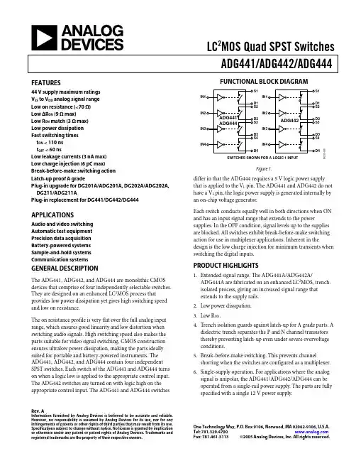
LC2MOS Quad SPST SwitchesADG441/ADG442/ADG444 Rev.AInformation furnished by Analog Devices is believed to be accurate and reliable.However, no responsibility is assumed by Analog Devices for its use, nor for anyinfringements of patents or other rights of third parties that may result from its use. Specifications subject to change without notice. No license is granted by implication or otherwise under any patent or patent rights of Analog Devices. Trademarks and registered trademarks are the property of their respective owners.One Technology Way, P.O. Box 9106, Norwood, MA 02062-9106, U.S.A. Tel: Fax: 781.461.3113©2005 Analog Devices, Inc. All rights reserved.FEATURES44 V supply maximum ratingsV SS to V DD analog signal rangeLow on resistance (<70 Ω)Low ∆R ON (9 Ω max)Low R ON match (3 Ω max)Low power dissipationFast switching timest ON < 110 nst OFF < 60 nsLow leakage currents (3 nA max)Low charge injection (6 pC max)Break-before-make switching actionLatch-up proof A gradePlug-in upgrade for DG201A/ADG201A, DG202A/ADG202A, DG211/ADG211APlug-in replacement for DG441/DG442/DG444APPLICATIONSAudio and video switchingAutomatic test equipmentPrecision data acquisitionBattery-powered systemsSample-and-hold systemsCommunication systemsGENERAL DESCRIPTIONThe ADG441, ADG442, and ADG444 are monolithic CMOS devices that comprise of four independently selectable switches. They are designed on an enhanced LC2MOS process that provides low power dissipation yet gives high switching speed and low on resistance.The on resistance profile is very flat over the full analog input range, which ensures good linearity and low distortion when switching audio signals. High switching speed also makes the parts suitable for video signal switching. CMOS construction ensures ultralow power dissipation, making the parts ideally suited for portable and battery-powered instruments. The ADG441, ADG442, and ADG444 contain four independent SPST switches. Each switch of the ADG441 and ADG444 turns on when a logic low is applied to the appropriate control input. The ADG442 switches are turned on with logic high on the appropriate control input. The ADG441 and ADG444 switchesFUNCTIONAL BLOCK DIAGRAM5233-1SWITCHES SHOWN FOR A LOGIC 1 INPUTFigure 1.differ in that the ADG444 requires a 5 V logic power supply that is applied to the V L pin. The ADG441 and ADG442 do not have a V L pin, the logic power supply is generated internally by an on-chip voltage generator.Each switch conducts equally well in both directions when ON and has an input signal range that extends to the power supplies. In the OFF condition, signal levels up to the supplies are blocked. All switches exhibit break-before-make switching action for use in multiplexer applications. Inherent in the design is the low charge injection for minimum transients when switching the digital inputs.PRODUCT HIGHLIGHTS1.Extended signal range. The ADG441A/ADG442A/ADG444A are fabricated on an enhanced LC2MOS, trench-isolated process, giving an increased signal range thatextends to the supply rails.2.Low power dissipation.3.Low R ON.4.Trench isolation guards against latch-up for A grade parts. Adielectric trench separates the P and N channel transistors thereby preventing latch-up even under severe overvoltage conditions.5.Break-before-make switching. This prevents channelshorting when the switches are configured as a multiplexer.6.Single-supply operation. For applications where the analogsignal is unipolar, the ADG441/ADG442/ADG444 can be operated from a single-rail power supply. The parts are fully specified with a single 12 V power supply.ADG441/ADG442/ADG444Rev. A | Page 2 of 16TABLE OF CONTENTSSpecifications.....................................................................................3 Dual Supply...................................................................................3 Single Supply.................................................................................4 Absolute Maximum Ratings............................................................5 ESD Caution..................................................................................5 Pin Configurations and Function Descriptions...........................6 Typical Performance Characteristics.............................................7 Test Circuits........................................................................................9 Terminology....................................................................................11 Trench Isolation..............................................................................12 Outline Dimensions.......................................................................13 Ordering Guide.. (14)REVISION HISTORY5/05—Data Sheet Changed from Rev. 0 to Rev. AChanges to Format.............................................................Universal Deleted CERDIP Package and T Grade ..........................Universal Changes to Features and Product Highlights...............................1 Changes to Test Conditions in Table 2..........................................4 Changes to Figure 11........................................................................8 Changes to Trench Isolation Section...........................................12 Updated Outline Dimensions.......................................................13 Changes to Ordering Guide..........................................................14 4/94–Revision 0: Initial VersionADG441/ADG442/ADG444Rev. A | Page 3 of 16SPECIFICATIONSDUAL SUPPLY 1V DD = +15 V ± 10%, V SS = −15 V ± 10%, V L = +5 V ± 10% (ADG444), GND = 0 V , unless otherwise noted. Table 1.B Version Parameter +25°C −40°C to +85°C Unit Test Conditions/Comments ANALOG SWITCH Analog Signal Range V SS to V DD V R ON 40 Ω typ V D = ±8.5 V, I S = −10 mA 70 85 Ω max V DD = +13.5 V, V SS = −13.5 V ∆R ON 4 Ω typ −8.5 V ≤ V D ≤ +8.5 V 9 Ω max R ON Match 1 Ω typ V D = 0 V, I S = −10 mA 3 Ω max LEAKAGE CURRENTS V DD = +16.5 V, V SS = −16.5 V Source OFF Leakage I S (OFF) ±0.01 nA typ V D = ±15.5 V, V S = ∓15.5 V±0.5 ±3 nA max See Figure 15Drain OFF Leakage I D (OFF) ±0.01nA typ V D = ±15.5 V, V S = ∓15.5 V±0.5 ±3 nA max See Figure 15 Channel ON Leakage I D , I S (ON) ±0.08 nA typ V S = V D = ±15.5 V±0.5 ±3 nA max See Figure 16 DIGITAL INPUTSInput High Voltage, V INH 2.4 V min Input Low Voltage, V INL 0.8 V max Input CurrentI INL or I INH ±0.00001 µA typ V IN = V INL or V INH±0.5 µA max DYNAMIC CHARACTERISTICS 2t ON 85 ns typ R L = 1 kΩ, C L = 35 pF; 110 170 ns max V S = ±10 V; see Figure 17 t OFF 45 ns typ R L = 1 kΩ, C L = 35 pF; 60 80 ns max V S = ±10 V; see Figure 17 t OPEN30 ns typ R L = 1 kΩ, C L = 35 pF;Charge Injection 1 pC typ V S = 0 V, R S = 0 Ω, C L = 1 nF;6 pC max V DD = +15 V, V SS = –15 V; see Figure 18OFF Isolation60 dB typ R L = 50 Ω, C L = 5 pF; f = 1 MHz; see Figure 19 Channel-to-Channel Crosstalk 100 dB typ R L = 50 Ω, C L = 5 pF; f= 1 MHz; see Figure 20 C S (OFF) 4 pF typ f = 1 MHz C D (OFF) 4 pF typ f = 1 MHz C D , C S (ON)16 pF typ f = 1 MHzPOWER REQUIREMENTS V DD = +16.5 V, V SS = −16.5 V I DDDigital Inputs = 0 V or 5 V ADG441/ADG44280 µA max ADG444 0.001 µA typ12.5 µA max I SS 0.0001 µA typ1 2.5 µA maxI L (ADG444 Only) 0.001 µA typ V L = 5.5 V12.5µA max1 Temperature range is: B Version: −40°C to +85°C.2Guaranteed by design, not subject to production test.ADG441/ADG442/ADG444SINGLE SUPPLY1V DD = +12 V ± 10%, V SS = 0 V, V L = +5 V ± 10% (ADG444), GND = 0 V, unless otherwise noted.Table 2.B VersionParameter +25°C −40°C to +85°C Unit Test Conditions/CommentsANALOG SWITCHAnalog Signal Range 0 to V DD VR ON70 Ω typ V D = +3 V, +8 V, I S = −5 mA110 130 Ω max V DD = 10.8 V∆R ON 4 Ω typ 3 V ≤ V D ≤ 8 V9 Ω maxR ON Match 1 Ω typ V D = +6 V, I S = −5 mA3 Ω maxLEAKAGE CURRENT V DD = 13.2 VSource OFF Leakage I S (OFF) ±0.01 nA typ V D = 12.2 V/1 V, V S = 1 V/12.2 V±0.5 ±3 nA max See Figure 15Drain OFF Leakage I D (OFF) ±0.01 nA typ V D = 12.2 V/1 V, V S = 1 V/12.2 V±0.5 ±3 nA max See Figure 15Channel ON Leakage I D, I S (ON) ±0.08 nA typ V S = V D = 12.2 V/1 V±0.5 ±3 nA max Figure 16DIGITAL INPUTSInput High Voltage, V INH 2.4 V minInput Low Voltage, V INL0.8 V maxInput CurrentI INL or I INH±0.00001 µA typ V IN = V INL or V INH±0.5 µA maxDYNAMIC CHARACTERISTICS2t ON105 ns typ R L = 1 kΩ, C L = 35 pF150 220 ns max V S = 8 V; Figure 17t OFF40 ns typ R L = 1 kΩ, C L = 35 pF60 100 ns max V S = 8 V; Figure 17t OPEN50 ns typ R L = 1 kΩ, C L = 35 pFCharge Injection 2 pC typ V S = 6 V, R S = 0 Ω, C L = 1 nF6 pC max V DD = 12 V, V SS = 0 V; see Figure 18OFF Isolation 60 dB typ R L = 50 Ω, C L = 5 pF, f = 1 MHz; see Figure 19 Channel-to-Channel Crosstalk 100 dB typ R L = 50 Ω, C L = 5 pF, f = 1 MHz; see Figure 20 C S (OFF) 7 pF typ f = 1 MHzC D (OFF) 10 pF typ f = 1 MHzC D, C S (ON) 16 pF typ f = 1 MHzPOWER REQUIREMENTS V DD = 13.2 VI DD Digital Inputs = 0 V or 5 VADG441/ADG442 80 µA maxADG444 0.001 µA typ1 2.5 µA maxI L (ADG444 Only) 0.001 µA typ V L = 5.5 V1 2.5 µA max1 Temperature range is: B Version: −40°C to +85°C.2 Guaranteed by design, not subject to production test.Rev. A | Page 4 of 16ADG441/ADG442/ADG444Rev. A | Page 5 of 16ABSOLUTE MAXIMUM RATINGST A = 25°C unless otherwise noted. Table 3.Parameter Rating V DD to V SS 44 V V DD to GND −0.3 V to +25 V V SS to GND +0.3 V to −25 V V L to GND −0.3 V to V DD + 0.3 V Analog, Digital Inputs V SS − 2 V to V DD + 2 V or 30 mA, Whichever Occurs First Continuous Current, S or D 30 mA Peak Current, S or D (Pulsed at 1 ms, 10% Duty Cycle Max) 100 mA Operating Temperature Range Industrial (B Version) −40°C to +85°C Storage Temperature Range −65°C to +150°C Junction Temperature 150°C Lead Temperature, Soldering (10 sec) 300°C Plastic Package, Power Dissipation 470 mW θJA , Thermal Impedance 177°C/W Lead Temperature, Soldering (10 sec) 260°C SOIC Package, Power Dissipation 600 mW θJA , Thermal Impedance 77°C/W Lead Temperature, Soldering Vapor Phase (60 sec) 215°C Infrared (15 sec) 220°CStresses above those listed under Absolute Maximum Ratings may cause permanent damage to the device. This is a stress rating only; functional operation of the device at these or any other conditions above those listed in the operational sections of this specification is not implied. Exposure to absolute maximum rating conditions for extended periods may affect device reliability. Only one absolute maximum rating may be applied at any one time.Table 4. Truth TableADG441/ADG444 IN ADG442 INSwitch Condition 0 1 ON 1OFFESD CAUTIONESD (electrostatic discharge) sensitive device. Electrostatic charges as high as 4000 V readily accumulateon the human body and test equipment and can discharge without detection. Although this product features proprietary ESD protection circuitry, permanent damage may occur on devices subjected to high energy electrostatic discharges. Therefore, proper ESD precautions are recommended to avoid performance degradation or loss of functionality.ADG441/ADG442/ADG444Rev. A | Page 6 of 16PIN CONFIGURATIONS AND FUNCTION DESCRIPTIONSV DDNC = NO CONNECT05233-002Figure 2. ADG441/ADG442 (DIP/SOIC)IN1D1S1V IN2D2S2V DD GND V LS4S3D4D3IN4IN305233-003Figure 3. ADG444 (DIP/SOIC)Table 5. ADG441/ADG442 Pin Function DescriptionsPin No. MnemonicDescription1, 8, 9, 16 IN1 to IN4 Logic Control Input. 2, 7, 10, 15D1 to D4Drain Terminal. May be an input or output.3, 6, 11, 14 S1 to S4 Source Terminal. May bean input or output.4 V SS Most Negative Power SupplyPotential in Dual Supplies. In single-supply applications, it may be connected to ground.5 GND Ground (0 V) Reference. 12 NC No Connect. 13 V DD Most Positive Power Supply Potential.Table 6. ADG444 Pin Function DescriptionsPin No. Mnemonic Description 1, 8, 9, 16 IN1 to IN4 Logic Control Input. 2, 7, 10, 15D1 to D4 Drain Terminal. May bean input or output.3, 6, 11, 14 S1 to S4 Source Terminal. May bean input or output.4 V SS Most Negative Power SupplyPotential in Dual Supplies. In single-supply applications, it may be connected to ground.5 GND Ground (0 V) Reference. 12 V L Logic Power Supply (5 V). 13 V DD Most Positive Power Supply Potential.ADG441/ADG442/ADG444Rev. A | Page 7 of 16TYPICAL PERFORMANCE CHARACTERISTICS05233-005V D (V S ) (V)15–15–10–5510R O N (Ω)10080604020Figure 4. R ON as a Function of V D (V S ): Dual Supply05233-006V D (V S ) (V)15036912R O N (Ω)1701101301507090503010Figure 5. R ON as a Function of V D (V S ): Single Supply05233-007V D (V S ) (V)15–15–10–5510R O N (Ω)10080604020V DD = +15V V SS =–15V125°C25°C85°CFigure 6. R ON as a Function of V D (V S ) for Different Temperatures 05233-008V S (V D ) (V)15–15–10–5510L E A K A G E C U R R EN T (n A )0.020.01–0.01–0.02Figure 7. Leakage Currents as a Function of V S (V D )05233-009FREQUENCY (Hz)10M1k10k100k1M d B1201001107080906050Figure 8. Crosstalk and Off Isolation vs. Frequency05233-010V D (V S ) (V)120246810R O N (Ω)12010060804020Figure 9. R ON as a Function of V D (V S ) for Different TemperaturesADG441/ADG442/ADG444Rev. A | Page 8 of 1605233-011V S , V D (V)120246810L E A K A G E C U R R E N T (n A )0.0100.0050–0.005–0.010Figure 10. Leakage Currents as a Function of V S (V D )05233-012V S (V)15–15–12–9–6–3036912C H A R G E I N J E C T I O N(p C )402010300–20–30–10–40Figure 11. Charge Injection vs. Source Voltage 05233-013SUPPLY VOLTAGE (V)±20±10±12±14±16±18V IN = 8Vt ONt OFFt (n s )120100806040Figure 12. Switching Time vs. Bipolar Supply05233-014SUPPLY VOLTAGE (V)2081014121618t (n s )16014012010080604020V IN = 8Vt ONt OFFFigure 13. Switching Time vs. Single SupplyADG441/ADG442/ADG444Rev. A | Page 9 of 16TEST CIRCUITSV S05233-015Figure 14. On ResistanceV SD05233-016Figure 15. Off LeakageV V D05233-017Figure 16. On LeakageV OUTV INV INV OUT05233-018Figure 17. Switching TimesV OUTV INV OUT05233-019Figure 18. Charge InjectionADG441/ADG442/ADG444Rev. A | Page 10 of 16V OUT05233-021Figure 19. Off IsolationV 05233-022CHANNEL-TO-CHANNEL CROSSTALK = 20×LOG |V S /V OUT |Figure 20. Channel-to-Channel CrosstalkTERMINOLOGYR ONOhmic resistance between D and S.R ON MatchDifference between the R ON of any two channels.I S (OFF)Source leakage current with the switch OFF.I D (OFF)Drain leakage current with the switch OFF.I D, I S (ON)Channel leakage current with the switch ON.V D (V S)Analog voltage on Terminals D, S.C S (OFF)OFF switch source capacitance.C D (OFF)OFF switch drain capacitance.C D, C S (ON)ON switch capacitance.t ONDelay between applying the digital control input and the outputswitching on.t OFFDelay between applying the digital control input and the outputswitching off.t OPENBreak-before-make delay when switches are configured as amultiplexer.CrosstalkA measure of unwanted signal which is coupled through fromone channel to another as a result of parasitic capacitance.Off IsolationA measure of unwanted signal coupling through an OFF switch.Charge InjectionA measure of the glitch impulse transferred from the digitalinput to the analog output during switching.Rev. A | Page 11 of 16Rev. A | Page 12 of 16TRENCH ISOLATIONIn the ADG441A, ADG442A, and ADG444A, an insulating oxide layer (trench) is placed between the NMOS and the PMOS transistors of each CMOS switch. Parasitic junctions, which occur between the transistors in junction isolatedswitches, are eliminated, and the result is a completely latch-up proof switch.In junction isolation, the N and P wells of the PMOS and NMOS transistors form a diode that is reverse-biased under normal operation. However, during overvoltage conditions, this diode becomes forward-biased. A silicon-controlled rectifier (SCR) type circuit is formed by the two transistors causing a significant amplification of the current which, in turn, leads to latch-up. With trench isolation, this diode is removed, and the result is a latch-up proof switch.05233-004LOCOFigure 21. Trench IsolationRev. A | Page 13 of 16OUTLINE DIMENSIONS0.150 (3.81)0.130 (3.30)0.110 (2.79)CONTROLLING DIMENSIONS ARE IN INCHES; MILLIMETER DIMENSIONS (IN PARENTHESES) ARE ROUNDED-OFF INCH EQUIVALENTS FORREFERENCE ONLY AND ARE NOT APPROPRIATE FOR USE IN DESIGNCOMPLIANT TO JEDEC STANDARDS MO-095ACFigure 22. 16-Lead Plastic Dual In-Line Package [PDIP](N-16)Dimensions shown in inches and (millimeters)CONTROLLING DIMENSIONS ARE IN MILLIMETERS; INCH DIMENSIONS (IN PARENTHESES) ARE ROUNDED-OFF MILLIMETER EQUIVALENTS FOR REFERENCE ONLY AND ARE NOT APPROPRIATE FOR USE IN DESIGNCOMPLIANT TO JEDEC STANDARDS MS-012AC45°Figure 23. 16-Lead Standard Small Outline Package [SOIC](R-16)Dimensions shown in millimeters and (inches)ORDERING GUIDEModel Temperature Range Package Description Package Option ADG441BN −40°C to +85°C 16-Lead Plastic Dual In-Line Package (PDIP) N-16ADG441BR −40°C to +85°C 16-Lead Standard Small Outline Package (SOIC) R-16ADG441BR-REEL −40°C to +85°C 16-Lead Standard Small Outline Package (SOIC) R-16ADG441BRZ1−40°C to +85°C 16-Lead Standard Small Outline Package (SOIC) R-16ADG441BRZ-REEL1−40°C to +85°C 16-Lead Standard Small Outline Package (SOIC) R-16ADG441BCHIPS DIEADG441ABCHIPS2 DIEADG441ABN2−40°C to +85°C 16-Lead Plastic Dual In-Line Package (PDIP) N-16ADG441ABR2−40°C to +85°C 16-Lead Standard Small Outline Package (SOIC) R-16ADG441ABR-REEL2−40°C to +85°C 16-Lead Standard Small Outline Package (SOIC) R-16ADG441ABRZ-REEL1, 2−40°C to +85°C 16-Lead Standard Small Outline Package (SOIC) R-16ADG442BN −40°C to +85°C 16-Lead Plastic Dual In-Line Package (PDIP) N-16ADG442BR −40°C to +85°C 16-Lead Standard Small Outline Package (SOIC) R-16ADG442BR-REEL −40°C to +85°C 16-Lead Standard Small Outline Package (SOIC) R-16ADG442BRZ1−40°C to +85°C 16-Lead Standard Small Outline Package (SOIC) R-16ADG442BRZ-REEL1−40°C to +85°C 16-Lead Standard Small Outline Package (SOIC) R-16ADG442ABN2−40°C to +85°C 16-Lead Plastic Dual In-Line Package (PDIP) N-16ADG442ABR2−40°C to +85°C 16-Lead Standard Small Outline Package (SOIC) R-16ADG442ABR-REEL2−40°C to +85°C 16-Lead Standard Small Outline Package (SOIC) R-16ADG442ABRZ1, 2−40°C to +85°C 16-Lead Standard Small Outline Package (SOIC) R-16ADG442ABRZ-REEL1, 2−40°C to +85°C 16-Lead Standard Small Outline Package (SOIC) R-16ADG444BN −40°C to +85°C 16-Lead Plastic Dual In-Line Package (PDIP) N-16ADG444BR −40°C to +85°C 16-Lead Standard Small Outline Package (SOIC) R-16ADG444BR-REEL −40°C to +85°C 16-Lead Standard Small Outline Package (SOIC) R-16ADG444BRZ1−40°C to +85°C 16-Lead Standard Small Outline Package (SOIC) R-16ADG444BRZ-REEL1−40°C to +85°C 16-Lead Standard Small Outline Package (SOIC) R-16ADG444ABN2−40°C to +85°C 16-Lead Plastic Dual In-Line Package (PDIP) N-16ADG444ABR2−40°C to +85°C 16-Lead Standard Small Outline Package (SOIC) R-16ADG444ABR-REEL2−40°C to +85°C 16-Lead Standard Small Outline Package (SOIC) R-16ADG444ABRZ1, 2−40°C to +85°C 16-Lead Standard Small Outline Package (SOIC) R-16ADG444ABRZ-REEL1, 2−40°C to +85°C 16-Lead Standard Small Outline Package (SOIC) R-161 Z = Pb-free part.2 A = Trench isolated.Rev. A | Page 14 of 16NOTESRev. A | Page 15 of 16NOTESregistered trademarks are the property of their respective owners.C00396–0–5/05(A)Rev. A | Page 16 of 16。