晶体管资料24c04(pdf 16)
- 格式:pdf
- 大小:125.15 KB
- 文档页数:16
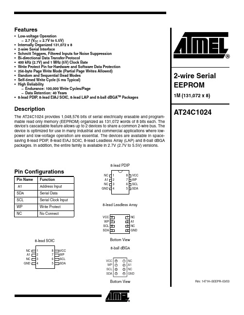
1Features•Low-voltage Operation –2.7 (V CC = 2.7V to 5.5V)•Internally Organized 131,072 x 8•2-wire Serial Interface•Schmitt Triggers, Filtered Inputs for Noise Suppression •Bi-directional Data Transfer Protocol•400 kHz (2.7V) and 1 MHz (5V) Clock Rate•Write Protect Pin for Hardware and Software Data Protection •256-byte Page Write Mode (Partial Page Writes Allowed)•Random and Sequential Read Modes •Self-timed Write Cycle (5 ms Typical)•High Reliability–Endurance: 100,000 Write Cycles/Page –Data Retention: 40 Years•8-lead PDIP , 8-lead EIAJ SOIC, 8-lead LAP and 8-ball dBGA TM PackagesDescriptionThe AT24C1024 provides 1,048,576 bits of serial electrically erasable and program-mable read only memory (EEPROM) organized as 131,072 words of 8 bits each. The device’s cascadable feature allows up to 2 devices to share a common 2-wire bus. The device is optimized for use in many industrial and commercial applications where low-power and low-voltage operation are essential. The devices are available in space-saving 8-lead PDIP, 8-lead EIAJ SOIC, 8-lead Leadless Array (LAP) and 8-ball dBGA packages. In addition, the entire family is available in 2.7V (2.7V to 5.5V) versions.Pin ConfigurationsPin Name Function A1Address Input SDA Serial Data SCL Serial Clock Input WPWrite Protect NCNo Connect8-lead PDIP8-lead Leadless ArrayBottom View8-lead SOIC8-ball dBGABottom View2AT24C10241471H–SEEPR–03/03Block DiagramAbsolute Maximum Ratings*Operating Temperature..................................-55°C to +125°C *NOTICE:Stresses beyond those listed under “Absolute Maximum Ratings” may cause permanent dam-age to the device. This is a stress rating only and functional operation of the device at these or any other conditions beyond those indicated in the operational sections of this specification is not implied. Exposure to absolute maximum rating conditions for extended periods may affect device reliability.Storage Temperature.....................................-65°C to +150°C Voltage on Any Pinwith Respect to Ground.....................................-1.0V to +7.0V Maximum Operating Voltage ..........................................6.25V DC Output Current........................................................5.0 mA3AT24C10241471H–SEEPR–03/03Pin DescriptionSERIAL CLOCK (SCL): The SCL input is used to positive edge clock data into each EEPROM device and negative edge clock data out of each device.SERIAL DATA (SDA): The SDA pin is bi-directional for serial data transfer. This pin is open-drain driven and may be wire-ORed with any number of other open-drain or open-collector devices.DEVICE/PAGE ADDRESSES (A1): The A1 pin is a device address input that can be hard-wired or left not connected for hardware compatibility with AT24C128/256/512. When the A1pin is hardwired, as many as two 1024K devices may be addressed on a single bus system (device addressing is discussed in detail under the Device Addressing section). When the pin is not hardwired, the default A1 is zero.WRITE PROTECT (WP): The hardware Write Protect pin is useful for protecting the entire contents of the memory from inadvertent write operations. The write-protect input, when tied to GND, allows normal write operations. When WP is tied high to V CC , all write operations to the memory are inhibited. If left unconnected, WP is internally pulled down to GND. Switching WP to V CC prior to a write operation creates a software write-protect function.Memory OrganizationAT24C1024, 1024K SERIAL EEPROM: The 1024K is internally organized as 512 pages of 256 bytes each. Random word addressing requires a 17-bit data word address.4AT24C10241471H–SEEPR–03/03Pin Capacitance (1)Note:1.This parameter is characterized and is not 100% tested.DC CharacteristicsNote:1.V IL min and V IH max are reference only and are not tested.Applicable over recommended operating range from T A = 25°C, f = 1.0 MHz, V CC = +2.7V.Symbol Test ConditionMax Units Conditions C I/O Input/Output Capacitance (SDA)8pF V I/O = 0V C IN Input Capacitance (A 1, SCL)6pFV IN = 0VApplicable over recommended operating range from: T AI = -40°C to +85°C, V CC = +2.7V to +5.5V, T AC = 0°C to +70°C,V CC = +2.7V to +5.5V (unless otherwise noted).Symbol Parameter Test ConditionMin TypMax Units V CC Supply Voltage 2.75.5V I CC Supply Current V CC = 5.0V READ at 400 kHz 2.0mA I CC Supply Current V CC = 5.0V WRITE at 400 kHz 5.0mA I SB Standby Current V CC = 2.7V V IN = V CC or V SS3.0µA V CC = 5.5V 6.0µA I LI Input Leakage Current V IN = V CC or V SS 0.10 3.0µA I LO Output Leakage CurrentV OUT = V CC or V SS0.053.0µA V IL Input Low Level (1)-0.6V CC x 0.3V V IH Input High Level (1)V CC x 0.7V CC + 0.5V V OL Output Low LevelV CC = 3.0VI OL = 2.1 mA0.4V5AT24C10241471H–SEEPR–03/03AC Characteristics2.AC measurement conditions:R L (connects to V CC ): 1.3 k Ω (2.7V , 5V)Input pulse voltages: 0.3 V CC to 0.7 V CC Input rise and fall times: ≤50 nsInput and output timing reference voltages: 0.5 V CCApplicable over recommended operating range from T A = -40°C to +85°C, V CC = +2.7V to +5.5V, C L = 100 pF (unless otherwise noted). Test conditions are listed in Note 2.Symbol ParameterTest Conditions MinMax Units f SCL Clock Frequency, SCL 4.5V ≤ V CC ≤ 5.5V 2.7V ≤ V CC ≤ 5.5V 1000400kHz t LOW Clock Pulse Width Low 4.5V ≤ V CC ≤ 5.5V 2.7V ≤ V CC ≤ 5.5V 0.41.3µs t HIGH Clock Pulse Width High 4.5V ≤ V CC ≤ 5.5V 2.7V ≤ V CC ≤ 5.5V 0.40.6µs t AA Clock Low to Data Out Valid4.5V ≤ V CC ≤5.5V 2.7V ≤ V CC ≤ 5.5V 0.050.050.550.9µs t BUF Time the bus must be free before a new transmission can start (1) 4.5V ≤ V CC ≤ 5.5V 2.7V ≤ V CC ≤ 5.5V 0.51.3µs t HD.STA Start Hold Time 4.5V ≤ V CC ≤ 5.5V 2.7V ≤ V CC ≤ 5.5V 0.250.6µs t SU.STA Start Setup Time 4.5V ≤ V CC ≤ 5.5V 2.7V ≤ V CC ≤ 5.5V0.250.6µs t HD.DAT Data In Hold Time 0µs t SU.DA T Data In Setup Time 100ns t R Inputs Rise Time (1)0.3µs t F Inputs Fall Time (1) 4.5V ≤ V CC ≤ 5.5V 2.7V ≤ V CC ≤ 5.5V 100300ns t SU.STO Stop Setup Time 4.5V ≤ V CC ≤ 5.5V 2.7V ≤ V CC ≤ 5.5V0.250.6µs t DH Data Out Hold Time 50ns t WRWrite Cycle Time10ms Endurance (1) 5.0V , 25°C, Page Mode100KWrite Cycles6AT24C10241471H–SEEPR–03/03Device OperationCLOCK and DATA TRANSITIONS: The SDA pin is normally pulled high with an external device. Data on the SDA pin may change only during SCL low time periods (refer to Data Validity timing diagram). Data changes during SCL high periods will indicate a start or stop condition as defined below.START CONDITION: A high-to-low transition of SDA with SCL high is a start condition which must precede any other command (refer to Start and Stop Definition timing diagram).STOP CONDITION: A low-to-high transition of SDA with SCL high is a stop condition. After a read sequence, the Stop command will place the EEPROM in a standby power mode (refer to Start and Stop Definition timing diagram).ACKNOWLEDGE: All addresses and data words are serially transmitted to and from the EEPROM in 8-bit words. The EEPROM sends a zero during the ninth clock cycle to acknowl-edge that it has received each word.STANDBY MODE: The AT24C1024 features a low-power standby mode which is enabled: a)upon power-up and b)after the receipt of the STOP bit and the completion of any internal operations.MEMORY RESET: After an interruption in protocol, power loss or system reset, any 2-wire part can be reset by following these steps:1.Clock up to 9 cycles,2.Look for SDA high in each cycle while SCL is high.3.Create a start condition.7AT24C10241471H–SEEPR–03/03Bus Timing (SCL: Serial Clock, SDA: Serial Data I/O)Write Cycle Timing (SCL: Serial Clock, SDA: Serial Data I/O)Note:1.The write cycle time t WRis the time from a valid stop condition of a write sequence to the end of the internal clear/write cycle.8AT24C10241471H–SEEPR–03/03Data ValidityStart and Stop DefinitionOutput Acknowledge9AT24C10241471H–SEEPR–03/03DeviceAddressingThe 1024K EEPROM requires an 8-bit device address word following a start condition to enable the chip for a read or write operation (refer to Figure 1). The device address word con-sists of a mandatory one, zero sequence for the first five most significant bits as shown. This is common to all 2-wire EEPROM devices.The 1024K uses the one device address bit, A1, to allow up to two devices on the same bus.The A1 bit must compare to the corresponding hardwired input pin. The A1 pin uses an inter-nal proprietary circuit that biases it to a logic low condition if the pin is allowed to float.The seventh bit (P 0) of the device address is a memory page address bit. This memory page address bit is the most significant bit of the data word address that follows. The eighth bit of the device address is the read/write operation select bit. A read operation is initiated if this bit is high and a write operation is initiated if this bit is low.Upon a compare of the device address, the EEPROM will output a zero. If a compare is not made, the device will return to a standby state.DATA SECURITY: The AT24C1024 has a hardware data protection scheme that allows the user to write-protect the entire memory when the WP pin is at V CC .WriteOperationsBYTE WRITE: To select a data word in the 1024K memory requires a 17-bit word address.The word address field consists of the P 0 bit of the device address, then the most significant word address followed by the least significant word address (refer to Figure 2)A write operation requires the P 0 bit and two 8-bit data word addresses following the device address word and acknowledgment. Upon receipt of this address, the EEPROM will again respond with a zero and then clock in the first 8-bit data word. Following receipt of the 8-bit data word, the EEPROM will output a zero. The addressing device, such as a microcontroller,then must terminate the write sequence with a stop condition. At this time the EEPROM enters an internally timed write cycle, T WR , to the nonvolatile memory. All inputs are disabled during this write cycle and the EEPROM will not respond until the write is complete (refer to Figure 2).PAGE WRITE: The 1024K EEPROM is capable of 256-byte page writes.A page write is initiated the same way as a byte write, but the microcontroller does not send a stop condition after the first data word is clocked in. Instead, after the EEPROM acknowledges receipt of the first data word, the microcontroller can transmit up to 255 more data words. The EEPROM will respond with a zero after each data word received. The microcontroller must ter-minate the page write sequence with a stop condition (refer to Figure 3).The data word address lower 8 bits are internally incremented following the receipt of each data word. The higher data word address bits are not incremented, retaining the memory page row location. When the word address, internally generated, reaches the page boundary, the following byte is placed at the beginning of the same page. If more than 256 data words are transmitted to the EEPROM, the data word address will “roll over” and previous data will be overwritten. The address “rollover” during write is from the last byte of the current page to the first byte of the same page.ACKNOWLEDGE POLLING: Once the internally timed write cycle has started and the EEPROM inputs are disabled, acknowledge polling can be initiated. This involves sending a start condition followed by the device address word. The read/write bit is representative of the operation desired. Only if the internal write cycle has completed will the EEPROM respond with a zero, allowing the read or write sequence to continue.10AT24C10241471H–SEEPR–03/03ReadOperationsRead operations are initiated the same way as write operations with the exception that the read/write select bit in the device address word is set to one. There are three read operations:current address read, random address read and sequential read.CURRENT ADDRESS READ: The internal data word address counter maintains the last address accessed during the last read or write operation, incremented by one. This address stays valid between operations as long as the chip power is maintained. The address “rollover”during read is from the last byte of the last memory page, to the first byte of the first page.Once the device address with the read/write select bit set to one is clocked in and acknowl-edged by the EEPROM, the current address data word is serially clocked out. The microcontroller does not respond with an input zero but does generate a following stop condi-tion (refer to Figure 4).RANDOM READ: A random read requires a “dummy” byte write sequence to load in the data word address. Once the device address word and data word address are clocked in and acknowledged by the EEPROM, the microcontroller must generate another start condition.The microcontroller now initiates a current address read by sending a device address with the read/write select bit high. The EEPROM acknowledges the device address and serially clocks out the data word. The microcontroller does not respond with a zero but does generate a fol-lowing stop condition (refer to Figure 5).SEQUENTIAL READ: Sequential reads are initiated by either a current address read or a ran-dom address read. After the microcontroller receives a data word, it responds with an acknowledge. As long as the EEPROM receives an acknowledge, it will continue to increment the data word address and serially clock out sequential data words. When the memory address limit is reached, the data word address will “roll over” and the sequential read will con-tinue. The sequential read operation is terminated when the microcontroller does not respond with a zero, but does generate a following stop condition (refer to Figure 6).11AT24C10241471H–SEEPR–03/03Figure 1. Device AddressFigure 2. Byte WriteFigure 3. Page WriteFigure 4.Current Address Read12AT24C10241471H–SEEPR–03/03Figure 5. Random ReadFigure 6.Sequential Read13AT24C10241471H–SEEPR–03/03Note:For 2.7V devices used in the 4.5V to 5.5V range, please refer to performance values in the AC and DC Characteristics tables.Ordering InformationOrdering CodePackage Operation RangeA T24C1024-10CI-2.7A T24C1024C1-10CI-2.7A T24C1024-10PI-2.7A T24C1024W-10SI-2.7A T24C1024-10UI-2.78CN38CN18P38S28U8Industrial (-40°C to 85°C)Package Type8CN38-lead, 0.230" Wide, Leadless Array Package (LAP)8CN18-lead, 0.300" Wide, Leadless Array Package (LAP)8P38-lead, 0.300" Wide, Plastic Dual In-line Package (PDIP)8S28-lead, 0.200" Wide, Plastic Gull Wing Small Outline Package (EIAJ SOIC)8U88-ball, die Ball Grid Array Package (dBGA)Options-2.7Low Voltage (2.7V to 5.5V)14AT24C10241471H–SEEPR–03/03Packaging Information8CN3 – LAP15AT24C10241471H–SEEPR–03/038CN1 – LAP16AT24C10241471H–SEEPR–03/038P3 – PDIP17AT24C10241471H–SEEPR–03/038S2 – EIAJ SOIC18AT24C10241471H–SEEPR–03/038U8 – dBGA1471H–SEEPR–03/03xMDisclaimer: Atmel Corporation makes no warranty for the use of its products, other than those expressly contained in the Company’s standard warranty which is detailed in Atmel’s Terms and Conditions located on the Company’s web site. The Company assumes no responsibility for any errors which may appear in this document, reserves the right to change devices or specifications detailed herein at any time without notice, and does not make any commitment to update the information contained herein. No licenses to patents or other intellectual property of Atmel are granted by the Company in connection with the sale of Atmel products, expressly or by implication. Atmel’s products are not authorized for use as critical components in life support devices or systems.Atmel CorporationAtmel Operations2325 Orchard Parkway San Jose, CA 95131Tel: 1(408) 441-0311Fax: 1(408) 487-2600Regional HeadquartersEuropeAtmel SarlRoute des Arsenaux 41Case Postale 80CH-1705 Fribourg SwitzerlandTel: (41) 26-426-5555Fax: (41) 26-426-5500AsiaRoom 1219Chinachem Golden Plaza 77 Mody Road Tsimshatsui East Kowloon Hong KongTel: (852) 2721-9778Fax: (852) 2722-1369Japan9F, Tonetsu Shinkawa Bldg.1-24-8 ShinkawaChuo-ku, Tokyo 104-0033JapanTel: (81) 3-3523-3551Fax: (81) 3-3523-7581Memory2325 Orchard Parkway San Jose, CA 95131Tel: 1(408) 441-0311Fax: 1(408) 436-4314Microcontrollers2325 Orchard Parkway San Jose, CA 95131Tel: 1(408) 441-0311Fax: 1(408) 436-4314La Chantrerie BP 7060244306 Nantes Cedex 3, France Tel: (33) 2-40-18-18-18Fax: (33) 2-40-18-19-60ASIC/ASSP/Smart CardsZone Industrielle13106 Rousset Cedex, France Tel: (33) 4-42-53-60-00Fax: (33) 4-42-53-60-011150 East Cheyenne Mtn. Blvd.Colorado Springs, CO 80906Tel: 1(719) 576-3300Fax: 1(719) 540-1759Scottish Enterprise Technology Park Maxwell BuildingEast Kilbride G75 0QR, Scotland Tel: (44) 1355-803-000Fax: (44) 1355-242-743RF/AutomotiveTheresienstrasse 2Postfach 353574025 Heilbronn, Germany Tel: (49) 71-31-67-0Fax: (49) 71-31-67-23401150 East Cheyenne Mtn. Blvd.Colorado Springs, CO 80906Tel: 1(719) 576-3300Fax: 1(719) 540-1759Biometrics/Imaging/Hi-Rel MPU/High Speed Converters/RF DatacomAvenue de Rochepleine BP 12338521 Saint-Egreve Cedex, France Tel: (33) 4-76-58-30-00Fax: (33) 4-76-58-34-80e-mailliterature@Web Site© Atmel Corporation 2003. All rights reserved. Atmel ® and combinations thereof, are the registered trademarks, and dBG A ™ is the trademark of Atmel Corporation or its subsidiaries. Other terms and product names may be the trademarks of others.。

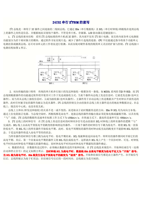
24C02串行E2PROM的读写I2C总线是一种用于IC器件之间连接的二线制总线。
它通过SDA(串行数据线)及SCL(串行时钟线)两根线在连到总线上的器件之间传送信息,并根据地址识别每个器件:不管是单片机、存储器、LCD驱动器还是键盘接口。
1.I2C总线的基本结构采用I2C总线标准的单片机或IC器件,其内部不仅有I2C接口电路,而且将内部各单元电路按功能划分为若干相对独立的模块,通过软件寻址实现片选,减少了器件片选线的连接。
CPU不仅能通过指令将某个功能单元电路挂靠或摘离总线,还可对该单元的工作状况进行检测,从而实现对硬件系统的既简单又灵活的扩展与控制。
I2C总线接口电路结构如图1所示。
2.双向传输的接口特性传统的单片机串行接口的发送和接收一般都各用一条线,如MCS51系列的TXD和RXD,而I2C 总线则根据器件的功能通过软件程序使其可工作于发送或接收方式。
当某个器件向总线上发送信息时,它就是发送器(也叫主器件),而当其从总线上接收信息时,又成为接收器(也叫从器件)。
主器件用于启动总线上传送数据并产生时钟以开放传送的器件,此时任何被寻址的器件均被认为是从器件。
I2C总线的控制完全由挂接在总线上的主器件送出的地址和数据决定。
在总线上,既没有中心机,也没有优先机。
总线上主和从(即发送和接收)的关系不是一成不变的,而是取决于此时数据传送的方向。
SDA和SCL均为双向I/O线,通过上拉电阻接正电源。
当总线空闲时,两根线都是高电平。
连接总线的器件的输出级必须是集电极或漏极开路,以具有线“与”功能。
I2C总线的数据传送速率在标准工作方式下为100kbit/s,在快速方式下,最高传送速率可达400kbit/s。
3.I2C总线上的时钟信号在I2C总线上传送信息时的时钟同步信号是由挂接在SCL时钟线上的所有器件的逻辑“与”完成的。
SCL线上由高电平到低电平的跳变将影响到这些器件,一旦某个器件的时钟信号下跳为低电平,将使SCL线一直保持低电平,使SCL线上的所有器件开始低电平期。
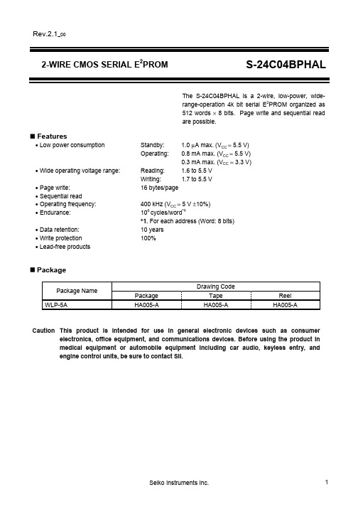
Rev.2.1_002-WIRE CMOS SERIAL E2PROM S-24C04BPHALThe S-24C04BPHAL is a 2-wire, low-power, wide-range-operation 4k bit serial E2PROM organized as512 words × 8 bits. Page write and sequential readare possible.Features• Low power consumption Standby: 1.0 µA max. (V CC = 5.5 V)Operating: 0.8 mA max. (V CC = 5.5 V)0.3 mA max. (V CC= 3.3 V)• Wide operating voltage range: Reading: 1.6 to 5.5 VWriting: 1.7 to 5.5 V• Page write: 16 bytes/page• Sequential read• Operating frequency: 400 kHz (V CC = 5 V ±10%)• Endurance: 106 cycles/word*1*1. For each address (Word: 8 bits)• Data retention: 10 years• Write protection 100%• Lead-free productsPackageDrawing CodePackage NamePackage Tape Reel WLP-5A HA005-A HA005-A HA005-ACaution This product is intended for use in general electronic devices such as consumer electronics, office equipment, and communications devices. Before using the product inmedical equipment or automobile equipment including car audio, keyless entry, andengine control units, be sure to contact SII.2-WIRE CMOS SERIAL E 2PROMS-24C04BPHAL Rev.2.1_00Pin ConfigurationWLP-5A Bottom viewTable 1Pin No. Symbol Description 1 VCC Power supply 2SDASerial data I/O3 WP Write Protection pinConnected to Vcc: Protection validConnected to GND: Protection invalid4 SCL Serial clock input5 GND GroundRemark See Dimensions for details of the package drawings. Figure 1S-24C04BPHAL2-WIRE CMOS SERIAL E2PROM Rev.2.1_00S-24C04BPHALBlock DiagramSCLSDAFigure 2Absolute Maximum RatingsTable 2UnitItem SymbolRatingsPower supply voltage V CC −0.3 to +7.0 VInput voltage V IN −0.3 to V CC+ 0.3 VOutput voltage V OUT −0.3 to V CC VOperating ambient temperature T opr−40 to + 85 °CStorage temperature T stg −65 to + 150 °CCaution The absolute maximum ratings are rated values exceeding which theproduct could suffer physical damage. These values must thereforenot be exceeded under any condition.2-WIRE CMOS SERIAL E2PROMS-24C04BPHAL Rev.2.1_00Recommended Operating ConditionsTable 3Max.Typ.UnitMin.Item SymbolConditionsReading 1.6− 5.5 V Power supply voltage V CCWriting 1.7− 5.5 VV CC = 2.5 to 5.5 V 0.7 × V CC−V CC V High-level input voltage V IHV CC = 1.6 to 2.5 V 0.8 × V CC−V CC VV CC = 2.5 to 5.5 V 0.0 −0.3 × V CC V Low-level input voltage V ILV CC = 1.6 to 2.5 V 0.0 −0.2 × V CC VPin CapacitanceTable 4(Ta = 25°C, f = 1.0 MHz, Vcc = 5 V)Max.Typ.UnitMin.Item SymbolConditionsInput capacitance C IN V IN= 0 V (SCL, WP) −−10 pFInput/output capacitance C I/O V I/O = 0 V (SDA) −−10 pFEnduranceTable 5Operating Temperature Min. Typ. Max. Unit Item SymbolEndurance NW −40 to +85°C 106 −−Cycles/word*1 *1. For each address (Word: 8 bits)2-WIRE CMOS SERIAL E 2PROMRev.2.1_00S-24C04BPHALDC Electrical CharacteristicsTable 6V CC = 4.5 to 5.5 V V CC = 2.5 to 4.5 V V CC = 1.6 to 2.5 VItem Symbol Conditions Min.Typ.Max.Min.Typ.Max. Min. Typ. Max.UnitCurrent consumption (READ)I CC1 f = 100 kHz − − 0.8*1− − 0.3 − − 0.2 mA Current consumption (PROGRAM) I CC2 f = 100 kHz − − 4.0 − − 1.5 − − 1.5*2mA *1. f = 400 kHz*2. V CC = 1.7 to 2.5 VTable 7V CC = 4.5 to 5.5 V V CC = 2.5 to 4.5 V V CC = 1.6 to 2.5 V Item Symbol ConditionsMin.Typ.Max.Min.Typ.Max. Min. Typ. Max.Unit Standby currentconsumptionI SB V IN = V CC or GND − − 1.0 − − 0.6 − − 0.4 µA Input currentleakageI LI V IN = GND to V CC −0.1 1.0 − 0.1 1.0 − 0.1 1.0 µA Output currentleakageI LO V OUT = GND to V CC −0.1 1.0 − 0.1 1.0 − 0.1 1.0 µA I OL = 3.2 mA − − 0.4 − − 0.4 − − − V Low-level output voltage V OL I OL = 1.5 mA − − 0.3 − − 0.3 − − 0.5 V Current addresshold voltageV AH − 1.5 − 5.5 1.5 − 4.5 1.5 − 2.5 V2-WIRE CMOS SERIAL E 2PROMS-24C04BPHALRev.2.1_00AC Electrical CharacteristicsTable 8 Measurement ConditionsInput pulse voltage 0.1 × V CC to 0.9 × V CC Input pulse rise/fall time 20 ns Output judgment voltage 0.5 × V CC Output load 100 pF + pull-up resistor 1.0 k Ω= 100 pFCC= 1.0 k ΩFigure 3 Output Load CircuitTable 9V CC = 4.5 to 5.5 V V CC = 1.6 to 4.5 VItem Symbol Min. Typ. Max. Min. Typ. Max.UnitSCL clock frequency f SCL 0 − 400 0 − 100 kHz SCL clock time “L” t LOW 1.0 − − 4.7 − − µs SCL clock time “H” t HIGH 0.9 − − 4.0 − − µs SDA output delay time t AA 0.1 − 0.9 0.1 −3.5 µs SDA output hold time t DH 50 − − 100 − − ns Start condition setup time t SU. STA 0.6 − −4.7 − − µs Start condition hold time t HD. STA 0.6 − − 4.0 − − µs Data input setup time t SU. DAT 100 − − 200 − − ns Data input hold time t HD. DAT 0 − − 0 − − ns Stop condition setup time t SU. STO 0.6 − − 4.7 − − µs SCL • SDA rise time t R − − 0.3 − − 1.0 µs SCL • SDA fall time t F − − 0.3 − − 0.3 µs Bus release time t BUF 1.3 − − 4.7 −−µsNoise suppression timet I− −50−−100 nsSCLSDA INSDA OUTFigure 4 Bus Timing2-WIRE CMOS SERIAL E2PROM Rev.2.1_00S-24C04BPHALTable 10Item Symbol Min. Typ. Max. UnitWrite time t WR 4.0 10.0 msSCLSDAAcknowledgeFigure 5 Write Cycle Timing2-WIRE CMOS SERIAL E2PROMS-24C04BPHAL Rev.2.1_00Pin Functions1. SDA (serial data input/output) pinThe SDA pin is used for bidirectional transfer of serial data. It consists of a signal input pin and an Nch open-drain transistor output pin. Usually pull up the SDA line to V CC via a resistor, and use it with other open-drain or open-collector output devices connected in a wired-OR configuration.2. SCL (serial clock input) pinThe SCL pin is used for serial clock input. It is capable of processing signals at the rising and falling edges of the SCL clock input signal. Make sure the rise time and fall time conform to the specifications.3. WP pinThe WP pin is used for write protection. When there is no need for write protection, connect the pin to GND; when there is a need for write protection, connect the pin to V CC.2-WIRE CMOS SERIAL E2PROM Rev.2.1_00S-24C04BPHAL Operation1. Start conditionWhen the SDA line changes from “H” to “L” with the SCL line at “H”, the device is in the start condition.All operations begin from the start condition.2. Stop conditionWhen the SDA line changes from “L” to “H” with the SCL line at “H”, the device is in the stop condition.When the device receives the stop condition signal during a read sequence, the read operation is interrupted, and the device enters standby mode.When the device receives the stop condition signal during a write sequence, the retrieval of write data is halted, and rewriting the E2PROM starts.t SU. STOt SU. STA t HD. STAStart condition Stop conditionFigure 6 Start/Stop Condition2-WIRE CMOS SERIAL E2PROMS-24C04BPHAL Rev.2.1_003. Data transferChanging the SDA line while the SCL line is “L” allows the data to be transferred.A start or stop condition is recognized when the SDA line changes while the SCL line is “H”.SCLSDAFigure 7 Data Transfer Timing4. Acknowledgment8 bits of data are transferred in succession. The device on the system bus that receives the data changesthe SDA line to “L” during the 9th clock cycle and outputs the acknowledge signal to inform that it has received the data.The device does not output the acknowledge signal while the E2PROM is being rewritten.SCL(E2SDASDA(E2Figure 8 Acknowledge Output Timing5. Device addressingTo perform data communications, the master device mounted on the system outputs the start condition signal to the slave device. Next, the master device outputs a 7-bit device address and a 1-bit read/write instruction code onto the SDA bus.The higher 4 bits of the device address are called the “Device Code”, and are fixed to “1010”. The following 2 bits are “don’t care” bits.When the comparison results match, the slave device outputs the acknowledge signal during the 9th clock cycle.Device codeS-24C04BPHALMSBLSBDon’t care Remark X: Don’t careFigure 9 Device AddressIn the S-24C04BPHAL, the 7th bit is a page address bit.Accordingly, when P0 = 0, the first half of the memory area (2 Kb: addresses 000h to 0FFh) is selected; when P0 = 1, the second half of the memory area (2 Kb; addresses 100h to 1FFh) are selected.6. Write operation6.1 Byte writeWhen the E 2PROM receives a 7-bit device address and the 1-bit read/write instruction code “0”, following the start condition signal, it outputs the acknowledge signal.Next, when the E 2PROM receives an 8-bit word address, it outputs the acknowledge signal.After the E 2PROM receives 8-bit write data and outputs the acknowledge signal, it receives the stop condition signal. Next, rewriting the specified memory address of the E 2PROM starts.While the E 2PROM is being rewritten, all operations are prohibited and the acknowledge signal is not output.S T A W R I M S B SDA lineADR INC(ADDRESS INCREMENT)A C K S T A C KA C KFigure 10 Byte Write6.2 Page writeUp to 16 bytes per page can be written in the S-24C04BPHAL.Basic data transfer procedures are the same as those in “Byte write”. The S-24C04BPHAL performs page write by successively receiving 8-bit write data sized pages.When the E2PROM receives a 7-bit device address and the 1-bit read/write instruction code “0” following the start condition signal, it outputs the acknowledge signal. When the E2PROM receives an 8-bit word address, it outputs the acknowledge signal. After the E2PROM receives 8-bit write data and outputs the acknowledge signal, it receives 8-bit write data corresponding to the next word address, and outputs the acknowledge signal. The E2PROM repeats reception of 8-bit write data and output of the acknowledge signal in succession and can receive write data corresponding to the maximum page size. When the stop condition signal is received, E2PROM corresponding to the size of the page on which write data starting from the specified memory address is received starts to be rewritten.S WFigure 11 Page WriteThe lower 4 bits of the word address are automatically incremented each time when the E2PROM receives 8-bit write data. Even when the write data exceeds 16 bytes, the higher 4 bits of the word address and page address P0 remain unchanged, and the lower 4 bits are rolled over and overwritten.6.3 Write ProtectionWrite protection is available in the S-24C04BPHAL. When the WP pin is connected to the V CC , write operation to memory area is forbidden at all.When the WP pin is connected to the GND, the write protection is invalid, and write operation in all memory area is available.Fix the level of the WP pin from the rising edge of SCL for loading the last write data (D0) until the end of the write time (10 ms max.). If the WP pin changes during this time, the address data being written at this time is not guaranteed.There is no need for using write protection, the WP pin should be connected to the GND. The write protection is valid in the operating voltage range.SDAWPSCLFigure 12 WP Pin Fixed Period6.4 Acknowledge PollingAcknowledge polling is used to know the completion of the write cycle in the E 2PROM.After the E 2PROM receives a stop condition and once starts the write cycle, all operations are forbidden and no response is made to the signal transmitted by the master device.Accordingly the master device can recognize the completion of the write cycle in the E 2PROM by detecting a response from the slave device after transmitting the start condition, the device address and the read/write instruction code to the E 2PROM, namely to the slave devices.That is, if the E 2PROM does not generate an acknowledge, the write cycle is in progress and if the E 2PROM generates an acknowledge, the write cycle has been completed. Keep the level of the WP pin fixed until acknowledge is confirmed.It is recommended to use the read instruction "1" as the read/write instruction code transmitted by the master device.7. Read7.1 Current address readThe E 2PROM holds the last accessed memory address during both writing and reading. The memory address is retained as long as the power voltage is the retention voltage V AH or more. Accordingly, when the master device recognizes the position of the address pointer inside the E 2PROM, data can be read from the memory address of the current address pointer without specifying a word address. This is called “Current Address Read”.“Current Address Read” is explained for when the address counter inside the E 2PROM is address “n”.When the E 2PROM receives a 7-bit device address and the 1-bit read/write instruction code “1”, following the start condition signal, it outputs the acknowledge signal.Next, 8-bit data at address “n” is output from the E 2PROM, in synchronization with the SCL clock.The address counter is incremented to address n + 1 at the falling edge of the SCL clock at which the 8th bit of data is output. The master device does not output the acknowledge signal and transmits the stop condition signal to finish reading.M S BDATAFigure 13 Current Address ReadFor recognition of the address pointer inside the E 2PROM, take into consideration the following:The memory address counter inside the E 2PROM is automatically incremented for every falling edge of the SCL clock at which the 8th bit of data is output during reading. During writing, the higher bits of the memory address (higher 4 bits of the word address) are left unchanged and are not incremented at any falling of the SCL clock when the 8th bit of the write data is received.7.2 Random readRandom read is a mode used when data is read from arbitrary memory addresses.To load a memory address into the address counter inside the E2PROM, first perform a dummy write following the procedure below.When the E2PROM receives a 7-bit device address and the 1-bit read/write instruction code “0” following the start condition signal, it outputs the acknowledge signal.Next, the E2PROM receives an 8-bit word address and outputs the acknowledge signal. The memory address has now been loaded into the address counter of the E2PROM.Following this, the E2PROM receives the write data during byte or page writing. However, data reception is not performed during dummy write.The memory address is loaded into the memory address counter inside the E2PROM during dummy write.After that, the master device can read the data starting from the arbitrary memory address by transmitting a new start condition signal and performing the same operation as that in the “Current Address Read”.That is, when the E2PROM receives a 7-bit device address and the 1-bit read/write instruction code “1”following the start condition signal, it outputs the acknowledge signal.Next, 8-bit data is output from the E2PROM in synchronization with the SCL clock. The master device does not output an acknowledge signal and transmits the stop condition signal instead. Reading is then complete.Figure 14 Random Read7.3 Sequential readWhen the E2PROM receives a 7-bit device address and the 1-bit read/write instruction code “1” in both current and random read operations following the start condition signal, it outputs the acknowledge signal.When 8-bit data is output from the E2PROM, in synchronization with the SCL clock, the memory address counter inside the E2PROM is automatically incremented at the falling edge of the SCL clock at which the 8th data is output.When the master device transmits the acknowledge signal, the next memory address data is output.When the master device transmits the acknowledge signal, the memory address counter inside the E2PROM is incremented and data can be read in succession. This is called “Sequential Read”.When the master device does not output an acknowledge signal and transmits the stop condition signal, the read operation is finished.Data can be read in the “Sequential Read” mode in succession. When the memory address counter reaches the last word address, it rolls over to the first memory address.SDAlineFigure 15 Sequential Read8. Address increment timingThe address increment timing is as follows. During a read operation, the memory address counter is automatically incremented at the falling edge of the SCL clock (where the 8th bit of read data is output).During a write operation, the memory address counter is also automatically incremented at the falling edge of the SCL clock when the 8th bit of write data is fetched.SDAAddress incrementFigure 16 Address Increment Timing in Read OperationSCLAddress incrementFigure 17 Address Increment Timing in Write OperationUsing S-24C04BPHAL1. Adding a pull-up resistor to SDA I/O pin and SCL input pinAdd a 1 k Ω to 5 k Ω pull-up resistor to the SCL input pin *1 and the SDA I/O pin in order to enable the functions of the I 2C Bus protocol. Normal communication cannot be provided without a pull-up resistor.*1. When the SCL input pin of the E 2PROM is connected to a tri-state output pin of the microprocessor,connect the same pull-up resistor to prevent a high impedance status from being input to the SCL input pin.This protects the E 2PROM from malfunction due to an undefined output (high impedance) from the tri-state pin when the microprocessor is reset when the voltage drops.2. Slave addressThe S-24C04BPHAL does not have slave address pins (A0, A1, A2). Therefore two or more of this IC cannot be used on the same bus.However, slave addresses can be used without changing the communication software because they are arbitrary addresses in communication with the master device.SDA lineMSBLSBFigure 183. I/O pin equivalent circuitThe I/O pins of this IC do not include pull-up and pull-down resistors. The SDA pin is an open-drain output.The following shows the equivalent circuits.Figure 19 SCL PinFigure 20 WP PinFigure 21 SDA Pin4. Maximum effectiveness of write protectionThe following conditions must be satisfied to prevent erroneous writing at power-on due to write protection.(1) Set the WP pin to high level at a time other than when the write instruction is being executed, includingduring power-on or off.(2) Adjust the phase after power-on.Pulling up the WP pin to V CC to always enable the WP pin at the absolute maximum rated voltage or lower prohibits writing all the time regardless of the conditions of the VCC, SDA, and SCL pins.5. Matching phases while E2PROM is accessedThe S-24C04BPHAL does not have a pin for resetting (the internal circuit), therefore, the E2PROM cannot be forcibly reset externally. If a communication interruption occurs in the E2PROM, it must be reset by software.For example, even if a reset signal is input to the microprocessor, the internal circuit of the E2PROM is not reset as long as the stop condition is not input to the E2PROM. In other words, the E2PROM retains the same status and cannot shift to the next operation. This symptom applies to the case when only the microprocessor is reset when the power supply voltage drops. With this status, if the power supply voltage is restored, reset the E2PROM (after matching the phase with the microprocessor) and input an instruction.The following shows this reset method.[How to reset E2PROM]The E2PROM can be reset by the start and stop instructions. When the E2PROM is reading data “0” or is outputting the acknowledge signal, 0 is output to the SDA line. In this status, the microprocessor cannot output an instruction to the SDA line. In this case, terminate the acknowledge output operation or read operation, and then input a start instruction. Figure 22 shows this procedure.First, input the condition. Then transmit 9 clocks (dummy clocks) of SCL. During this time, the microprocessor sets the SDA line to high level. By this operation, the E2PROM interrupts the acknowledge output operation or data output, so input the start condition*1. When a start condition is input, the E2PROM is reset. To make doubly sure, input the stop condition to the E2PROM. Normal operation is then possible.Figure 22 Resetting E2PROM*1. After 9 clocks (dummy clocks), if the SCL clock continues to be output without a start condition being input, a write operation may be started upon receipt of a stop condition. To prevent this, inputa start condition after 9 clocks (dummy clocks).Remark It is recommended to perform the above reset using dummy clocks when the system is initialized after the power supply voltage has been raised.6. Acknowledge checkThe I2C Bus protocol includes an acknowledge check function as a handshake function to prevent a communication error. This function allows detection of a communication failure during data communication between the microprocessor and E2PROM. This function is effective to prevent malfunction, so it is recommended to perform an acknowledge check on the microprocessor side.7. Built-in power-on-clear circuitE2PROMs have a built-in power-on-clear circuit that initializes the E2PROM. Unsuccessful initialization may cause a malfunction. For the power-on-clear circuit to operate normally, the following conditions must be satisfied for raising the power supply voltage.7.1 Raising power supply voltageRaise the power supply voltage, starting at 0.2 V maximum, so that the voltage reaches the power supply voltage to be used within the time defined by t RISE as shown in Figure 23.For example, when the power supply voltage to be used is 5.0 V, t RISE is 200 ms as shown in Figure 24.The power supply voltage must be raised within 200 ms.V INIT (Max.) Power supply voltage (V CC) 0 V*1*1. 0 V means there is no difference in potential between the V CC pin and the GND pin of the E2PROM.*2. t INIT is the time required to initialize the E2PROM. No instructions are accepted during this time.Figure 23 Raising Power Supply VoltageRise time (t RISE ) Max.[ms]Power supply voltage(V CC ) [V]505.04.03.02.0100150 200 For example:If your E 2PROM supply voltage = 5.0 V, raise the power supply voltage to 5.0 V within 200 ms.Figure 24 Raising Time of Power Supply VoltageWhen initialization is successfully completed via the power-on-clear circuit, the E 2PROM enters the standby status.If the power-on-clear circuit does not operate, the following are the possible causes.(1) Because the E 2PROM has not been initialized, an instruction formerly input is valid or an instructionmay be inappropriately recognized. In this case, writing may be performed.(2) The voltage may have dropped due to power off while the E 2PROM is being accessed. Even if themicroprocessor is reset due to the low power voltage, the E 2PROM may malfunction unless the power-on-clear operation conditions of E 2PROM are satisfied. For the power-on-clear operation conditions of E 2PROM, refer to 7.1 Raising power supply voltage .If the power-on-clear circuit does not operate, match the phase (reset) so that the internal E 2PROM circuit is normally reset. The statuses of the E 2PROM immediately after the power-on-clear circuit operates and when phase is matched (reset) are the same.7.2 Wait for the initialization sequence to endThe E 2PROM executes initialization during the time that the supply voltage is increasing to its normal value. All instructions must wait until after initialization. The relationship between the initialization time (t INIT ) and rise time (t RISE ) is shown in Figure 25.Rise time (t RISE )[s]E 2PROM initialization time (t INIT ) Max.[s]100 m 10 m1.0 m 100 µ10 µ1.0 µ1.0 µ 10 µ 100 µ1.0 m 10 m 100 mFigure 25 Initialization Time of E 2PROM8. Data hold time (t HD. DAT= 0 ns)If SCL and SDA of the E2PROM are changed at the same time, it is necessary to prevent the start/stop condition from being mistakenly recognized due to the effect of noise. If a start/stop condition is mistakenly recognized during communication, the E2PROM enters the standby status.It is recommended that SDA is delayed from the falling edge of SCL by 0.3 µs minimum in the S-24C04BPHAL. This is to prevent time lag caused by the load of the bus line from generating the stop (or start) condition.Figure 26 E2PROM Data Hold Time9. SDA pin and SCL pin noise suppression timeThe S-24C04BPHAL includes a built-in low-pass filter to suppress noise at the SDA and SCL pins. This means that if the power supply voltage is 5.0 V (at room temperature), noise with a pulse width of 150 ns or less can be suppressed.The guaranteed for details, refer to noise suppression time (t I) in Table 9.Noise suppression time (t I) Max.[ns]2001003002 3 4 5Power supply voltage (V CC)[V]Figure 27 Noise Suppression Time for SDA and SCL Pins10. Trap: E2PROM operation in case that the stop condition is received during write operation beforereceiving the defined data value (less than 8-bit) to SCL pinWhen the E2PROM receives the stop condition signal compulsorily, during receiving 1 byte of write data, “write” operation is aborted.When the E2PROM receives the stop condition signal after receiving 1 byte or more of data for “page write”, 8-bit of data received normally before receiving the stop condition signal can be written.11. Trap: E2PROM operation and write data in case that write data is input more than defined page size at“page write”When write data is input more than defined page size at page write operation, for example, S-24C04BPHAL (which can be executed 16-byte page write) is received data more than 17 byte, 8-bit data of the 17th byte is over written to the first byte in the same page. Data over the capacity of page address cannot be written.12. Trap: Severe environments•Absolute maximum ratings: Do not operate these ICs in excess of the absolute max ratings, as listed on the data sheet. Exceeding the supply voltage rating can cause latch-up.•Operations with moisture on the E2PROM pins may occur malfunction by short-circuit between pins.Especially, in occasions like picking the E2PROM up from low temperature tank during the evaluation.Be sure that not remain frost on E2PROM pin to prevent malfunction by short-circuit.Also attention should be paid in using on environment, which is easy to dew for the same reason.Precautions•Do not apply an electrostatic discharge to this IC that exceeds the performance ratings of the built-in electrostatic protection circuit.•SII claims no responsibility for any and all disputes arising out of or in connection with any infringement of the products including this IC upon patents owned by a third party.Precautions for WLP package•The side of device silicon substrate is exposed to the marking side of device package. Since this portion has lower strength against the mechanical stress than the standard plastic package, chip, crack, etc should be careful of the handing of a package enough. Moreover, the exposed side of silicon has electrical potential of device substrate, and needs to be kept out of contact with the external potential.•In this package, the overcoat of the resin of translucence is carried out on the side of device area. Keep it mind that it may affect the characteristic of a device when exposed a device in the bottom of a high light source.。
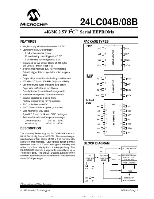
2K位,4K位,8K位和16K位串行I2C总线EEPROM 1. 描述引脚排列CW24C02/02B/02C/04/04A/08/08B/08C/16/16A是电可擦除PROM,分别采用256/512/1024/2048×8-bit的组织结构以及两线串行接口。
电压可允许低至1.8V,待机电流和工作电流分别为1μA和1mA。
CW24C02/02B/02C/04/04A/08/08B/08C/16/16A 具有页写能力,每页分别为8/16/16/16字节。
2. 特点●宽工作电压:1.8V ~ 5.5V●低电压技术- 1mA典型工作电流- 1μA典型待机电流●存储器组织结构- CW24C02,256 X 8(2K bits)- CW24C04,512 X 8(4K bits)- CW24C08,1024 X 8(8K bits)- CW24C16,2048 X 8(16K bits)●2线串行接口,完全兼容I2C总线●I2C时钟频率为1 MHz(5V),400 kHz(1.8V,2.5V,2.7V)●施密特触发输入噪声抑制●硬件数据写保护●内部写周期(最大5 ms)●可按字节写●页写:8字节页(CW24C02),16字节页(CW24C04/08/16)●可按字节,随机和序列读●自动递增地址●ESD保护大于2.5kV(顶视)●高可靠性- 擦写寿命:100万次- 数据保持时间:100年●封装:DIP8L、SOP8L、TSSOP8、DFN8、SOT23-5、TSOT23-5 ●无铅工艺,符合RoHS标准3. 应用领域●智能化仪器仪表●工业控制●家用电器●汽车电子● 计算机/笔记本电脑 ● 通信设备4. 订购信息注:后缀A 或B 是新版本号“A ”版减小了待机电流“B ”版减小了待机电流和写周期 “C ”版同“B ”版5. 框图图1. 框图6. 引脚说明7. 最大额定参数8. 推荐工作条件(应在推荐工作条件下实现功能)9. 引脚电容10. 直流电气特性(推荐工作条件:T11. 交流电气特性图2. 总线时序图3. 写周期时序12. 存储结构13. 详细操作说明13.1 I2C数据总线和传输协议I2C总线接口CW24CXX支持I2C总线传输协议。
HT24LC044K 2-Wire CMOS Serial EEPROMBlock DiagramPin Assignment16th May ¢99Features·Operating voltage:2.4V~5.5V ·Low power consumption -Operation:5mA max.-Standby:5m A max.·Internal organization -4K (HT24LC04):512´8·2-wire serial interface·Write cycle time:5ms max.·Automatic erase-before-write operation·Partial page write allowed ·8-byte page write modes·Write operation with built-in timer ·Hardware controlled write protection ·40-year data retention·106erase/write cycles per word ·8-pin DIP/SOP/TSSOP package ·Commerical temperature range (0°C to +70°C)General DescriptionThe HT24LC04is a 4K-bit serial read/write non-volatile memory device using the CMOS floating gate process.Its 4096bits of memory are organized into 512words and each word is 8bits.The device is optimized for use in many in-dustrial and commercial applications wherelow power and low voltage operation are essen-tial.Up to four HT24LC04devices may be con-nected to the same two-wire bus.The HT24LC04is guaranteed for 1M erase/write cy-cles and 40-year data retention.Pin DescriptionAbsolute Maximum RatingsOperating Temperature (Commercial) ................................................................................. 0°C to 70°C Storage Temperature ....................................................................................................... –50°C to 125°C Applied V CC Voltage with Respect to VSS ........................................................................ –0.3V to 6.0V Applied Voltage on any Pin with Respect to VSS ..................................................................–0.3V to V CC+0.3VNote: These are stress ratings only. Stresses exceeding the range specified under “Absolute Maxi-mum Ratings” may cause substantial damage to the device. Functional operation of this device at other conditions beyond those listed in the specification is not implied and prolonged exposure to extreme conditions may affect device reliability.D.C. Characteristics Ta=0°C to 70°CNote: These parameters are periodically sampled but not 100% tested26th May ’99A.C. Characteristics Ta=0°C to 70°C* The standard mode means V CC=2.4V to 5.5VFor relative timing, refer to timing diagrams36th May ’99Functional Description•Serial clock (SCL)The SCL input is used for positive edge clock data into each EEPROM device and negative edge clock data out of each device.•Serial data (SDA)The SDA pin is bidirectional for serial data transfer. The pin is open-drain driven and may be wired-OR with any number of other open-drain or open collector devices.•A0, A1, A2The HT24LC04 uses the A2 and A1 inputs for hard wire addressing and a total of four 4K devices may be addressed on a single bus system. The A0 pin is not connected. (The device addressing is discussed in detail under the Device Addressing section).•Write protect (WP)The HT24LC04 has a write protect pin that provides hardware data protection. The write protect pin allows normal read/write opera-tions when connected to the V SS. When the write protect pin is connected to Vcc, the write protection feature is enabled and operates asMemory organization•HT24LC04, 4K Serial EEPROMInternally organized with 512 8-bit words, random word addressing requires a 9-bit data word address.Device operations•Clock and data transitionData transfer may be initiated only when the bus is not busy. During data transfer, the data line must remain stable whenever the clockline is high. Changes in data line while the clock line is high will be interpreted as a START or STOP condition.•Start conditionA high-to-low transition of SDA with SCL highis a start condition which must precede any other command (refer to Start and Stop Defi-nition Timing diagram).•Stop conditionA low-to-high transition of SDA with SCL highis a stop condition. After a read sequence, the stop command will place the EEPROM in a standby power mode (refer to Start and Stop Definition Timing Diagram).•AcknowledgeAll addresses and data words are serially transmitted to and from the EEPROM in 8-bit words. The EEPROM sends a zero to acknow-ledge that it has received each word. This happens during the ninth clock cycle.Device addressingThe 4K EEPROM devices require an 8-bit de-vice address word following a start condition to enable the chip for a read or write operation.The device address word consist of a mandatory one, zero sequence for the first four most signifi-cant bits (refer to diagram showing the Device Address). This is common to all the EEPROM device.The next three bits are the A2, A1 and A0 device address bits for the 1K/2K EEPROM. These three bits must compare to their correspondinghard-wired input pins.46th May ’99The 4K EEPROM only use the A2 and A1 device address bits with the third bit as a memory page address bit. The two device address bits must compare to their corresponding hardwired input pins. The A0 pin is not connected.The 8th bit of device address is the read/write operation select bit. A read operation is initi-ated if this bit is high and a write operation is initiated if this bit is low.If the comparison of the device address succeed the EEPROM will output a zero at ACK bit. If not, the chip will return to a standby state.Write operations•Byte writeA write operation requires an 8-bit data word address following the device address word and acknowledgment. Upon receipt of this ad-dress, the EEPROM will again respond with a zero and then clock in the first 8-bit data word. After receiving the 8-bit data word, the EEPROM will output a zero and the address-ing device, such as a microcontroller, must terminate the write sequence with a stop con-dition. At this time the EEPROM enters an internally-timed write cycle to the non-vola-tile memory . All inputs are disabled during this write cycle and EEPROM will not re-spond until the write is completed (refer to Byte write timing).•Page writeThe 4K device is capable of 16-byte page writes.A page write is initiated the same as byte write, but the microcontroller does not send a stop condition after the first data word is clocked in. Instead, after the EEPROM ac-knowledges the receipt of the first data word,the microcontroller can transmit up to fifteen more data words. The EEPROM will respond with a zero after each data word received. The microcontroller must terminate the page write sequence with a stop condition.The data word address lower four bits are internally incremented following the receipt of each data word. The higher data word ad-dress bits are not incremented, retaining the memory page row location (refer to Page write timing).•Acknowledge pollingSince the device will not acknowledge during a write cycle, this can be used to determine when the cycle is complete (this feature can be used to maximize bus throughput). Once the stop condition for a write command has been issued from the master, the device initiates the internally timed write cycle. ACK polling can be initiated immediately . This involves the master sending a start condition followed by the control byte for a write command (R/W=0). If the device is still busy with the write cycle, then no ACK will be returned. If the cycle is completed, then the device will return the ACK and the master can then pro-ceed with the next read or write command.•Write protectThe HT24LC04 can be used as a serial ROM when the WP pin is connected to VCC. Pro-gramming will be inhibited and the entire memory will be write-protected.•Read operationsRead operations are initiated the same way as write operations with the exception that the read/write select bit in the device address word is set to one. There are three read opera-tions: current address read, random address read and sequential read.•Current address readThe internal data word address counter main-tains the last address accessed during the last read or write operation, incremented by one.This address stays valid between operations as long as the chip power is maintained. The address roll over during read from the last byte of the last memory page to the first byte of the first page. The address roll over during write from the last byte of the current page to the first byte of the same page. Once the de-vice address with the read/write select bit set to one is clocked in and acknowledged by the EEPROM, the current address data word is serially clocked out. The microcontroller does not respond with an input zero but generates a following stop condition (refer to Current read timing).•Random readA random read requires a dummy byte write sequence to load in the data word address which is then clocked in and acknowledged by the EEPROM. The microcontroller must then generate another start condition. The micro-controller now initiates a current address read by sending a device address with the read/write select bit high. The EEPROM ac-knowledges the device address and serially clocks out the data word. The microcontroller does not respond with a zero but does gener-ates a following stop condition (refer to Ran-dom read timing).Acknowledge polling flowHT24LC0466th May ’99Timing DiagramsNote: The write cycle time t WR is the time from a valid stop condition of a write sequence to the end of the valid start condition of sequential command.•Sequential readSequential reads are initiated by either a cur-rent address read or a random address read.After the microcontroller receives a data word,it responds with an acknowledgment. As long as the EEPROM receives an acknowledgment, it will continue to increment the data word ad-dress and serially clock out sequential datawords. When the memory address limit is reached, the data word address will roll over and the sequential read continues. The se-quential read operation is terminated when the microcontroller does not respond with a zero but generates a following stop condition(refer to Sequential read timing).Holtek Semiconductor Inc. (Headquarters)No.3 Creation Rd. II, Science-based Industrial Park, Hsinchu, Taiwan, R.O.C.Tel: 886-3-563-1999Fax: 886-3-563-1189Holtek Semiconductor Inc. (Taipei Office)5F, No.576, Sec.7 Chung Hsiao E. Rd., Taipei, Taiwan, R.O.C.Tel: 886-2-2782-9635Fax: 886-2-2782-9636Fax: 886-2-2782-7128 (International sales hotline)Holtek Microelectronics Enterprises Ltd.RM.711, Tower 2, Cheung Sha Wan Plaza, 833 Cheung Sha Wan Rd., Kowloon, Hong KongTel: 852-2-745-8288Fax: 852-2-742-865786th May ’99。
日期:CATALOGUE目录•晶体管基础•晶体管的应用电路•晶体管的选型与检测•晶体管的实际应用与未来发展晶体管基础定义工作原理晶体管定义与原理晶体管由三个区域组成,分别是基区、发射区和集电区,各区域之间通过结隔离,形成三个电极,即基极、发射极和集电极。
晶体管类型与结构结构NPN型与PNP型电流放大系数饱和压降击穿电压最大耗散功率晶体管主要参数晶体管的应用电路常见类型共射放大电路、共基放大电路、共集放大电路等。
工作原理晶体管放大电路利用晶体管的放大效应,将输入信号放大后输出。
通过选择合适的电路参数,可以实现电压放大、电流放大或功率放大。
应用领域音频放大、射频放大、信号驱动等。
工作原理01常见类型02应用领域03常见类型应用领域晶体管的选型与检测工作电压和电流频率特性增益和功率封装和散热01020304晶体管的选型原则外观检查万用表检测功能性测试030201晶体管检测方法与步骤晶体管常见故障排除开路故障短路故障参数异常热稳定性问题晶体管的实际应用与未来发展放大器电路通过晶体管的导通与截止特性,可实现基本的逻辑门功能,如AND、OR、NOT门等,进而构建复杂的数字电路。
数字逻辑门电源管理晶体管在电子领域的应用实例体积小巧功耗低速度快晶体管与其他元器件的比较优势未来发展趋势与新技术应用展望碳化硅晶体管柔性晶体管集成电路中的晶体管微缩感谢观看。