TI(德州仪器)公司产品导购手册
- 格式:pdf
- 大小:1.23 MB
- 文档页数:56

IMPORTANT NOTICETexas Instruments Incorporated and its subsidiaries (TI) reserve the right to make corrections, modifications, enhancements, improvements, and other changes to its products and services at any time and to discontinue any product or service without notice. Customers should obtain the latest relevant information before placing orders and should verify that such information is current and complete. All products are sold subject to TI’s terms and conditions of sale supplied at the time of order acknowledgment.TI warrants performance of its hardware products to the specifications applicable at the time of sale in accordance with TI’s standard warranty. T esting and other quality control techniques are used to the extent TI deems necessary to support this warranty. Except where mandated by government requirements, testing of all parameters of each product is not necessarily performed.TI assumes no liability for applications assistance or customer product design. Customers are responsible for their products and applications using TI components. T o minimize the risks associated with customer products and applications, customers should provide adequate design and operating safeguards.TI does not warrant or represent that any license, either express or implied, is granted under any TI patent right, copyright, mask work right, or other TI intellectual property right relating to any combination, machine, or process in which TI products or services are used. Information published by TI regarding third−party products or services does not constitute a license from TI to use such products or services or a warranty or endorsement thereof. Use of such information may require a license from a third party under the patents or other intellectual property of the third party, or a license from TI under the patents or other intellectual property of TI.Reproduction of information in TI data books or data sheets is permissible only if reproduction is without alteration and is accompanied by all associated warranties, conditions, limitations, and notices. Reproduction of this information with alteration is an unfair and deceptive business practice. TI is not responsible or liable for such altered documentation.Resale of TI products or services with statements different from or beyond the parameters stated by TI for that product or service voids all express and any implied warranties for the associated TI product or service and is an unfair and deceptive business practice. TI is not responsible or liable for any such statements.Mailing Address:Texas InstrumentsPost Office Box 655303Dallas, Texas 75265Copyright 2001, Texas Instruments IncorporatedEVM IMPORTANT NOTICETexas Instruments (TI) provides the enclosed product(s) under the following conditions:This evaluation kit being sold by TI is intended for use for ENGINEERING DEVELOPMENT OR EVALUATION PURPOSES ONLY and is not considered by TI to be fit for commercial use. As such, the goods being provided may not be complete in terms of required design-, marketing-, and/or manufacturing-related protective considerations, including product safety measures typically found in the end product incorporating the goods. As a prototype, this product does not fall within the scope of the European Union directive on electromagnetic compatibility and therefore may not meet the technical requirements of the directive.Should this evaluation kit not meet the specifications indicated in the EVM User’s Guide, the kit may be returned within 30 days from the date of delivery for a full refund. THE FOREGOING WARRANTY IS THE EXCLUSIVE WARRANTY MADE BY SELLER TO BUYER AND IS IN LIEU OF ALL OTHER WARRANTIES, EXPRESSED, IMPLIED, OR STATUTORY, INCLUDING ANY WARRANTY OF MERCHANTABILITY OR FITNESS FOR ANY PARTICULAR PURPOSE.The user assumes all responsibility and liability for proper and safe handling of the goods. Further, the user indemnifies TI from all claims arising from the handling or use of the goods. Please be aware that the products received may not be regulatory compliant or agency certified (FCC, UL, CE, etc.). Due to the open construction of the product, it is the user’s responsibility to take any and all appropriate precautions with regard to electrostatic discharge.EXCEPT TO THE EXTENT OF THE INDEMNITY SET FORTH ABOVE, NEITHER PARTY SHALL BE LIABLE TO THE OTHER FOR ANY INDIRECT, SPECIAL, INCIDENTAL, OR CONSEQUENTIAL DAMAGES.TI currently deals with a variety of customers for products, and therefore our arrangement with the user is not exclusive.TI assumes no liability for applications assistance, customer product design, software performance, or infringement of patents or services described herein.Please read the EVM User’s Guide and, specifically, the EVM Warnings and Restrictions notice in the EVM User’s Guide prior to handling the product. This notice contains important safety information about temperatures and voltages. For further safety concerns, please contact the TI application engineer.Persons handling the product must have electronics training and observe good laboratory practice standards. No license is granted under any patent right or other intellectual property right of TI covering or relating to any machine, process, or combination in which such TI products or services might be or are used.Mailing Address:Texas InstrumentsPost Office Box 655303Dallas, Texas 75265Copyright 2001, Texas Instruments IncorporatedEVM WARNINGS AND RESTRICTIONSIt is important to operate this EVM within the input voltage range of 85 V to 265 V and the output voltage of 12 V +/− 5%.Exceeding the specified input range may cause unexpected operation and/or irreversible damage to the EVM. If there are questions concerning the input range, please contact a TI field representative prior to connecting the input power.Applying loads outside of the specified output range may result in unintended operation and/or possible permanent damage to the EVM. Please consult the EVM User’s Guide prior to connecting any load to the EVM output. If there is uncertainty as to the load specification, please contact a TI field representative.During normal operation, some circuit components may have case temperatures greater than 50°C. The EVM is designed to operate properly with certain components above 50°C as long as the input and output ranges are maintained. These components include but are not limited to linear regulators, switching transistors, pass transistors, and current sense resistors. These types of devices can be identified using the EVM schematic located in the EVM User’s Guide. When placing measurement probes near these devices during operation, please be aware that these devices may be very warm to the touch.Mailing Address:Texas InstrumentsPost Office Box 655303Dallas, Texas 75265Copyright 2001, Texas Instruments IncorporatedContentsContents. . . . . . . . . . . . . . . . . . . . . . . . . . . . . . . . . . . . . . . . . . . . . . . . . . . . . . . . . . . . .1General Information1-1 . . . . . . . . . . . . . . . . . . . . . . . . . . . . . . . . . . . . . . . . . . . . . . . . . . . . . . . . . . . . . . . . . .1.1Features1-2. . . . . . . . . . . . . . . . . . . . . . . . . . . . . . . . . . . . . . . . . . . . . . . . . . . . . . . . . . . . . . . .1.2Description1-2. . . . . . . . . . . . . . . . . . . . . . . . . . . . . . . . . . . . . . . . . . . . . . . . . . . . . . . .1.3Operating Guidelines1-3. . . . . . . . . . . . . . . . . . . . . . . . . . . . . . . . . . . . . . . . . . . .1.3.1Step 1. Load Connections1-3. . . . . . . . . . . . . . . . . . . . . . . . . . . . . . . . . . . . . . . . .1.3.2Step2. Applying Input Power1-3. . . . . . . . . . . . .1.3.3Step 3. Evaluating the Demonstration’s Boards Performance.1-3. . . . . . . . . . . . . . . . . . . . . . . . . . . . . . . . . . . . . . . . . . . . . . . .1.3.4Additional Information1-3. . . . . . . . . . . . . . . . . . . . . . . . . . . . . . . . . . . . . . . . . . . . . . . . .1.4DM38500 EVM Performance1-5. . . . . . . . . . . . . . . . . . . . . . . . . . . . . . . . . . . . . . . . . . . . . . . . . . . . . . . . . . . . . . . . . . . . . . .2Reference2-1. . . . . . . . . . . . . . . . . . . . . . . . . . . . . . . . . . . . . . . . . . . . .2.1DM38500 EVM Part Descriptions2-2. . . . . . . . . . . . . . . . . . . . . . . . . . . . . . . . . . . . . . . . . . . . . . . . . . . .2.2DM38500 Board Layouts2-4Figures. . . . . . . . . . . . . . . . . . . . . . . . . . . .1−1.DM38500 Evaluation Module Application Schematic1-4. . . . . . . . . . . . . . . . . . . . . . . . . . . . . . . . . . . . . .1−2.DM38500 EVM Response, VCC = +15 V1-5. . . . . . . . . . . . . . . . . . . . . . . . . . . . . . . . . . . . . . . . . . .1−3.DM38500 Response, VCC = +15 V1-5. . . . . . . . . . . . . . . . . . . . . . . . . . . . . . . . . . . . . . . . . . .1−4.DM38500 Response, VCC = +15 V1-6. . . . . . . . . . . . . . . . . . . . . . . . . . . . . . . . . . . . . .2−1.DM38500 EVM PC Board: Top Assembly2-4Chapter 1GeneralInformationThis chapter details the Texas Instruments (TI) DM38500 PFC/PWM Combination Controller 100W Power Factor Correction Preregulator Evaluation Module (EVM) SLUU068. It includes a list of EVM features, a brief description of the module illustrated with a pictorial, schematic diagrams, and EVM specifications.Topic Page . . . . . . . . . . . . . . . . . . . . . . . . . . . . . . . . . . . . . . . . . . . . . . . . . . . . .1.1Features1−2. . . . . . . . . . . . . . . . . . . . . . . . . . . . . . . . . . . . . . . . . . . . . . . . . . .1.2Description1−2 1.3Operating Guidelines1−3. . . . . . . . . . . . . . . . . . . . . . . . . . . . . . . . . . . . . . . . . .1.4DM38500 EVM Performance1−5. . . . . . . . . . . . . . . . . . . . . . . . . . . . . . . . . . . .General Information1-1Features1.1FeaturesUCC38500 PFC/PWM Combination Controller 100W Power Factor Correc-tion Preregulator include:J Combines PFC and 2nd Stage Down Converter ControlsJ Controls Boost Preregulator to Near-unity Power FactorJ Accurate Power LimitingJ Improved Feedforward Line RegulationJ Peak Current Mode Control in Second StageJ Programmable OscillatorJ Leading Edge/Trailing Edge Modulation for Reduced Output RippleJ Low Startup Supply CurrentJ Synchronized Second Stage with Programmable Soft-startJ Programmable Second Stage Shut-down1.2DescriptionThe UCC38500 provides all the functions necessary for active power factorcorrection and a second stage dc-to-dc converter all in one integrated circuit.The control IC uses leading edge modulation for the boost stage and trailingedge modulation for the step down converter to reduce the RMS current in theboost capacitor. The dc-to-dc controller uses peak current mode control foreasy loop compensation.The UCC38500 evaluation board is designed to illustrate the performance ofthe IC in a complete off-line 100W two-stage power converter using power fac-tor correction. The demonstration board was designed to operate with a uni-versal input voltage range (i.e. 85−265 Vac) with a regulated 12V dc output.CautionHigh-voltage levels are present on the evaluation module whenever it isenergized. Proper precautions must be taken when working with theEVM. The output capacitor has high levels of energy storage and it mustbe discharged before the load is removed. Serious injury can occur ifproper safety precautions are not followed.1-2Description1-3General Information 1.3Operating GuidelinesThe operating guidelines for the evaluation board are provided with reference to the schematic in Figure 1−1 and the component layout in Figure 2−1.1.3.1Step 1. Load ConnectionsA resistive or electronic load can be applied to the output terminals labeled OUT− and OUT+.Note: For safety reasons the load should be connected before power is sup-plied to the demonstration board.1.3.2Step2. Applying Input PowerA 60 Hz AC power source not exceeding 265 V RMS needs be applied across terminals AC−N and AC−L for proper operation.1.3.3Step 3. Evaluating the Demonstration’s Boards Performance.With the AC source set between 85−265 V RMS the output voltage should be regulated and the input current should track the input voltage shape with near unity power factor. The operation of the circuit is verified over the line and load range and shows efficiency as high as 85%. At lighter loads, there may be some distortion in the line current due to Discontinuous Conduction Mode (DCM) operation. Please refer to Figures 1−2, 1−3 and 1−4 for typical EVM performance.1.3.4Additional InformationFor more information, pin description and specifications for the UCC38500PFC/PWM Combination Controller, please refer to the datasheet or contact the Texas Instruments Semiconductor Product Information Center at 1-800-336-5236 or 1-972-644-5580. Product Information can also be found on the World Wide Web at .Description1-4Figure 1−1.DM38500 Evaluation Module Application SchematicUDG−000941210952611137843116171518191420O V P /E N B L V S E N S E V A O U T I S E N S E M O U TC A O U T I A C V F FP K L I M I T V R E F G T 1G T 2V C C C T R T G N D P W R G N D S S 2V E R R I S E N S E 2U C C 38500V R E FQ 5R 25V C CR 7R 6G T 1G T 2D 10D 9C 27P K L I M I TC 28R 17C 19C 22R 28C 25R 23R 34R 21R 22R 33R 20C 2R 15R 5L 1D 3D 1G T 1R 14R 29P K L I M I TR 19C 26V R E F R 18R 24C 29C 30I S E N S E 2G T 2R 13R 2C 5P W R G N D G T 212 V 100 W +−L 2T 1Q 2Q 1Q 3D 11V A C 85−265V R M SD 6D 4T 2D 8U 4C 7S G N DS G N D S G N DP G N D 2P G N DP G N DP G N DP G N DS G N D P G N D D 5D 7C 12C 20L 1V C C B I A S C I R C U I TV C CV C C B I A S C I R C U I TP G N D C 23P G N D 2P G N D 2R 26D 14R 36R 16C 14R 35R 32R 27D 13R 31C 8R 30R 10R 12R 11C 21C 16C 3P G N D C 24D 2R 1C 4C 18R 4D 15D 12D 16A C −NA C −LO U T +O U T −V R E FR 3R 39C 13I S E N S E 2C 17H 11A V 1321456U 3S G N D C 6C 38H I G H V O L T A G E −S E E E V M W A R N I N G S A N D R E S T R I C T I O N SH I G H T E M P E R A T U R E −S E E E V M W A R N I N G S A N D R E S T R I C T I O N SH I G H V O L T A G E −S E E E V M W A R N I N G S A N D R E S T R I C T I O N S H I G H T E M P E R A T U R E −S E E E V M W A R N I N G S A N D R E S T R I C T I O N S Note: High-Voltage component. See EVM Warnings and Restrictions at the back of this document. Note: High-T emperature component. See EVM Warnings and Restrictions at the back of this document.DM38500 EVM Performance1-5General Information 1.4DM38500 EVM PerformanceFigure 1−2 through 1−4 shows the typical evaluation module performance.Figure 1−2.DM38500 EVM EfficiencyUCC38500 EFFICIENCYvsOUTPUT POWER 505560657075808590201040306050807090100V IN = 85 VV IN = 175 VV IN = 265 VP OUT − WE f f i c i e n c y −%Figure 1−3.DM38500 Power FactorUCC38500 PFvsOUTPUT POWERP OUT − WP o w e r F a c t o r0.852010403060508070901000.900.951.00V IN = 85 V V IN = 175 VV IN = 265 VDM38500 EVM Performance1-6Figure 1−4.DM38500 Total Harmonic Distortion5101520253020104030605080709010035UCC38500 TOTAL HARMONIC DISTORTIONvsOUTPUT POWERP OUT − WT o t a l H a r m o n i c D i s t o r t i o nV IN = 85 VV IN = 175 VV IN = 265 V2-1ReferenceReferenceThis chapter includes a parts list and PCB layout illustrations for the DM38500EVM.TopicPage2.1DM38500 EVM Part Descriptions 2−2. . . . . . . . . . . . . . . . . . . . . . . . . . . 2.2DM38500 Board Layouts 2−4. . . . . . . . . . . . . . . . . . . . . . . . . . . . . . . . . . Chapter 2DM38500 EVM Part Descriptions2-22.1DM38500 EVM Part DescriptionsTable 2−1.DM38500 Part DescriptionsDescriptionReference Qty Value/Type Number Manufacturer Part Number C12, C20,C293 1 µF, 50 V, polypropylene Panasonic ECQ−V1H105JL C13147 pF, 50 V, ceramic Panasonic ECU−S2A470JCA C7, C16,C14310 nF, 50 V, ceramic Panasonic ECU−S1H103JCB C17, C382100 pF, 50 V, ceramic Panasonic ECU−S1H101JCA C191 2.2 nF, 50 V, ceramic Panasonic ECU−S1H222JCB C21470 nF, 400 V, polypropylenePanasonic ECQ−E4474KZ C211680 pF, 50 V, ceramic Panasonic ECU−S1H681JCB CapacitorsC221390 pF, 50 V, ceramic Panasonic ECU−S1H391JCA C241100 pF, 50 V, ceramic Panasonic ECU−S1H101JCA C251150 nF, 50 V, ceramicPanasonic ECU−S1H154KBB C26147 nF, 600 V, polypropylene Panasonic ECQ−E6473KF C27, C182100 pF, 50 V, ceramic Panasonic ECU−S1H105KBB C28, C232 2.2 µF, 50 V, ceramicPanasonic ECU−S1H225MEB C31100 µF, 450 V, electrolytic Panasonic ECO−S2WB101BA C3011800 µF, 25 V, electrolytic Panasonic ECA−IEFQ182C4, C5, C830.1 µF, 50 V, ceramic Panasonic ECU−S1H104KBB C61100 µF, 25 V, electrolytic Panasonic EEU−FCIE101S D11 6 A, 600 V, GI756CTGeneral Inst.GI756CT D111 6 A, 600 V, bridge rectifier,PB66Diodes Inc.PB66D121 1 A, 40 V, Shottky SR103CT D131TL431CLPTITL431C D14110 V, 1 W, Zener 1N4740D15, D2218 V, 1 W, Zener 1N4746DiodesD31 6 A, 600 V, ultra fast IR HFA08TB60−ND D4, D62 1 A, 600 V, fast recovery PhilipsBYV26C D5,D7,D9,D10, D165 1 A, 40 V, Shottky 1N5819D81 6 A, 600 V, full wave rectifierIRHBR2045FH1, FH223AG Fuse clip Fuses F11 6 A, 250 V HS31For Q3Aavid 513201HS4, HS52For D3 and D8Aavid 579302 B 0 00 00Heat sinks HS1, HS22For Q1 and Q2Avid 593002 B 0 34 00L11 1.7 mH, 2.5 A, coupled Cooper CTX08−14730Inductors L2135 µH, 8.3 ACooper CTX08−14279Q1,Q228 A, 500 V, n−channel IR IRF840Q3114 A, 500 V, n−channel IRIRFP450MOSFETsQ51NPN transistor MJE13005Not usedQ4, R8, R9,C9, C15,C106Not usedDM38500 EVM Part Descriptions2-3Reference DescriptionReference Qty Value/Type Number ManufacturerPart Number R1, R122ShortR10, R362200 Ω, ¼ W R25, R29,R27310 k Ω, ¼ WR131 2 k Ω, ¼ W R141 1.5 k Ω, ¼ W R15, R192 3.92 k Ω, ¼ W R161750 Ω, ¼ W R1717.5 k Ω, ¼ W R18, R242392 k Ω, ¼ W R2, R112 1 k Ω, ¼ W R20122.1 k Ω, ¼ W R2118.25 k Ω, ¼ W R22, R332562 k Ω, ¼ W ResistorsR231200 k Ω, ¼ W R261100 Ω, ¼ WR281100 k Ω, ¼ W R30130.1 k Ω, ¼ W R31133.2 k Ω, ¼ W R321 4.75 k Ω, ¼ W R341221 k Ω, ¼ W R35116.2 k Ω, ¼ W R391 1 k Ω, 1 W R41 1 Ω, 1 W, ±5%R510.33 Ω, 3 W, ±5%R6, R7220 Ω, ¼ WR3151 k Ω, 2 W, 400 VT118 mH, 10 A, 10.8:1Cooper CTX08−14226Transformers T21560−990 µH, 1:1 gate drive Cooper CTX08−14225U41BiCMOS PFC/PWM combination controller TexasInstrumentsUCC38500N ICsU31Opto-isolator4N36X13Thermal pad TO−220(@ Q1, Q2, D8)X21Thermal pad TO−247(@ Q3)MiscellaneousX34Screw pan head #4−40 X 7/16 (@Q1, Q2, Q3, D8)X44Nut #4x40X53Nylon shoulder washer #4(@Q1, Q2, D8)X61Bevel washer #4 (@Q3)PCBPCB1Bare boardUCC38500 PCBNotes:1)The values of these components are to be determined by the user in accordance with the applica-tion requirements.2)Unless otherwise specified, all resistors have a tolerance of ±1%.3)Capacitor C38 is located at reference designator R38 on the PCB.。
TEXAS INSTRUMENTS-PRODUCTION DATAStellaris®LM3S2793MicrocontrollerDATA SHEETCopyright©2007-2012 DS-LM3S2793-11425CopyrightCopyright©2007-2012Texas Instruments Incorporated All rights reserved.Stellaris and StellarisWare®are registered trademarks of Texas Instruments Incorporated.ARM and Thumb are registered trademarks and Cortex is a trademark of ARM Limited.Other names and brands may be claimed as the property of others.PRODUCTION DATA information is current as of publication date.Products conform to specifications per the terms of Texas Instruments standard warranty.Production processing does not necessarily include testing of all parameters.Please be aware that an important notice concerning availability,standard warranty,and use in critical applications of Texas Instruments semiconductor products and disclaimers thereto appears at the end of this data sheet.Texas Instruments Incorporated108Wild Basin,Suite350Austin,TX78746/stellaris/sc/technical-support/product-information-centers.htmStellaris®LM3S2793MicrocontrollerTable of ContentsRevision History (32)About This Document (43)Audience (43)About This Manual (43)Related Documents (43)Documentation Conventions (44)1Architectural Overview (46)1.1Overview (46)1.2Target Applications (48)1.3Features (48)1.3.1ARM Cortex-M3Processor Core (48)1.3.2On-Chip Memory (50)1.3.3External Peripheral Interface (51)1.3.4Serial Communications Peripherals (53)1.3.5System Integration (57)1.3.6Advanced Motion Control (63)1.3.7Analog (65)1.3.8JTAG and ARM Serial Wire Debug (66)1.3.9Packaging and Temperature (67)1.4Hardware Details (67)2The Cortex-M3Processor (68)2.1Block Diagram (69)2.2Overview (70)2.2.1System-Level Interface (70)2.2.2Integrated Configurable Debug (70)2.2.3Trace Port Interface Unit(TPIU) (71)2.2.4Cortex-M3System Component Details (71)2.3Programming Model (72)2.3.1Processor Mode and Privilege Levels for Software Execution (72)2.3.2Stacks (72)2.3.3Register Map (73)2.3.4Register Descriptions (74)2.3.5Exceptions and Interrupts (87)2.3.6Data Types (87)2.4Memory Model (87)2.4.1Memory Regions,Types and Attributes (89)2.4.2Memory System Ordering of Memory Accesses (90)2.4.3Behavior of Memory Accesses (90)2.4.4Software Ordering of Memory Accesses (91)2.4.5Bit-Banding (92)2.4.6Data Storage (94)2.4.7Synchronization Primitives (95)2.5Exception Model (96)2.5.1Exception States (97)2.5.2Exception Types (97)Table of Contents2.5.3Exception Handlers (100)2.5.4Vector Table (100)2.5.5Exception Priorities (101)2.5.6Interrupt Priority Grouping (102)2.5.7Exception Entry and Return (102)2.6Fault Handling (104)2.6.1Fault Types (104)2.6.2Fault Escalation and Hard Faults (105)2.6.3Fault Status Registers and Fault Address Registers (106)2.6.4Lockup (106)2.7Power Management (106)2.7.1Entering Sleep Modes (106)2.7.2Wake Up from Sleep Mode (107)2.8Instruction Set Summary (108)3Cortex-M3Peripherals (111)3.1Functional Description (111)3.1.1System Timer(SysTick) (111)3.1.2Nested Vectored Interrupt Controller(NVIC) (112)3.1.3System Control Block(SCB) (114)3.1.4Memory Protection Unit(MPU) (114)3.2Register Map (119)3.3System Timer(SysTick)Register Descriptions (121)3.4NVIC Register Descriptions (125)3.5System Control Block(SCB)Register Descriptions (138)3.6Memory Protection Unit(MPU)Register Descriptions (167)4JTAG Interface (177)4.1Block Diagram (178)4.2Signal Description (178)4.3Functional Description (179)4.3.1JTAG Interface Pins (179)4.3.2JTAG TAP Controller (181)4.3.3Shift Registers (181)4.3.4Operational Considerations (182)4.4Initialization and Configuration (184)4.5Register Descriptions (185)4.5.1Instruction Register(IR) (185)4.5.2Data Registers (187)5System Control (189)5.1Signal Description (189)5.2Functional Description (189)5.2.1Device Identification (190)5.2.2Reset Control (190)5.2.3Non-Maskable Interrupt (195)5.2.4Power Control (195)5.2.5Clock Control (196)5.2.6System Control (203)5.3Initialization and Configuration (205)5.4Register Map (205)Stellaris®LM3S2793Microcontroller5.5Register Descriptions (207)6Hibernation Module (295)6.1Block Diagram (296)6.2Signal Description (296)6.3Functional Description (297)6.3.1Register Access Timing (297)6.3.2Hibernation Clock Source (298)6.3.3System Implementation (299)6.3.4Battery Management (300)6.3.5Real-Time Clock (300)6.3.6Battery-Backed Memory (301)6.3.7Power Control Using HIB (301)6.3.8Power Control Using VDD3ON Mode (301)6.3.9Initiating Hibernate (301)6.3.10Waking from Hibernate (301)6.3.11Interrupts and Status (302)6.4Initialization and Configuration (302)6.4.1Initialization (302)6.4.2RTC Match Functionality(No Hibernation) (303)6.4.3RTC Match/Wake-Up from Hibernation (303)6.4.4External Wake-Up from Hibernation (304)6.4.5RTC or External Wake-Up from Hibernation (304)6.5Register Map (304)6.6Register Descriptions (305)7Internal Memory (322)7.1Block Diagram (322)7.2Functional Description (322)7.2.1SRAM (323)7.2.2ROM (323)7.2.3Flash Memory (325)7.3Register Map (330)7.4Flash Memory Register Descriptions(Flash Control Offset) (331)7.5Memory Register Descriptions(System Control Offset) (343)8Micro Direct Memory Access(μDMA) (359)8.1Block Diagram (360)8.2Functional Description (360)8.2.1Channel Assignments (361)8.2.2Priority (362)8.2.3Arbitration Size (362)8.2.4Request Types (362)8.2.5Channel Configuration (363)8.2.6Transfer Modes (365)8.2.7Transfer Size and Increment (373)8.2.8Peripheral Interface (373)8.2.9Software Request (373)8.2.10Interrupts and Errors (374)8.3Initialization and Configuration (374)8.3.1Module Initialization (374)Table of Contents8.3.2Configuring a Memory-to-Memory Transfer (374)8.3.3Configuring a Peripheral for Simple Transmit (376)8.3.4Configuring a Peripheral for Ping-Pong Receive (377)8.3.5Configuring Channel Assignments (380)8.4Register Map (380)8.5μDMA Channel Control Structure (381)8.6μDMA Register Descriptions (388)9General-Purpose Input/Outputs(GPIOs) (417)9.1Signal Description (417)9.2Functional Description (422)9.2.1Data Control (423)9.2.2Interrupt Control (424)9.2.3Mode Control (425)9.2.4Commit Control (425)9.2.5Pad Control (426)9.2.6Identification (426)9.3Initialization and Configuration (426)9.4Register Map (427)9.5Register Descriptions (430)10External Peripheral Interface(EPI) (473)10.1EPI Block Diagram (474)10.2Signal Description (475)10.3Functional Description (477)10.3.1Non-Blocking Reads (478)10.3.2DMA Operation (479)10.4Initialization and Configuration (479)10.4.1SDRAM Mode (480)10.4.2Host Bus Mode (484)10.4.3General-Purpose Mode (495)10.5Register Map (503)10.6Register Descriptions (504)11General-Purpose Timers (546)11.1Block Diagram (547)11.2Signal Description (547)11.3Functional Description (550)11.3.1GPTM Reset Conditions (551)11.3.2Timer Modes (551)11.3.3DMA Operation (557)11.3.4Accessing Concatenated Register Values (558)11.4Initialization and Configuration (558)11.4.1One-Shot/Periodic Timer Mode (558)11.4.2Real-Time Clock(RTC)Mode (559)11.4.3Input Edge-Count Mode (559)11.4.4Input Edge Timing Mode (560)11.4.5PWM Mode (561)11.5Register Map (561)11.6Register Descriptions (562)Stellaris®LM3S2793Microcontroller 12Watchdog Timers (593)12.1Block Diagram (594)12.2Functional Description (594)12.2.1Register Access Timing (595)12.3Initialization and Configuration (595)12.4Register Map (595)12.5Register Descriptions (596)13Analog-to-Digital Converter(ADC) (618)13.1Block Diagram (619)13.2Signal Description (620)13.3Functional Description (622)13.3.1Sample Sequencers (622)13.3.2Module Control (623)13.3.3Hardware Sample Averaging Circuit (625)13.3.4Analog-to-Digital Converter (626)13.3.5Differential Sampling (629)13.3.6Internal Temperature Sensor (632)13.3.7Digital Comparator Unit (632)13.4Initialization and Configuration (637)13.4.1Module Initialization (637)13.4.2Sample Sequencer Configuration (638)13.5Register Map (638)13.6Register Descriptions (640)14Universal Asynchronous Receivers/Transmitters(UARTs) (698)14.1Block Diagram (699)14.2Signal Description (699)14.3Functional Description (701)14.3.1Transmit/Receive Logic (701)14.3.2Baud-Rate Generation (702)14.3.3Data Transmission (703)14.3.4Serial IR(SIR) (703)14.3.5ISO7816Support (704)14.3.6Modem Handshake Support (704)14.3.7LIN Support (706)14.3.8FIFO Operation (707)14.3.9Interrupts (708)14.3.10Loopback Operation (709)14.3.11DMA Operation (709)14.4Initialization and Configuration (709)14.5Register Map (710)14.6Register Descriptions (712)15Synchronous Serial Interface(SSI) (762)15.1Block Diagram (763)15.2Signal Description (763)15.3Functional Description (764)15.3.1Bit Rate Generation (765)15.3.2FIFO Operation (765)15.3.3Interrupts (765)Table of Contents15.3.4Frame Formats (766)15.3.5DMA Operation (773)15.4Initialization and Configuration (774)15.5Register Map (775)15.6Register Descriptions (776)16Inter-Integrated Circuit(I2C)Interface (804)16.1Block Diagram (805)16.2Signal Description (805)16.3Functional Description (806)16.3.1I2C Bus Functional Overview (806)16.3.2Available Speed Modes (808)16.3.3Interrupts (809)16.3.4Loopback Operation (810)16.3.5Command Sequence Flow Charts (811)16.4Initialization and Configuration (818)16.5Register Map (819)16.6Register Descriptions(I2C Master) (820)16.7Register Descriptions(I2C Slave) (833)17Inter-Integrated Circuit Sound(I2S)Interface (842)17.1Block Diagram (843)17.2Signal Description (843)17.3Functional Description (845)17.3.1Transmit (846)17.3.2Receive (850)17.4Initialization and Configuration (852)17.5Register Map (853)17.6Register Descriptions (854)18Controller Area Network(CAN)Module (879)18.1Block Diagram (880)18.2Signal Description (880)18.3Functional Description (881)18.3.1Initialization (882)18.3.2Operation (883)18.3.3Transmitting Message Objects (884)18.3.4Configuring a Transmit Message Object (884)18.3.5Updating a Transmit Message Object (885)18.3.6Accepting Received Message Objects (886)18.3.7Receiving a Data Frame (886)18.3.8Receiving a Remote Frame (886)18.3.9Receive/Transmit Priority (887)18.3.10Configuring a Receive Message Object (887)18.3.11Handling of Received Message Objects (888)18.3.12Handling of Interrupts (890)18.3.13Test Mode (891)18.3.14Bit Timing Configuration Error Considerations (893)18.3.15Bit Time and Bit Rate (893)18.3.16Calculating the Bit Timing Parameters (895)Stellaris®LM3S2793Microcontroller 18.4Register Map (898)18.5CAN Register Descriptions (899)19Analog Comparators (930)19.1Block Diagram (931)19.2Signal Description (931)19.3Functional Description (932)19.3.1Internal Reference Programming (933)19.4Initialization and Configuration (934)19.5Register Map (935)19.6Register Descriptions (936)20Pulse Width Modulator(PWM) (944)20.1Block Diagram (945)20.2Signal Description (946)20.3Functional Description (949)20.3.1PWM Timer (949)20.3.2PWM Comparators (950)20.3.3PWM Signal Generator (951)20.3.4Dead-Band Generator (952)20.3.5Interrupt/ADC-Trigger Selector (952)20.3.6Synchronization Methods (953)20.3.7Fault Conditions (954)20.3.8Output Control Block (954)20.4Initialization and Configuration (955)20.5Register Map (956)20.6Register Descriptions (959)21Quadrature Encoder Interface(QEI) (1022)21.1Block Diagram (1022)21.2Signal Description (1023)21.3Functional Description (1024)21.4Initialization and Configuration (1027)21.5Register Map (1027)21.6Register Descriptions (1028)22Pin Diagram (1045)23Signal Tables (1047)23.1100-Pin LQFP Package Pin Tables (1048)23.2108-Ball BGA Package Pin Tables (1084)23.3Connections for Unused Signals (1120)24Operating Characteristics (1122)25Electrical Characteristics (1123)25.1Maximum Ratings (1123)25.2Recommended Operating Conditions (1123)25.3Load Conditions (1124)25.4JTAG and Boundary Scan (1124)25.5Power and Brown-Out (1126)25.6Reset (1127)25.7On-Chip Low Drop-Out(LDO)Regulator (1128)25.8Clocks (1128)Table of Contents25.8.1PLL Specifications (1128)25.8.2PIOSC Specifications (1129)25.8.3Internal30-kHz Oscillator Specifications (1129)25.8.4Hibernation Clock Source Specifications (1130)25.8.5Main Oscillator Specifications (1130)25.8.6System Clock Specification with ADC Operation (1131)25.9Sleep Modes (1131)25.10Hibernation Module (1131)25.11Flash Memory (1133)25.12Input/Output Characteristics (1133)25.13External Peripheral Interface(EPI) (1134)25.14Analog-to-Digital Converter(ADC) (1139)25.15Synchronous Serial Interface(SSI) (1140)25.16Inter-Integrated Circuit(I2C)Interface (1142)25.17Inter-Integrated Circuit Sound(I2S)Interface (1143)25.18Analog Comparator (1144)25.19Current Consumption (1145)25.19.1Nominal Power Consumption (1145)25.19.2Maximum Current Consumption (1146)A Register Quick Reference (1148)B Ordering and Contact Information (1184)B.1Ordering Information (1184)B.2Part Markings (1184)B.3Kits (1185)B.4Support Information (1185)C Package Information (1186)C.1100-Pin LQFP Package (1186)C.1.1Package Dimensions (1186)C.1.2Tray Dimensions (1188)C.1.3Tape and Reel Dimensions (1188)C.2108-Ball BGA Package (1190)C.2.1Package Dimensions (1190)C.2.2Tray Dimensions (1192)C.2.3Tape and Reel Dimensions (1193)List of FiguresFigure1-1.Stellaris LM3S2793Microcontroller High-Level Block Diagram (47)Figure2-1.CPU Block Diagram (70)Figure2-2.TPIU Block Diagram (71)Figure2-3.Cortex-M3Register Set (73)Figure2-4.Bit-Band Mapping (94)Figure2-5.Data Storage (95)Figure2-6.Vector Table (101)Figure2-7.Exception Stack Frame (103)Figure3-1.SRD Use Example (117)Figure4-1.JTAG Module Block Diagram (178)Figure4-2.Test Access Port State Machine (181)Figure4-3.IDCODE Register Format (187)Figure4-4.BYPASS Register Format (187)Figure4-5.Boundary Scan Register Format (188)Figure5-1.Basic RST Configuration (192)Figure5-2.External Circuitry to Extend Power-On Reset (192)Figure5-3.Reset Circuit Controlled by Switch (193)Figure5-4.Power Architecture (196)Figure5-5.Main Clock Tree (199)Figure6-1.Hibernation Module Block Diagram (296)ing a Crystal as the Hibernation Clock Source (299)ing a Dedicated Oscillator as the Hibernation Clock Source with VDD3ONMode (299)Figure7-1.Internal Memory Block Diagram (322)Figure8-1.μDMA Block Diagram (360)Figure8-2.Example of Ping-PongμDMA Transaction (366)Figure8-3.Memory Scatter-Gather,Setup and Configuration (368)Figure8-4.Memory Scatter-Gather,μDMA Copy Sequence (369)Figure8-5.Peripheral Scatter-Gather,Setup and Configuration (371)Figure8-6.Peripheral Scatter-Gather,μDMA Copy Sequence (372)Figure9-1.Digital I/O Pads (422)Figure9-2.Analog/Digital I/O Pads (423)Figure9-3.GPIODATA Write Example (424)Figure9-4.GPIODATA Read Example (424)Figure10-1.EPI Block Diagram (475)Figure10-2.SDRAM Non-Blocking Read Cycle (483)Figure10-3.SDRAM Normal Read Cycle (483)Figure10-4.SDRAM Write Cycle (484)Figure10-5.Example Schematic for Muxed Host-Bus16Mode (490)Figure10-6.Host-Bus Read Cycle,MODE=0x1,WRHIGH=0,RDHIGH=0 (492)Figure10-7.Host-Bus Write Cycle,MODE=0x1,WRHIGH=0,RDHIGH=0 (493)Figure10-8.Host-Bus Write Cycle with Multiplexed Address and Data,MODE=0x0,WRHIGH=0,RDHIGH=0 (493)Figure10-9.Host-Bus Write Cycle with Multiplexed Address and Data and ALE with DualCSn (494)Figure10-10.Continuous Read Mode Accesses (494)Figure10-11.Write Followed by Read to External FIFO (495)Figure10-12.Two-Entry FIFO (495)Figure10-13.Single-Cycle Write Access,FRM50=0,FRMCNT=0,WRCYC=0 (499)Figure10-14.Two-Cycle Read,Write Accesses,FRM50=0,FRMCNT=0,RDCYC=1,WRCYC=1 (499)Figure10-15.Read Accesses,FRM50=0,FRMCNT=0,RDCYC=1 (500)Figure10-16.FRAME Signal Operation,FRM50=0and FRMCNT=0 (500)Figure10-17.FRAME Signal Operation,FRM50=0and FRMCNT=1 (500)Figure10-18.FRAME Signal Operation,FRM50=0and FRMCNT=2 (501)Figure10-19.FRAME Signal Operation,FRM50=1and FRMCNT=0 (501)Figure10-20.FRAME Signal Operation,FRM50=1and FRMCNT=1 (501)Figure10-21.FRAME Signal Operation,FRM50=1and FRMCNT=2 (501)Figure10-22.iRDY Signal Operation,FRM50=0,FRMCNT=0,and RD2CYC=1 (502)Figure10-23.EPI Clock Operation,CLKGATE=1,WR2CYC=0 (503)Figure10-24.EPI Clock Operation,CLKGATE=1,WR2CYC=1 (503)Figure11-1.GPTM Module Block Diagram (547)Figure11-2.Timer Daisy Chain (553)Figure11-3.Input Edge-Count Mode Example (555)Figure11-4.16-Bit Input Edge-Time Mode Example (556)Figure11-5.16-Bit PWM Mode Example (557)Figure12-1.WDT Module Block Diagram (594)Figure13-1.Implementation of Two ADC Blocks (619)Figure13-2.ADC Module Block Diagram (620)Figure13-3.ADC Sample Phases (624)Figure13-4.Doubling the ADC Sample Rate (625)Figure13-5.Skewed Sampling (625)Figure13-6.Sample Averaging Example (626)Figure13-7.ADC Input Equivalency Diagram (627)Figure13-8.Internal Voltage Conversion Result (628)Figure13-9.External Voltage Conversion Result (629)Figure13-10.Differential Sampling Range,V IN_ODD=1.5V (630)Figure13-11.Differential Sampling Range,V IN_ODD=0.75V (631)Figure13-12.Differential Sampling Range,V IN_ODD=2.25V (631)Figure13-13.Internal Temperature Sensor Characteristic (632)Figure13-14.Low-Band Operation(CIC=0x0and/or CTC=0x0) (635)Figure13-15.Mid-Band Operation(CIC=0x1and/or CTC=0x1) (636)Figure13-16.High-Band Operation(CIC=0x3and/or CTC=0x3) (637)Figure14-1.UART Module Block Diagram (699)Figure14-2.UART Character Frame (702)Figure14-3.IrDA Data Modulation (704)Figure14-4.LIN Message (706)Figure14-5.LIN Synchronization Field (707)Figure15-1.SSI Module Block Diagram (763)Figure15-2.TI Synchronous Serial Frame Format(Single Transfer) (767)Figure15-3.TI Synchronous Serial Frame Format(Continuous Transfer) (767)Figure15-4.Freescale SPI Format(Single Transfer)with SPO=0and SPH=0 (768)Figure15-5.Freescale SPI Format(Continuous Transfer)with SPO=0and SPH=0 (768)Figure15-6.Freescale SPI Frame Format with SPO=0and SPH=1 (769)Figure15-7.Freescale SPI Frame Format(Single Transfer)with SPO=1and SPH=0 (770)Figure15-8.Freescale SPI Frame Format(Continuous Transfer)with SPO=1and SPH=0 (770)Figure15-9.Freescale SPI Frame Format with SPO=1and SPH=1 (771)Figure15-10.MICROWIRE Frame Format(Single Frame) (772)Figure15-11.MICROWIRE Frame Format(Continuous Transfer) (773)Figure15-12.MICROWIRE Frame Format,SSIFss Input Setup and Hold Requirements (773)Figure16-1.I2C Block Diagram (805)Figure16-2.I2C Bus Configuration (806)Figure16-3.START and STOP Conditions (807)plete Data Transfer with a7-Bit Address (807)Figure16-5.R/S Bit in First Byte (808)Figure16-6.Data Validity During Bit Transfer on the I2C Bus (808)Figure16-7.Master Single TRANSMIT (812)Figure16-8.Master Single RECEIVE (813)Figure16-9.Master TRANSMIT with Repeated START (814)Figure16-10.Master RECEIVE with Repeated START (815)Figure16-11.Master RECEIVE with Repeated START after TRANSMIT with RepeatedSTART (816)Figure16-12.Master TRANSMIT with Repeated START after RECEIVE with RepeatedSTART (817)Figure16-13.Slave Command Sequence (818)Figure17-1.I2S Block Diagram (843)Figure17-2.I2S Data Transfer (846)Figure17-3.Left-Justified Data Transfer (846)Figure17-4.Right-Justified Data Transfer (846)Figure18-1.CAN Controller Block Diagram (880)Figure18-2.CAN Data/Remote Frame (882)Figure18-3.Message Objects in a FIFO Buffer (890)Figure18-4.CAN Bit Time (894)Figure19-1.Analog Comparator Module Block Diagram (931)Figure19-2.Structure of Comparator Unit (933)parator Internal Reference Structure (933)Figure20-1.PWM Module Diagram (946)Figure20-2.PWM Generator Block Diagram (946)Figure20-3.PWM Count-Down Mode (951)Figure20-4.PWM Count-Up/Down Mode (951)Figure20-5.PWM Generation Example In Count-Up/Down Mode (952)Figure20-6.PWM Dead-Band Generator (952)Figure21-1.QEI Block Diagram (1023)Figure21-2.Quadrature Encoder and Velocity Predivider Operation (1026)Figure22-1.100-Pin LQFP Package Pin Diagram (1045)Figure22-2.108-Ball BGA Package Pin Diagram(Top View) (1046)Figure25-1.Load Conditions (1124)Figure25-2.JTAG Test Clock Input Timing (1125)Figure25-3.JTAG Test Access Port(TAP)Timing (1125)Figure25-4.Power-On Reset Timing (1126)Figure25-5.Brown-Out Reset Timing (1126)Figure25-6.Power-On Reset and Voltage Parameters (1127)Figure25-7.External Reset Timing(RST) (1127)Figure25-8.Software Reset Timing (1127)Figure25-9.Watchdog Reset Timing (1128)Figure25-10.MOSC Failure Reset Timing (1128)Figure25-11.Hibernation Module Timing with Internal Oscillator Running in Hibernation (1132)Figure25-12.Hibernation Module Timing with Internal Oscillator Stopped in Hibernation (1133)Figure25-13.SDRAM Initialization and Load Mode Register Timing (1134)Figure25-14.SDRAM Read Timing (1135)Figure25-15.SDRAM Write Timing (1135)Figure25-16.Host-Bus8/16Mode Read Timing (1136)Figure25-17.Host-Bus8/16Mode Write Timing (1136)Figure25-18.Host-Bus8/16Mode Muxed Read Timing (1137)Figure25-19.Host-Bus8/16Mode Muxed Write Timing (1137)Figure25-20.General-Purpose Mode Read and Write Timing (1138)Figure25-21.General-Purpose Mode iRDY Timing (1138)Figure25-22.ADC Input Equivalency Diagram (1140)Figure25-23.SSI Timing for TI Frame Format(FRF=01),Single Transfer TimingMeasurement (1141)Figure25-24.SSI Timing for MICROWIRE Frame Format(FRF=10),Single Transfer (1141)Figure25-25.SSI Timing for SPI Frame Format(FRF=00),with SPH=1 (1142)Figure25-26.I2C Timing (1143)Figure25-27.I2S Master Mode Transmit Timing (1143)Figure25-28.I2S Master Mode Receive Timing (1144)Figure25-29.I2S Slave Mode Transmit Timing (1144)Figure25-30.I2S Slave Mode Receive Timing (1144)Figure C-1.Stellaris LM3S2793100-Pin LQFP Package Dimensions (1186)Figure C-2.100-Pin LQFP Tray Dimensions (1188)Figure C-3.100-Pin LQFP Tape and Reel Dimensions (1189)Figure C-4.Stellaris LM3S2793108-Ball BGA Package Dimensions (1190)Figure C-5.108-Ball BGA Tray Dimensions (1192)Figure C-6.108-Ball BGA Tape and Reel Dimensions (1193)List of TablesTable1.Revision History (32)Table2.Documentation Conventions (44)Table2-1.Summary of Processor Mode,Privilege Level,and Stack Use (73)Table2-2.Processor Register Map (74)Table2-3.PSR Register Combinations (79)Table2-4.Memory Map (87)Table2-5.Memory Access Behavior (90)Table2-6.SRAM Memory Bit-Banding Regions (92)Table2-7.Peripheral Memory Bit-Banding Regions (92)Table2-8.Exception Types (98)Table2-9.Interrupts (99)Table2-10.Exception Return Behavior (104)Table2-11.Faults (104)Table2-12.Fault Status and Fault Address Registers (106)Table2-13.Cortex-M3Instruction Summary (108)Table3-1.Core Peripheral Register Regions (111)Table3-2.Memory Attributes Summary (114)Table3-3.TEX,S,C,and B Bit Field Encoding (117)Table3-4.Cache Policy for Memory Attribute Encoding (118)Table3-5.AP Bit Field Encoding (118)Table3-6.Memory Region Attributes for Stellaris Microcontrollers (118)Table3-7.Peripherals Register Map (119)Table3-8.Interrupt Priority Levels (146)Table3-9.Example SIZE Field Values (174)Table4-1.JTAG_SWD_SWO Signals(100LQFP) (178)Table4-2.JTAG_SWD_SWO Signals(108BGA) (179)Table4-3.JTAG Port Pins State after Power-On Reset or RST assertion (180)Table4-4.JTAG Instruction Register Commands (185)Table5-1.System Control&Clocks Signals(100LQFP) (189)Table5-2.System Control&Clocks Signals(108BGA) (189)Table5-3.Reset Sources (190)Table5-4.Clock Source Options (197)Table5-5.Possible System Clock Frequencies Using the SYSDIV Field (200)Table5-6.Examples of Possible System Clock Frequencies Using the SYSDIV2Field (200)Table5-7.Examples of Possible System Clock Frequencies with DIV400=1 (201)Table5-8.System Control Register Map (205)Table5-9.RCC2Fields that Override RCC Fields (226)Table6-1.Hibernate Signals(100LQFP) (296)Table6-2.Hibernate Signals(108BGA) (297)Table6-3.Hibernation Module Clock Operation (303)Table6-4.Hibernation Module Register Map (305)Table7-1.Flash Memory Protection Policy Combinations (326)er-Programmable Flash Memory Resident Registers (330)Table7-3.Flash Register Map (330)Table8-1.μDMA Channel Assignments (361)Table8-2.Request Type Support (363)Table8-3.Control Structure Memory Map (364)Table8-4.Channel Control Structure (364)Table8-5.μDMA Read Example:8-Bit Peripheral (373)Table8-6.μDMA Interrupt Assignments (374)Table8-7.Channel Control Structure Offsets for Channel30 (375)Table8-8.Channel Control Word Configuration for Memory Transfer Example (375)Table8-9.Channel Control Structure Offsets for Channel7 (376)Table8-10.Channel Control Word Configuration for Peripheral Transmit Example (377)Table8-11.Primary and Alternate Channel Control Structure Offsets for Channel8 (378)Table8-12.Channel Control Word Configuration for Peripheral Ping-Pong ReceiveExample (379)Table8-13.μDMA Register Map (380)Table9-1.GPIO Pins With Non-Zero Reset Values (418)Table9-2.GPIO Pins and Alternate Functions(100LQFP) (418)Table9-3.GPIO Pins and Alternate Functions(108BGA) (420)Table9-4.GPIO Pad Configuration Examples (426)Table9-5.GPIO Interrupt Configuration Example (427)Table9-6.GPIO Pins With Non-Zero Reset Values (428)Table9-7.GPIO Register Map (428)Table9-8.GPIO Pins With Non-Zero Reset Values (441)Table9-9.GPIO Pins With Non-Zero Reset Values (447)Table9-10.GPIO Pins With Non-Zero Reset Values (449)Table9-11.GPIO Pins With Non-Zero Reset Values (452)Table9-12.GPIO Pins With Non-Zero Reset Values (459)Table10-1.External Peripheral Interface Signals(100LQFP) (475)Table10-2.External Peripheral Interface Signals(108BGA) (476)Table10-3.EPI SDRAM Signal Connections (481)Table10-4.Capabilities of Host Bus8and Host Bus16Modes (485)Table10-5.EPI Host-Bus8Signal Connections (486)Table10-6.EPI Host-Bus16Signal Connections (488)Table10-7.EPI General Purpose Signal Connections (497)Table10-8.External Peripheral Interface(EPI)Register Map (503)Table11-1.Available CCP Pins (547)Table11-2.General-Purpose Timers Signals(100LQFP) (548)Table11-3.General-Purpose Timers Signals(108BGA) (549)Table11-4.General-Purpose Timer Capabilities (550)Table11-5.Counter Values When the Timer is Enabled in Periodic or One-Shot Modes (551)Table11-6.16-Bit Timer With Prescaler Configurations (552)Table11-7.Counter Values When the Timer is Enabled in RTC Mode (553)Table11-8.Counter Values When the Timer is Enabled in Input Edge-Count Mode (554)Table11-9.Counter Values When the Timer is Enabled in Input Event-Count Mode (555)Table11-10.Counter Values When the Timer is Enabled in PWM Mode (556)Table11-11.Timers Register Map (561)Table12-1.Watchdog Timers Register Map (596)Table13-1.ADC Signals(100LQFP) (620)Table13-2.ADC Signals(108BGA) (621)Table13-3.Samples and FIFO Depth of Sequencers (622)Table13-4.Differential Sampling Pairs (629)。
General DescriptionThe MAX1636 CPU supply evaluation kit (EV kit) circuit is intended for converting high-voltage battery power into a low-voltage supply rail for next-generation note-book CPU cores. The output is digitally adjustable between 1.25V and 2V, in 50mV increments. The input range is +7V to +22V. It delivers up to 7A output current with greater than 87% efficiency. The MAX1636 features ±1% DC output accuracy over all conditions of line,load, and temperature. The fully assembled and tested EV kit has excellent dynamic response to correct for fast load transients.This EV kit is very specific to notebook CPU core power supplies, and includes a digital-to-analog converter (DAC), op-amp buffer, and other high-performance components tailored to this demanding application.However, the MAX1636 is a general-purpose, stand-alone device that can be used without the DAC; see the MAX1636 data sheet for standard application circuits.____________________________Featureso +7V to +22V Input Voltage Rangeo Digitally Adjustable 1.25V to 2V Output Voltage o 7A Output Current Capability o ±1% DC Output Accuracyo Efficiency = 87%, V IN = 7V, V OUT = 1.7V (at I OUT = 3A)o Fast MOSFETs for Low Switching Losses o Tight PC Board Layout for Low Switching Losses o Power-Good Outputo 300kHz Switching Frequencyo Overvoltage and Undervoltage Protection o Surface-Mount Construction o Fully Assembled and TestedEvaluates: MAX1636MAX1636 CPU Supply Evaluation Kit________________________________________________________________Maxim Integrated Products 1Component ListOrdering Information19-1268; Rev 2; 12/00For price, delivery, and to place orders,please contact Maxim Distribution at 1-888-629-4642,or visit Maxim’s website at .Quick StartThe MAX1636 EV kit is fully assembled and tested.Follow these steps to verify board operation.Do not turn on the power supply until all connections are completed.1)Connect a +7V to +22V supply voltage to the VINpad. Connect ground to the GND pad.2)Connect a voltmeter and load, if any, to the VOUTpad.3)Turn on the power supply to the board. Verify thatthe output voltage is 2V (SW1 set to all zeros).4)Set switch SW1 per Table 1 to get the desired out-put voltage. Input power may need to be cycled off and on for new voltage settings to take effect.E v a l u a t e s : M A X 1636MAX1636 CPU Supply Evaluation Kit 2_______________________________________________________________________________________Note:Please indicate that you are using the MAX1636 when contacting these component suppliers.Table 1. Output Voltage SettingsComponent Supplier_______________Detailed DescriptionThe MAX1636 EV kit provides a digitally adjustable out-put voltage between 1.25V and 2V from a +7V to +22V input supply. The output voltage is digitally adjusted by the MAX5480, a multiplying DAC, which sums a vari-able output current into the FB feedback node. This DAC operates in voltage-output mode and relies on the precise MAX1636 REF output to generate an accurate reference current. The DAC has buffer amplifiers on the input and output to prevent the R2R ladder in the MAX5480 from excessively loading the reference or interacting with the normal FB resistor-divider imped-ance. The buffered DAC output swings 0V to REF -1LSB. Refer to Table 1 for the digital-to-analog (D/A)codes.The MAX1636 IC is rated for 30V input; however, the EV kit is restricted to 22V operating range (25V absolute maximum) due to the ratings of external components and minimum duty-factor limitations.The 2-pin header JU3 selects the operating frequency.Table 3 lists the selectable jumper options. The EV kit’s components are selected for 300kHz ponent values might need to be changed if 200kHz operation is selected (refer to the Design Procedure section in the MAX1636 data sheet). Synchronize the oscillator to an external clock signal by driving the SYNC pad with a 5V amplitude pulse train in the 240kHz to 350kHz frequency range.The 2-pin header J U4 selects the overvoltage protec-tion. The 2-pin header JU5 selects the shutdown mode.Table 4 lists the selectable jumper options.The MAX1636 contains a latched fault-protection circuit that disables the IC when the output is overvoltage or undervoltage (or when thermal shutdown is triggered).Once disabled, the supply won’t attempt to restart until input power is cycled or until SHDN (JU5) is cycled. A fault condition can be triggered by overloading the out-put, overvoltaging the output (which can happen when changing the D/A code settings), or by touching sensi-tive compensation or feedback nodes.Optional +5V Chip-Supply InputAn optional +5V supply input (Figure 1) can power the IC and gate drivers to improve efficiency. The idea is to power the IC from an efficient source (the +5V system supply, typically 95% efficient) instead of relying on the inefficient internal VL linear regulator. To test this fea-ture, cut the trace at V+ and connect V+ to V L to dis-able the linear regulator, and connect an external +5V,50mA supply to the optional input.Alternate Op Amp for LowerSupply CurrentThe MAX4332 op amp provided with this kit is very accurate but draws up to 500µA supply current. For improved supply current draw with a slight (0.4%)degradation in output voltage accuracy, replace the MAX4332 with a MAX4163, which draws 25µA (typ).Evaluates: MAX1636MAX1636 CPU Supply Evaluation Kit_______________________________________________________________________________________3E v a l u a t e s : M A X 1636MAX1636 CPU Supply Evaluation Kit4_______________________________________________________________________________________Figure 1. MAX1636 EV Kit SchematicEvaluates: MAX1636MAX1636 CPU Supply Evaluation Kit_______________________________________________________________________________________5Figure 2. MAX1636 EV Kit Component Placement Guide—Component Side 1.0" 1.0"Figure 3. MAX1636 EV Kit Component Placement Guide—Solder SideE v a l u a t e s : M A X 1636MAX1636 CPU Supply Evaluation Kit 6_______________________________________________________________________________________Figure 4. MAX1636 EV Kit PC Board Layout—Component Side1.0" 1.0"Figure 5. MAX1636 EV Kit PC Board Layout—Two Internal GND PlanesEvaluates: MAX1636MAX1636 CPU Supply Evaluation KitFigure 6. MAX1636 EV Kit PC Board Layout—Three Internal GND Planes1.0" 1.0"Figure 7. MAX1636 EV Kit PC Board Layout—Solder SideMaxim cannot assume responsibility for use of any circuitry other than circuitry entirely embodied in a Maxim product. No circuit patent licenses are implied. Maxim reserves the right to change the circuitry and specifications without notice at any time.Maxim Integrated Products, 120 San Gabriel Drive, Sunnyvale, CA 94086 408-737-7600______________________7©1998 Maxim Integrated ProductsPrinted USAis a registered trademark of Maxim Integrated Products.。
PACKAGING INFORMATIONAddendum-Page 1(1) The marketing status values are defined as follows:ACTIVE: Product device recommended for new designs.LIFEBUY: TI has announced that the device will be discontinued, and a lifetime-buy period is in effect.NRND: Not recommended for new designs. Device is in production to support existing customers, but TI does not recommend using this part in a new design.PREVIEW: Device has been announced but is not in production. Samples may or may not be available.OBSOLETE: TI has discontinued the production of the device.(2) Eco Plan - The planned eco-friendly classification: Pb-Free (RoHS), Pb-Free (RoHS Exempt), or Green (RoHS & no Sb/Br) - please check /productcontent for the latest availability information and additional product content details.TBD: The Pb-Free/Green conversion plan has not been defined.Pb-Free (RoHS): TI's terms "Lead-Free" or "Pb-Free" mean semiconductor products that are compatible with the current RoHS requirements for all 6 substances, including the requirement that lead not exceed 0.1% by weight in homogeneous materials. Where designed to be soldered at high temperatures, TI Pb-Free products are suitable for use in specified lead-free processes.Pb-Free (RoHS Exempt): This component has a RoHS exemption for either 1) lead-based flip-chip solder bumps used between the die and package, or 2) lead-based die adhesive used between the die and leadframe. The component is otherwise considered Pb-Free (RoHS compatible) as defined above.Green (RoHS & no Sb/Br): TI defines "Green" to mean Pb-Free (RoHS compatible), and free of Bromine (Br) and Antimony (Sb) based flame retardants (Br or Sb do not exceed 0.1% by weight in homogeneous material)(3) MSL, Peak Temp. - The Moisture Sensitivity Level rating according to the JEDEC industry standard classifications, and peak solder temperature.(4) There may be additional marking, which relates to the logo, the lot trace code information, or the environmental category on the device.(5) Multiple Device Markings will be inside parentheses. Only one Device Marking contained in parentheses and separated by a "~" will appear on a device. If a line is indented then it is a continuation of the previous line and the two combined represent the entire Device Marking for that device.Addendum-Page 2(6) Lead/Ball Finish - Orderable Devices may have multiple material finish options. Finish options are separated by a vertical ruled line. Lead/Ball Finish values may wrap to two lines if the finish value exceeds the maximum column width.Important Information and Disclaimer:The information provided on this page represents TI's knowledge and belief as of the date that it is provided. TI bases its knowledge and belief on information provided by third parties, and makes no representation or warranty as to the accuracy of such information. Efforts are underway to better integrate information from third parties. TI has taken and continues to take reasonable steps to provide representative and accurate information but may not have conducted destructive testing or chemical analysis on incoming materials and chemicals. TI and TI suppliers consider certain information to be proprietary, and thus CAS numbers and other limited information may not be available for release.In no event shall TI's liability arising out of such information exceed the total purchase price of the TI part(s) at issue in this document sold by TI to Customer on an annual basis.OTHER QUALIFIED VERSIONS OF SN54AC86, SN74AC86 :•Catalog: SN74AC86•Military: SN54AC86NOTE: Qualified Version Definitions:•Catalog - TI's standard catalog product•Military - QML certified for Military and Defense ApplicationsAddendum-Page 3TAPE AND REEL INFORMATION*All dimensions are nominalDevicePackage Type Package Drawing Pins SPQReel Diameter (mm)Reel Width W1(mm)A0(mm)B0(mm)K0(mm)P1(mm)W (mm)Pin1Quadrant SN74AC86DBR SSOP DB 142000330.016.48.2 6.6 2.512.016.0Q1SN74AC86DR SOIC D 142500330.016.4 6.59.0 2.18.016.0Q1SN74AC86NSR SO NS 142000330.016.48.210.5 2.512.016.0Q1SN74AC86PWRTSSOPPW142000330.012.46.95.61.68.012.0Q1*All dimensions are nominalDevice Package Type Package Drawing Pins SPQ Length(mm)Width(mm)Height(mm) SN74AC86DBR SSOP DB142000367.0367.038.0 SN74AC86DR SOIC D142500367.0367.038.0 SN74AC86NSR SO NS142000367.0367.038.0SN74AC86PWR TSSOP PW142000367.0367.035.0PACKAGE OUTLINECDIP - 5.08 mm max heightJ0014A CERAMIC DUAL IN LINE PACKAGENOTES:1. All controlling linear dimensions are in inches. Dimensions in brackets are in millimeters. Any dimension in brackets or parenthesis are for reference only. Dimensioning and tolerancing per ASME Y14.5M.2. This drawing is subject to change without notice.3. This package is hermitically sealed with a ceramic lid using glass frit.4. Index point is provided on cap for terminal identification only and on press ceramic glass frit seal only.5. Falls within MIL-STD-1835 and GDIP1-T14.EXAMPLE BOARD LAYOUTCDIP - 5.08 mm max heightJ0014A CERAMIC DUAL IN LINE PACKAGEIMPORTANT NOTICETexas Instruments Incorporated(TI)reserves the right to make corrections,enhancements,improvements and other changes to its semiconductor products and services per JESD46,latest issue,and to discontinue any product or service per JESD48,latest issue.Buyers should obtain the latest relevant information before placing orders and should verify that such information is current and complete.TI’s published terms of sale for semiconductor products(/sc/docs/stdterms.htm)apply to the sale of packaged integrated circuit products that TI has qualified and released to market.Additional terms may apply to the use or sale of other types of TI products and services.Reproduction of significant portions of TI information in TI data sheets is permissible only if reproduction is without alteration and is accompanied by all associated warranties,conditions,limitations,and notices.TI is not responsible or liable for such reproduced rmation of third parties may be subject to additional restrictions.Resale of TI products or services with statements different from or beyond the parameters stated by TI for that product or service voids all express and any implied warranties for the associated TI product or service and is an unfair and deceptive business practice.TI is not responsible or liable for any such statements. Buyers and others who are developing systems that incorporate TI products(collectively,“Designers”)understand and agree that Designers remain responsible for using their independent analysis,evaluation and judgment in designing their applications and that Designers have full and exclusive responsibility to assure the safety of Designers'applications and compliance of their applications(and of all TI products used in or for Designers’applications)with all applicable regulations,laws and other applicable requirements.Designer represents that,with respect to their applications,Designer has all the necessary expertise to create and implement safeguards that(1)anticipate dangerous consequences of failures,(2)monitor failures and their consequences,and(3)lessen the likelihood of failures that might cause harm and take appropriate actions.Designer agrees that prior to using or distributing any applications that include TI products,Designer will thoroughly test such applications and the functionality of such TI products as used in such applications.TI’s provision of technical,application or other design advice,quality characterization,reliability data or other services or information, including,but not limited to,reference designs and materials relating to evaluation modules,(collectively,“TI Resources”)are intended to assist designers who are developing applications that incorporate TI products;by downloading,accessing or using TI Resources in any way,Designer(individually or,if Designer is acting on behalf of a company,Designer’s company)agrees to use any particular TI Resource solely for this purpose and subject to the terms of this Notice.TI’s provision of TI Resources does not expand or otherwise alter TI’s applicable published warranties or warranty disclaimers for TI products,and no additional obligations or liabilities arise from TI providing such TI Resources.TI reserves the right to make corrections, enhancements,improvements and other changes to its TI Resources.TI has not conducted any testing other than that specifically described in the published documentation for a particular TI Resource.Designer is authorized to use,copy and modify any individual TI Resource only in connection with the development of applications that include the TI product(s)identified in such TI Resource.NO OTHER LICENSE,EXPRESS OR IMPLIED,BY ESTOPPEL OR OTHERWISE TO ANY OTHER TI INTELLECTUAL PROPERTY RIGHT,AND NO LICENSE TO ANY TECHNOLOGY OR INTELLECTUAL PROPERTY RIGHT OF TI OR ANY THIRD PARTY IS GRANTED HEREIN,including but not limited to any patent right,copyright,mask work right,or other intellectual property right relating to any combination,machine,or process in which TI products or services are rmation regarding or referencing third-party products or services does not constitute a license to use such products or services,or a warranty or endorsement e of TI Resources may require a license from a third party under the patents or other intellectual property of the third party,or a license from TI under the patents or other intellectual property of TI.TI RESOURCES ARE PROVIDED“AS IS”AND WITH ALL FAULTS.TI DISCLAIMS ALL OTHER WARRANTIES OR REPRESENTATIONS,EXPRESS OR IMPLIED,REGARDING RESOURCES OR USE THEREOF,INCLUDING BUT NOT LIMITED TO ACCURACY OR COMPLETENESS,TITLE,ANY EPIDEMIC FAILURE WARRANTY AND ANY IMPLIED WARRANTIES OF MERCHANTABILITY,FITNESS FOR A PARTICULAR PURPOSE,AND NON-INFRINGEMENT OF ANY THIRD PARTY INTELLECTUAL PROPERTY RIGHTS.TI SHALL NOT BE LIABLE FOR AND SHALL NOT DEFEND OR INDEMNIFY DESIGNER AGAINST ANY CLAIM, INCLUDING BUT NOT LIMITED TO ANY INFRINGEMENT CLAIM THAT RELATES TO OR IS BASED ON ANY COMBINATION OF PRODUCTS EVEN IF DESCRIBED IN TI RESOURCES OR OTHERWISE.IN NO EVENT SHALL TI BE LIABLE FOR ANY ACTUAL, DIRECT,SPECIAL,COLLATERAL,INDIRECT,PUNITIVE,INCIDENTAL,CONSEQUENTIAL OR EXEMPLARY DAMAGES IN CONNECTION WITH OR ARISING OUT OF TI RESOURCES OR USE THEREOF,AND REGARDLESS OF WHETHER TI HAS BEEN ADVISED OF THE POSSIBILITY OF SUCH DAMAGES.Unless TI has explicitly designated an individual product as meeting the requirements of a particular industry standard(e.g.,ISO/TS16949 and ISO26262),TI is not responsible for any failure to meet such industry standard requirements.Where TI specifically promotes products as facilitating functional safety or as compliant with industry functional safety standards,such products are intended to help enable customers to design and create their own applications that meet applicable functional safety standards and ing products in an application does not by itself establish any safety features in the application.Designers must ensure compliance with safety-related requirements and standards applicable to their applications.Designer may not use any TI products in life-critical medical equipment unless authorized officers of the parties have executed a special contract specifically governing such use. Life-critical medical equipment is medical equipment where failure of such equipment would cause serious bodily injury or death(e.g.,life support,pacemakers,defibrillators,heart pumps,neurostimulators,and implantables).Such equipment includes,without limitation,all medical devices identified by the U.S.Food and Drug Administration as Class III devices and equivalent classifications outside the U.S.TI may expressly designate certain products as completing a particular qualification(e.g.,Q100,Military Grade,or Enhanced Product). Designers agree that it has the necessary expertise to select the product with the appropriate qualification designation for their applications and that proper product selection is at Designers’own risk.Designers are solely responsible for compliance with all legal and regulatory requirements in connection with such selection.Designer will fully indemnify TI and its representatives against any damages,costs,losses,and/or liabilities arising out of Designer’s non-compliance with the terms and provisions of this Notice.Mailing Address:Texas Instruments,Post Office Box655303,Dallas,Texas75265Copyright©2017,Texas Instruments Incorporated。
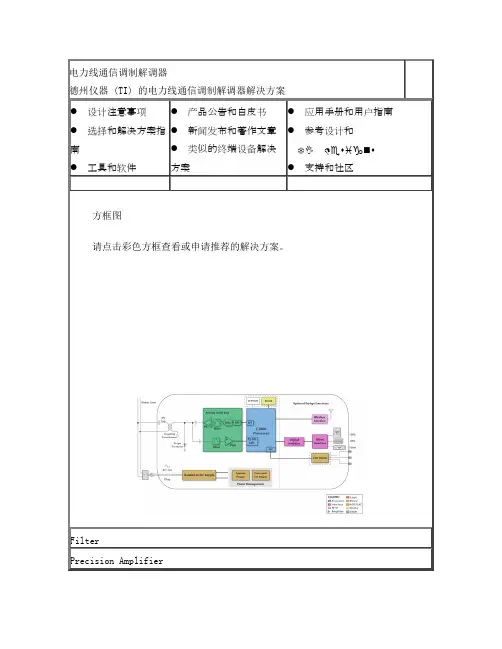
电力线通信调制解调器德州仪器 (TI) 的电力线通信调制解调器解决方案● 设计注意事项 ● 选择和解决方案指南● 工具和软件 ● 产品公告和白皮书● 新闻发布和著作文章● 类似的终端设备解决方案● 应用手册和用户指南● 参考设计和❆✋ ♏♦♓♑⏹♦● 支持和社区方框图请点击彩色方框查看或申请推荐的解决方案。
FilterPrecision Amplifier或单击彩色块以查看/申请订购推荐解决方案的样片。
电力线通信 (PLC) 利用现有电力线基础设施,为在许多工业应用引进智能监控和控制提供了经济高效的方法。
它让 PLC 成为用于智能电网应用(如智能抄表、照明控制、太阳能、插入式电动车以及家庭和楼宇中的供暖、空调和安全系统)的首选技术之一。
对这些应用实施低频窄带 PLC (LF NB PLC) 技术将提供最适合的带宽、功耗和成本要求。
在窄带域(频率高达 500kHz)运行可确保数据完整性,同时可将系统成本降到最低。
数据速率从 1.2kbps 到数百 kbps 不等,具体取决于现有标准。
开发高效 PLC 实施也会遇到困难。
电力线本身就具有噪声,因此需要强大架构才能确保数据可靠性。
此外,每种应用和工作环境都不同,需要开发人员针对各种因素优化设计。
由于协议标准和调制方案多种多样,开发人员需要灵活的开发平台,以简化设计、实现对环境条件的优化、遵守当地法规的同时可轻松调整以满足不断发展的标准。
电力线通信调制解调器系统的调制信号首先进入接收器级或有源带通滤波器,其中为滤波器选择的运算放大器应该提供低噪声、低谐波失真和低输入偏置(如 TI 的 OPA365 或 OPA353 中所示)。
使用可编程增益放大器 (PGA)(如 PGA112)调节接收信号时,可实现宽动态范围和优化信号处理。
它需要足够快速准确地连接至模数转换器的输入,以便正确转换为数字形式供处理。
这可通过 F28235 Delfino? 或F2802x/03x Piccolo? 微处理器(可升级 C2000? 32 位微处理器 (MCU) 系列的成员)的片上 12 位 ADC 来实现。
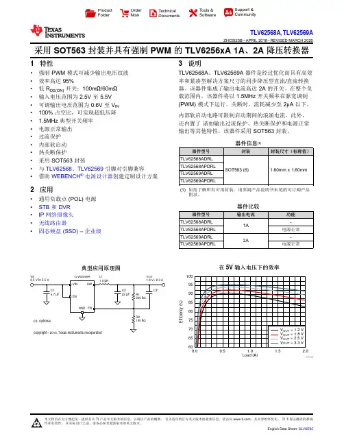
Load (A)E f f i c i e n c y (%)0.00.51.0 1.52.06065707580859095100D008V INV OUTL1TLV62569AProduct Folder Order Now Technical Documents Tools &SoftwareSupport &CommunityTLV62568A ,TLV62569AZHCSI23B –APRIL 2018–REVISED MARCH 2020采用SOT563封装并具有强制PWM 的TLV6256xA 1A 、2A 降压转换器1特性•强制PWM 模式可减少输出电压纹波•效率高达95%•低R DS(ON)开关:100m Ω/60m Ω•输入电压范围为2.5V 至5.5V •可调输出电压范围为0.6V 至V IN •100%占空比,可实现超低压降• 1.5MHz 典型开关频率•电源正常输出•过流保护•内部软启动•热关断保护•采用SOT563封装•与TLV62568、TLV62569引脚对引脚兼容•借助WEBENCH ®电源设计器创建定制设计方案2应用•通用负载点(POL)电源•STB 和DVR •IP 网络摄像头•无线路由器•固态硬盘(SSD)–企业级3说明TLV62568A 、TLV62569A 器件是经过优化而具有高效率和紧凑型解决方案尺寸的同步降压型直流/直流转换器。
该器件集成了输出电流高达2A 的开关。
在整个负载范围内,该器件将以1.5MHz 开关频率在脉宽调制(PWM)模式下运行。
关断时,流耗减少至2μA 以下。
内部软启动电路可限制启动期间的浪涌电流。
此外,还内置了诸如输出过流保护、热关断保护和电源正常输出等其他特性。
该器件采用SOT563封装。
器件信息(1)器件型号封装封装尺寸(标称值)TLV62568ADRL SOT563(6)1.60mm x 1.60mmTLV62568APDRL TLV62569ADRL TLV62569APDRL(1)如需了解所有可用封装,请参阅产品说明书末尾的可订购产品附录。
General DescriptionThe MAX4372 low-cost, precision, high-side current-sense amplifier is available in a tiny, space-saving SOT23 5-pin package. Offered in three gain versions (T = 20V/V, F = 50V/V, and H = 100V/V), this device oper-ates from a single 2.7V to 28V supply and consumes only 30μA. It features a voltage output that eliminates the need for gain-setting resistors and is ideal for today’s notebook computers, cell phones, and other systems where battery/ DC current monitoring is critical.High-side current monitoring is especially useful in bat-tery-powered systems since it does not interfere with the ground path of the battery charger. The input common-mode range of 0 to 28V is independent of the supply volt-age and ensures that the current-sense feedback remains viable even when connected to a 2-cell battery pack in deep discharge.The user can set the full-scale current reading by choos-ing the device (T, F, or H) with the desired voltage gain and selecting the appropriate external sense resistor. This capability offers a high level of integration and flex-ibility, resulting in a simple and compact current-sense solution. For higher bandwidth applications, refer to the MAX4173T/F/H data sheet.Applications●Power-Management Systems●General-System/Board-Level Current Monitoring●Notebook Computers●Portable/Battery-Powered Systems●Smart-Battery Packs/Chargers●Cell Phones●Precision-Current Sources Features●Low-Cost, Compact Current-Sense Solution●30μA Supply Current● 2.7V to 28V Operating Supply●0.18% Full-Scale Accuracy●0.3mV Input Offset Voltage●Low 1.5Ω Output Impedance●Three Gain Versions Available• 20V/V (MAX4372T)• 50V/V (MAX4372F)• 100V/V (MAX4372H)●High Accuracy +2V to +28V Common-Mode Range,Functional Down to 0V, Independent of SupplyVoltage●Available in a Space-Saving 5-Pin SOT23 Packageand 3 x 2 UCSP™ (1mm x 1.5mm) Package Ordering Information appears at end of data sheet.UCSP is a trademark of Maxim Integrated Products, Inc.19-1548; Rev 5; 5/11+Denotes lead(Pb)-free/RoHS-compliant package.T = Tape and reel.*Note: Gain values are as follows: 20V/V for the T version,50V/V for the F version, and 100V/V for the H version. Current-Sense Amplifier with Voltage OutputPin ConfigurationsOrdering InformationPARTTEMPRANGEPIN-PACKAGETOPMARK MAX4372T EUK+T-40°C to +85°C 5 SOT23ADIU MAX4372TESA+-40°C to +85°C8 SO—MAX4372TEBT+T-40°C to +85°C 3 x 2 UCSP ACXV CC , RS+, RS- to GND .........................................-0.3V to +30V OUT to GND ..........................................................-0.3V to +15V Differential Input Voltage (V RS+ - V RS-) .............................±0.3V Current into Any Pin .........................................................±10mA Continuous Power Dissipation (T A = +70°C)5-Pin SOT23 (derate 3.9mW/°C above +70°C) .......312.6mW 8-Pin SO (derate 7.4mW/°C above +70°C) ..............588.2mW 3 x 2 UCSP (derate 3.4mW/°C above +70°C) .........273.2mWOperating Temperature Range ...........................-40°C to +85°C Storage Temperature Range ............................-65°C to +150°C Lead Temperature (soldering, 10s) .................................+300°C Soldering Temperature (reflow) .......................................+260°C(V RS+ = 0 to 28V, V CC = 2.7V to 28V, V SENSE = 0V, R LOAD = 1MΩ, T A = T MIN to T MAX , unless otherwise noted. Typical values are at T A = +25°C.) (Note 1)Current-Sense Amplifier with Voltage OutputAbsolute Maximum RatingsStresses beyond those listed under “Absolute Maximum Ratings” may cause permanent damage to the device. These are stress ratings only, and functional operation of the device at these or any other conditions beyond those indicated in the operational sections of the specifications is not implied. Exposure to absolute maximum rating conditions for extended periods may affect device reliability.Electrical CharacteristicsPARAMETERSYMBOL CONDITIONSMIN TYPMAX UNITS Operating Voltage Range (Note 2)V CC 2.728V Common-Mode Input Range (Note 3)V CMR 028V Common-Mode Rejection CMR V RS+ > 2V85dB Supply Current I CC V RS+ > 2V, V SENSE = 5mV 3060μA Leakage CurrentI RS+, I RS-V CC = 0V, V RS+ = 28V 0.051.2μAInput Bias CurrentI RS+V RS+ > 2V 01μAV RS+ ≤ 2V -25+2I RS-V RS+ > 2V 02V RS+ ≤ 2V-50+2Full-Scale Sense Voltage (Note 4)V SENSEGain = 20V/V or 50V/V 150mV Gain = 100V/V 100Input Offset Voltage (Note 5)V OST A = +25°CV CC = V RS+ = 12V MAX4372_ESA 0.3±0.8mVMAX4372_EUK, _EBT 0.3±1.3T A = T MIN to T MAX V CC = V RS+ = 12VMAX4372_ESA ±1.1MAX4372_EUK, _EBT±1.9Full-Scale Accuracy (Note 5)V SENSE = 100mV, V CC = 12V,V RS+ = 12V, T A = +25°C (Note 7)±0.18±3%Total OUT Voltage Error (Note 6)V SENSE = 100mV, V CC = 12V,V RS+ = 12V (Note 7)±6V SENSE = 100mV, V CC = 28V,V RS+ = 28V (Note 7)±0.15±7V SENSE = 100mV, V CC = 12V,V RS+ = 0.1V (Note 7)±1±28V SENSE = 6.25mV, V CC = 12V,V RS+ = 12V (Note 8)±0.15(V RS+ = 0 to 28V, V CC = 2.7V to 28V, V SENSE = 0V, R LOAD = 1MΩ, T A = T MIN to T MAX , unless otherwise noted. Typical values are at T A = +25°C.) (Note 1)Note 1: All devices are 100% production tested at T A = +25°C. All temperature limits are guaranteed by design.Note 2: Guaranteed by PSR test.Note 3: Guaranteed by OUT voltage error test.Note 4: Output voltage is internally clamped not to exceed 12V.Note 5: V OS is extrapolated from the gain accuracy tests.Note 6: Total OUT voltage error is the sum of gain and offset voltage errors.Note 7: Measured at I OUT = -500μA (R LOAD = 4kΩ for gain = 20V/V, R LOAD = 10kΩ for gain = 50V/V, R LOAD = 20kΩ for gain = 100V/V).Note 8: 6.25mV = 1/16 of 100mV full-scale voltage (C/16).Note 9: The device does not reverse phase when overdriven.Current-Sense Amplifier with Voltage OutputElectrical Characteristics (continued)PARAMETERSYMBOL CONDITIONSMINTYP MAXUNITSOUT Low Voltage(MAX4372T, MAX4372F)V OLV CC = 2.7V,V SENSE = -10mV, V RS+ = 28V I OUT = 10μA 2.6mVI OUT = 100μA 965OUT Low Voltage (MAX4372H)V OLV CC = 2.7V,V SENSE = -10mV, V RS+ = 12VI OUT = 10μA 2.6mVI OUT = 100μA965OUT High VoltageV CC - V OHV CC = 2.7V, I OUT = -500μA, V SENSE = 250mV, V RS+ = 28V0.10.25V-3dB Bandwidth BWV RS+ = 12V,V CC = 12V,C LOAD = 10pFV SENSE = 20mV,gain = 20V/V275kHzV SENSE = 20mV,gain = 50V/V 200V SENSE = 20mV,gain = 100V/V 110V SENSE = 6.25mV50GainMAX4372T20V/VMAX4372F 50MAX4372H100Gain AccuracyV SENSE = 20mV to 100mV, V R S + = 12V T A = +25°C ±0.25±2.5%T A = -40°C to +85°C ±5.5OUT Settling Time to 1% of Final ValueGain = 20V/V, V CC = 12V, V RS+ = 12V, C LOAD = 10pFV SENSE = 6.25mV to 100mV20µsV SENSE = 100mV to 6.25mV20Capacitive-Load Stability No sustained oscillations1000pF OUT Output Resistance R OUT V SENSE = 100mV 1.5ΩPower-Supply Rejection PSRV OUT = 2V, V RS+ > 2V7585dB Power-Up Time to 1% of Final ValueV CC = 12V, V RS+ = 12V,V SENSE = 100mV, C LOAD = 10pF 0.5ms Saturation Recovery Time (Note 9)V CC = 12V, V RS+ = 12V, C LOAD = 10pF0.1ms(V CC = 12V, V RS+ = 12V, V SENSE = 100mV, T A = +25°C, unless otherwise noted.)Current-Sense Amplifier with Voltage OutputTypical Operating Characteristics25.027.530.032.535.0SUPPLY CURRENT vs. SUPPLY VOLTAGESUPPLY VOLTAGE (V)S U P P L Y C U R R E N T (µA )121648202428-1.2-0.8-1.0-0.2-0.4-0.60.40.200.6010515202530TOTAL OUTPUT ERROR vs. SUPPLY VOLTAGESUPPLY VOLTAGE (V)O U T P U T E R R O R (%)00.20.40.60.81.01.21.41.610515202530TOTAL OUTPUT ERROR vs. COMMON-MODE VOLTAGECOMMON-MODE VOLTAGE (V)O U T P U T E R R O R (%)510152025303540-401060-153585SUPPLY CURRENT vs. TEMPERATURETEMPERATURE (°C)S U P P L Y C U R R E N T (µA )-1.0-0.50.501.01.5010050150200250300TOTAL OUTPUT ERROR vs. V SENSEV SENSE (mV)O U T P U T E R R O R (%)-1.0-0.9-0.8-0.7-0.6-0.5-0.4-0.3-0.2-0.10GAIN ACCURACY vs. TEMPERATURETEMPERATURE (°C)G A I N A C C U R A C Y (%)-401060-15358528.029.028.530.029.531.531.030.532.0SUPPLY CURRENTvs. COMMON-MODE VOLTAGECOMMON-MODE VOLTAGE (V)S U P P L Y C U R R E N T (µA )-45-90100100k10k 1k POWER-SUPPLY REJECTIONvs. FREQUENCY-75-85-55-65-40-70-80-50-60M A X 4372T t o c 06FREQUENCY (Hz)P S R (d B )-1.0-0.8-0.6-0.4-0.200.20.40.60.81.0-401060-153585TOTAL OUTPUT ERROR vs. TEMPERATURETEMPERATURE (°C)T O T A L O U T P U T E R R O R (%)(V CC = 12V, V RS+ = 12V, V SENSE = 100mV, T A = +25°C, unless otherwise noted.)Current-Sense Amplifier with Voltage OutputTypical Operating Characteristics (continued)V OUTV SENSE600mV200mV30mV10mV MAX4372TSMALL-SIGNAL TRANSIENT RESPONSEMAX4372T toc1020µs/div V OUTV SENSE1V3V50mV 150mV MAX4372TLARGE-SIGNAL TRANSIENT RESPONSEMAX4372T toc1320µs/divV OUTV SENSE 010V0100mV MAX4372HLARGE-SIGNAL TRANSIENT RESPONSE20µs/divMAX4372T toc15V OUTV SENSE2.5V7.5V50mV 150mVMAX4372FLARGE-SIGNAL TRANSIENT RESPONSE20µs/divMAX4372T toc143-81k100k10k1MSMALL-SIGNAL GAIN vs. FREQUENCY-7FREQUENCY (Hz)G A I N (d B)-6-5-4-3-2-1012V OUTV SENSE 1.5V0.5V30mV 10mVMAX4372FSMALL-SIGNAL TRANSIENT RESPONSEMAX4372T toc1120µs/div V OUTV SENSE 3V1V30mV10mV MAX4372HSMALL-SIGNAL TRANSIENT RESPONSEMAX4372T toc1220µs/divDetailed DescriptionThe MAX4372 high-side current-sense amplifier features a 0 to 28V input common-mode range that is indepen-dent of supply voltage. This feature allows the monitoring of current flow out of a battery in deep discharge, and also enables high-side current sensing at voltages far in excess of the supply voltage (V CC).Current flows through the sense resistor, generating a sense voltage (Figure 1. Functional Diagram). Since A1’s inverting input is high impedance, the voltage on the negative terminal equals V IN - V SENSE. A1 forces its positive terminal to match its negative terminal; therefore, the voltage across R G1 (V IN - V1-) equals V SENSE. This creates a current to flow through R G1 equal to V SENSE/ R G1. The transistor and current mirror amplify the current by a factor of β. This makes the current flowing out of the current mirror equal to:I M = β V SENSE/R G1A2’s positive terminal presents high impedance, so this current flows through R GD, with the following result:V2+ = R GD β x V SENSE/R G1R1 and R2 set the closed-loop gain for A2, which ampli-fies V2+, yielding:V OUT = R GD x β x V SENSE/R G1 (1 + R2/R1)The gain of the device equals:OUT SEN G1SE RGD x (1 + R2/R1)V V/Rβ=Applications Information Recommended Component ValuesThe MAX4372 operates over a wide variety of current ranges with different sense resistors. Table 1 lists com-mon resistor values for typical operation of the MAX4372.Choosing R SENSEGiven the gain and maximum load current, select R SENSE such that V OUT does not exceed V CC - 0.25V or 10V. To measure lower currents more accurately, use a high value for R SENSE. A higher value develops a higher sense volt-age, which overcomes offset voltage errors of the internal current amplifier.In applications monitoring very high current, ensure R SENSE is able to dissipate its own I2R losses. If the resistor’s rated power dissipation is exceeded, its value may drift or it may fail altogether, causing a differential voltage across the terminals in excess of the absolute maximum ratings.Figure 1. Functional DiagramCurrent-Sense Amplifier with Voltage OutputPin/Bump DescriptionPIN BUMPNAME FUNCTIONSOT23SO UCSP13A2GND Ground24A3OUT Output Voltage. V OUT is proportional to the magnitude of V SENSE (V RS+ - V RS-).31A1V CC Supply Voltage. Use at least a 0.1μF capacitor to decouple V CC from fast transients.48B1RS+Power Connection to the External Sense Resistor56B3RS-Load-Side Connection to the External Sense Resistor —2, 5, 7—N.C.No Connection. Not internally connected.Using a PC Board Trace as R SENSEIf the cost of R SENSE is an issue and accuracy is not criti-cal, use the alternative solution shown in Figure 2. This solution uses copper PC board traces to create a sense resistor. The resistivity of a 0.1in wide trace of 2oz copper is about 30mΩ/ft. The resistance temperature coefficient of copper is fairly high (approximately 0.4%/°C), so sys-tems that experience a wide temperature variance must compensate for this effect. In addition, self-heating intro-duces a nonlinearity error. Do not exceed the maximum power dissipation of the copper trace.For example, the MAX4372T (with a maximum load cur-rent of 10A and an R SENSE of 5mΩ) creates a full-scale V SENSE of 50mV that yields a maximum V OUT of 1V. R SENSE, in this case, requires about 2in of 0.1in wide copper trace.UCSP Applications InformationFor the latest application details on UCSP construction, dimensions, tape carrier information, printed circuit board techniques, bump-pad layout, and recommended reflow temperature profile, as well as the latest information on reliability testing results, go to the Maxim’s website at /ucsp to find the Application Note: UCSP—A Wafer-Level Chip-Scale Package.Figure 2. Connections Showing Use of PC BoardTable 1. Recommended Component ValuesCurrent-Sense Amplifier with Voltage OutputFULL-SCALE LOAD CURRENT,I LOAD (A)CURRENT-SENSERESISTOR,R SENSE (mΩ)GAIN(V/V)FULL-SCALE OUTPUTVOLTAGE (FULL-SCALEV SENSE = 100mV),V OUT (V)0.1100020 2.0 50 5.0 10010.0110020 2.0 50 5.0 10010.052020 2.0 50 5.0 10010.0101020 2.0 50 5.0 10010.0Current-Sense Amplifier with Voltage Output Ordering Information (continued)Pin Configurations (continued)PARTTEMPRANGEPIN-PACKAGETOPMARKMAX4372F EUK+T-40°C to +85°C 5 SOT23ADIV MAX4372FESA+-40°C to +85°C8 SO—MAX4372FEBT+T-40°C to +85°C 3 x 2 UCSP ACX MAX4372H EUK+T-40°C to +85°C 5 SOT23ADIW MAX4372HESA+-40°C to +85°C8 SO—MAX4372HEBT+T-40°C to +85°C 3 x 2 UCSP ACZChip InformationPROCESS: BiCMOS+Denotes lead(Pb)-free/RoHS-compliant package. T = Tape and reel.Current-Sense Amplifier with Voltage Output Package InformationFor the latest package outline information and land patterns (footprints), go to /packages. Note that a “+”, “#”, or “-” in the package code indicates RoHS status only. Package drawings may show a different suffix character, but the drawing pertains to the package regardless of RoHS status.PACKAGE TYPE PACKAGE CODE OUTLINE ND PATTERN NO.5 SOT23U5+121-005790-01748 SO S8+221-004190-00965 UCSP B6+221-0097—Note: MAX4372_EBT uses package code B6-2.Current-Sense Amplifier with Voltage Output Package Information (continued)For the latest package outline information and land patterns (footprints), go to /packages. Note that a “+”, “#”, or “-” in the package code indicates RoHS status only. Package drawings may show a different suffix character, but the drawing pertains to the package regardless of RoHS status.Current-Sense Amplifier with Voltage Output Package Information (continued)For the latest package outline information and land patterns (footprints), go to /packages. Note that a “+”, “#”, or “-” in the package code indicates RoHS status only. Package drawings may show a different suffix character, but the drawing pertains to the package regardless of RoHS status. Maxim Integrated │11Maxim Integrated cannot assume responsibility for use of any circuitry other than circuitry entirely embodied in a Maxim Integrated product. No circuit patent licenses are implied. Maxim Integrated reserves the right to change the circuitry and specifications without notice at any time. The parametric values (min and max limits) shown in the Electrical Characteristics table are guaranteed. Other parametric values quoted in this data sheet are provided for guidance.Maxim Integrated and the Maxim Integrated logo are trademarks of Maxim Integrated Products, Inc.Current-Sense Amplifier with Voltage Output© 2011 Maxim Integrated Products, Inc. │ 12Revision HistoryREVISIONNUMBERREVISION DATE DESCRIPTION PAGES CHANGED 47/09Updated feature in accordance with actual performance of the product 155/11Updated V RST conditions to synchronize with tested material and addedlead-free designation 1–3, 8For pricing, delivery, and ordering information, please contact Maxim Direct at 1-888-629-4642, or visit Maxim Integrated’s website at .。
Evaluates: MAX16826MAX16826 Evaluation KitGeneral DescriptionThe MAX16826 evaluation kit (EV kit) provides a proven design to evaluate the MAX16826, a four-string, I 2C programmable high-brightness LED (HB LED) driver with PWM dimming control. The EV kit also includes Windows ® 2000/XP/Vista ®-compatible software that pro-vides a simple graphical user interface (GUI) for exercis-ing the features of the MAX16826. The MAX16826 EV kit PCB comes with a MAX16826ATJ+ installed. The EV kit is configured in a boost application.This EV kit can be modified by changing component val -ues on the board for other configurations (including RGB LED applications). Refer to the MAX16826 IC data sheet for more information.Features●Four Independently Controllable LED Strings ●7 LEDs Per String Configuration●Independently Programmable 50mA to 150mAString Current●7.5V to 22V Input Voltage●Can Withstand Automotive Load Dump Up to 40Vfor 400ms●0% to 100% DIM Duty Cycle Range ●Shorted LED Protection and Detection ●Open LED String Detection●Adaptive Boost-Stage Voltage Optimization●Convenient Breakaway LED Driver Board EasilyAdaptable to End Application ●Low Mechanical Profile●Windows 2000/XP/Vista (32-Bit)-Compatible Software ●USB-PC Interface●USB-to-I 2C On-Board Circuitry ●Fully Assembled and Tested ●Lead-Free and RoHS Compliant19-4271; Rev 1; 12/20Windows and Windows Vista are registered trademarks of Microsoft Corp.+Denotes lead-free and RoHS compliant.#Denotes RoHS compliant.PARAMETERDESCRIPTION Configuration 7 white LEDs/stringNumber of Strings4 strings LED Current Adjustment Range 50mA to 150mATotal Maximum LED Power 16.8W V IN (min)7.5V V IN (max)22V Load Dump40V for < 400ms Nominal Boost Voltage Adjustment Range22.4V to 32VNominal OVP Trip Threshold 35V Boost Stage Switching Frequency350kHzPARTTYPE MAX16826EVKIT+EV Kit MAX16826EVKIT#EV KitDESIGNATION QTY DESCRIPTIONC1, C2, C3, C5–C8, C12, C15,C17, C23, C2412100nF ±10%, 16V X7R ceramic capacitors (0603)TDK C1608X7R1C104K C9133nF ±10%, 50V X7R ceramic capacitor (0603)TDK C1608X7R1H333K C10, C11222pF ±5%, 50V C0G ceramic capacitors (0603)TDK C1608C0G1H220J C13, C14,C18–C2161μF ±10%, 16V X7R ceramic capacitors (0603)TDK C1608X7R1C105K C16, C25210μF ±10%, 10V X5R ceramic capacitors (1210)Murata GRM32FR61A106KDESIGNATION QTY DESCRIPTIONC26, C28210μF ±20%, 50V X5R ceramic capacitors (2220)Murata GRM55DR61H106K C27110μF ±20%, 50V X7S ceramic capacitor (1210)Taiyo Yuden UMK325BJ106MM-T C2912.2nF ±5%, 50V C0G ceramic capacitor (0603)Murata GRM1885C1H222K C3011μF ±10%, 50V X7R ceramic capacitor (1210)Murata GRM32RR71H105K C3214.7μF ±10%, 6.3V X5R ceramic capacitor (0603)Murata GRM188R60J475KLED Driver Board SpecificationOrdering InformationComponent ListClick here to ask about the production status of specific part numbers.DESIGNATION QTY DESCRIPTIONC3312200pF ±10%, 50V X7R ceramic capacitor (0402)Murata GRM155R71H222KC34, C35247μF ±20%, 50V electrolytic capacitorsPanasonic EEE-FK1H470XPC36, C370Not installed, capacitors (0603)C3811000pF ±5%, 50V C0G ceramic capacitor (0402)Murata GRM1555C1H102JA01DC391220pF ±5%, 50V C0G ceramic capacitor (0402)Murata GRM1555C1H221JC401100pF ±5%, 50V C0G ceramic capacitor (0402)Murata GRM1555C1H101JC41–C4440.01μF ±10%, 50V X7R ceramic capacitors (0402)Murata GRM155R71H103KC450Not installed, capacitor (0402)D1160V, 1A Schottky diode (SMB) Diodes, Inc. B160B-13-FJ11USB series-B right-angle PC-mount receptacleJ2, J30Not installed JU2–JU873-pin headersL11Ferrite bead (0603) TDK MMZ1608R301AL2122μH ±20%, 5A, 52mΩ inductor Coilcraft MSS1260-223MlLED11Red LED (0603) Panasonic LNJ208R8ARAP1, P22Connectors, FFC/FPC 18-pos, 1mm P31Connector, FFC/FPC 6-pos, 1mmQ1140V, 9A, 2.5W n-channel MOSFET (8 SO)International Rectifier IRF7469Q2–Q5455V, 1.9A, 160mΩ n-channel MOSFET s (SOT223) International Rectifier IRFL014NPbFR11220Ω ±5% resistor (0603)R21 2.2kΩ ±5% resistor (0603)R3, R9, R103 1.5kΩ ±5% resistors (0603) R4, R5227Ω ±5% resistors (0603)R61470Ω ±5% resistor (0603)R71100kΩ ±5% resistor (0603)R817.5kΩ ±1% resistor (0603)R11168Ω ±1%, 0.25W resistor (1206)DESIGNATION QTY DESCRIPTION R1210.04Ω ±1%, 0.5W sense resistor(2010)Vishay/Dale WSL2010R0400FEA R131215kΩ ±1% resistor (0402) R14, R16210kΩ ±1% resistors (0402) R151249kΩ ±1% resistor (0402)R171 1.27kΩ ±1% resistor (0603)R181182kΩ ±1% resistor (0603)R1912kΩ ±1% resistor (0402) R20, R22,R24, R264100kΩ ±1% resistors (0402) R21, R23,R25, R27416.5kΩ ±1% resistors (0402) R28–R3142.2Ω ±1%, 100mW sense resistors(0603)Panasonic ECG ERJ-3RQF2R2V R32, R3320Ω ±5% resistors (0603)R34–R3740Ω ±5% resistors (0402)R38112.1Ω ±1% resistor (0805)R391470Ω ±5% resistor (0402)R40110kΩ ±5% resistor (0603) R41–R444237kΩ ±1% resistors (0603) U11LED driver (32 TQFN)Maxim MAX16826ATJ+ U2, U82Microcontrollers (68 QFN-EP*)Maxim MAXQ2000-RAX+ U31UART-to-USB converter (32 TQFP)FTDI FT232BLU4193C46A 3-wire EEPROM (8 SO)Atmel AT93C46A-10SU-2.7 U51p-channel MOSFET power switch(8 SO)Maxim MAX890LESA+U61LDO regulator (5 SC70)Maxim MAX8511EXK25+T U71LDO regulator (5 SC70)Maxim MAX8511EXK33+T Y1120MHz crystal oscillatorY216MHz crystalHong Kong X’talsSSL6000000E18FAF—1Cable, flat flex 18-position, 1mm, 5in—7Shunts—1USB high-speed A-to-B cable,5ft (1.5m)—1PCB: MAX16828 Evaluation Kit+Component List (continued)*Exposed pad.Quick StartRecommended EquipmentBefore beginning, the following equipment is needed: ●MAX16826 EV kit (USB cable included)● A user-supplied Windows 2000/XP/Vista PC with a spare USB port●7V to 24V, 5A DC power supply●Four strings of white LEDs (7 LEDs/string)Note: In the following sections, software-related items are identified by bolding. Text in bold refers to items directly from the EV kit software. Text in bold and underlined refers to items from the Windows operating systemProcedureThe MAX16826 EV kit is fully assembled and tested. Follow the steps below to verify board operation:1) Visit /evkitsoftware to down-load the latest version of the EV kit software,16826Rxx.ZIP (xx in the filename denotes the soft -ware version number). Save the EV kit software to a temporary folder and uncompress the ZIP file.2) Install the EV kit software on your computer by run -ning the INSTALL.EXE program inside the temporary folder. The program files are copied and icons are created in the Windows Start | Programs menu.3) Verify that all jumpers (JU2–JU8) are in their defaultpositions, as shown in Table 1.4) Connect the USB cable from the PC to the EV kitboard. A New Hardware Found window pops up when installing the USB driver for the first time. If you do not see a window that is similar to the one described above after 30 seconds, remove the USB cable from the board and reconnect it. Administra-tor privileges are required to install the USB device driver on Windows.5) Follow the directions of the Add New HardwareWizard to install the USB device driver. Choose the Search for the best driver for your device option. Specify the location of the device driver to be C:\Program Files\MAX16826 (default installation direc-tory) using the Browse button. During device driver installation, Windows may show a warning message indicating that the device driver Maxim uses does not contain a digital signature. This is not an error condi-tion and it is safe to proceed with installation. Refer to the USB_Driver_Help.PDF document included with the software for additional information.6) Set the output of the power supply to 12V. Turn offthe power supply.7) Connect the positive terminal of the power supply tothe VIN pad of the LED driver board.Note: Indicate that you are using the MAX16826 when contacting these component suppliers.SUPPLIERPHONE WEBSITECoilcraft, Diodes, Inc.Hong Kong X’tals Ltd.852-******** International RectifierMurata Electronics North America, Panasonic Taiyo Yuden TDK Vishay/Dale402-563-6866FILE DESCRIPTIONINSTALL.EXE Installs the EV kit files on your computerMAX16826.EXE Application program FTDIBUS.INF USB device driver file FTDIPORT.INF VCP device driver file UNINST.INI Uninstalls the EV kit software USB_Driver_Help.PDFUSB driver installation help fileComponent SuppliersMAX16826 EV Kit Files8) Connect the negative terminal of the power supply tothe PGND pad of the LED driver board.9) Ensure that the supplied ribbon cable is firmly con -nected to the P1 and P2 connectors.10) Connect the anode ends of the LED strings to theP3-1 pin of the P3 connector.11) Connect the cathode ends of the LED strings to theP3-2 to P3-5 pins of the P3 connector.12) Turn on the power supply13) Start the MAX16826 EV kit software by opening itsicon in the Start | Programs menu. The EV kit soft-ware main window appears, as shown in Figure 1.14) Press the Start button to start the LED driver.15) Verify that all of the LEDs are lit.Table 1. MAX16826 EV Kit Jumper Descriptions (JU2–JU8)*Default position.JUMPER SHUNT POSITIONDESCRIPTIONJU21-2*On-board PWM signal for Ch12-3Connect user-supplied PWM signal for Ch1 to the on-board DIM1 pad JU31-2*On-board PWM signal for Ch22-3Connect user-supplied PWM signal for Ch2 to the on-board DIM2 pad JU41-2*MAX16826 SDA signal connected to on-board microcontroller 2-3Connect user-supplied SDA signal to the on-board SDA pad JU51-2*MAX16826 SCL signal connected to on-board microcontroller 2-3Connect user-supplied SCL signal to the on-board SCL pad JU61-2*MAX16826 SYNC/EN signal connected to on-board microcontroller 2-3Connect user-supplied SYNC/EN signal to the on-board SYNC/EN pad JU71-2*On-board PWM signal for Ch32-3Connect user-supplied PWM signal for Ch3 to the on-board DIM3 pad JU81-2*On-board PWM signal for Ch42-3Connect user-supplied PWM signal for Ch4 to the on-board DIM4 padDetailed Description of SoftwareThe MAX16826 evaluation kit software has all the functions to evaluate the MAX16826 IC. To start the MAX16826 EV kit software, click Start | Programs | Maxim MAX16826 Evaluation Kit | Maxim MAX16826 Evaluation Kit that is created during installation. The GUI main window appears as shown in Figure 1.Figure 1. MAX16826 EV Kit Software Main WindowString Current SetThe String Current Set group box is located at the upperleft corner of the main window. Use the scrollbars toadjust the current of the LED strings. The correspondingvalues of the current will be shown in the adjacent editboxes. Press the Read button to read the values from thelinear regulator output registers of the MAX16826. Theequivalent values of the output current will be shown inthe edit boxes.Boost Output ControlThe Boost Output Control Mode group box has thefunctions to control the boost output voltage.To control the boost output voltage manually, click on theradio button next to the Manual Control group box. Usethe scrollbar to adjust the output voltage, and the volt-age value will be displayed in the adjacent edit box. Theactual boost output voltage can be seen in the Read BackValues group box.To use the software automatic control, click on the radiobutton next to the Software Control group box. The editbox next to the Set button is used to change the Drain toGND regulated voltage of the current sink FETs on the LEDstring with the highest voltage drop. This voltage setting willdepend on how much overhead the user is willing to have.If the set value is too low, the LED currents will no longerbe well regulated and may indeed drop because the boostvoltage might fall too low. The scrollbar in this mode willmove automatically to compensate and regulate the outputvoltage. The update rate is approximately once per second.In any case, the channel with the lowest voltage across thesink FET will be regulated to the value in the edit box. DIM Pulse Width Modulation (DPWM)The DPWM group box is located at the center of the mainwindow. The four DIM PWM signals generated by theon-board MAXQ2000 microcontrollers are used to controlthe brightness of the LEDs. Adjust the scrollbars in theDPWM Duty Cycle group box to change the duty cycles of the PWM signals and the values of the duty cycle (%)are shown in the adjacent edit boxes. Check the Set AllChannels to 100% Duty Cycle checkbox to force all channel duty cycles to 100%.In the DPWM Frequency group box, change the DPWMfrequency by adjusting the scrollbar position and pressthe Set button. The frequency value will be shown in theedit box.To guarantee that the leading edge of all the DIM signalsare synchronized, press the Set button in the DPWMFrequency group box.Press the Start button to start to generate the PWM signals.Press the Stop button to stop all PWM signals.StatusThe Status group box is located at the right of the main window. The software reads the external FET drain voltage measurements, and the boost output voltage measurement from the ADC output registers of the MAX16826. The software multiplies the measured values by the appropriate scaling factor and then displays them in the Read Back Values group box.Enter the values into the edit boxes in the Fault Level Set group box to set the fault-detection values. When the value in the Read Back Values group box is less than the fault-detection value, then the color of the read-back value changes to dark green. When the read-back value is 0 to 10% higher than the fault-detection value, the read-back value turns a lime color. If the read-back value is more than 10% higher than the fault-detection value, then the read-back value turns purple. The read-back value turns red when it is more than 20% higher than the fault-detection value.The software also reads the fault register to detect the fault conditions. If a fault condition exists, it will be shown in the String Fault Status group box. See Table 2 for the fault-condition explanations.Press the Read button to update the Status group box. By checking the Automatic Read checkbox, the Status group box will be automatically updated every second. Enable/DisableThe Enable/Disable group box controls the signal on the SYNC/EN pin. Click on the Enable radio button to set the signal high and enable the MAX16826. Click on the Disable radio button to set the signal low and disable the MAX16826.StandbyCheck the Standby checkbox to set the MAX16826 to standby mode. Refer to the MAX16826 IC data sheet for more information regarding standby mode.Table 2. Fault Conditions*Open LED string detection may require multiple flag examination. FAULT NAME CONDITIONTOADC conversion timeout; alsocorresponds to open string condition* Open LED string openShort LED string shortedOVP OvervoltageScaling FactorsThe calculations for the LED string current, boost output voltage, and the read-back values are based on the scal-ing factors. You can change the scaling factor by select-ing the Scaling Factor menu item under the Scaling Factors menu bar. In the pop-up window shown in Figure 2, enter the appropriate scaling factor.See Table 3 for the formulas for the scaling factors. These values can be used for calibration against actual read values with external instruments.When the default values are changed, they are stored in the software. Re-enter the default values to bring the software back to the default setting.Table 3. Scaling FactorFigure 2. Scaling Factor WindowSCALING FACTOR FORMULADEFAULTVALUE DR1 (ADC read-back voltageacross Drain and GND for thesink FET on Ch1)1 + (R20/R21)7.046DR2 (ADC read-back voltageacross Drain and GND for thesink FET on Ch2)1 + (R22/R23)7.046DR3 (ADC read-back voltageacross Drain and GND for thesink FET on Ch3)1 + (R24/R25)7.046DR4 (ADC read-back voltageacross Drain and GND for thesink FET on Ch4)1 + (R26/R27)7.046Read Back VBoost (ADC read-back boost output voltage)1 + (R15/R16)25.900 String Current Set Ch1 (LEDstring current for Ch1)R31 2.200 String Current Set Ch2 (LEDstring current for Ch2)R30 2.200 String Current Set Ch3 (LEDstring current for Ch3)R29 2.200 String Current Set Ch4 (LEDstring current for Ch4)R28 2.200 VBoost (Boost output voltage) 1 + (R13/R14)22.500Detailed Description of HardwareThe MAX16826 EV kit board provides a proven layout for evaluating the MAX16826 IC. This EV kit consists of a controller board and an LED driver board. The break-away slots at the center of the EV kit make it easier for the user to break and separate the controller board from the LED driver board. This is done so that once the evaluation is complete with the included software, the driver board can easily be used in the target application environment with the target system microcontroller.To connect the power, ground, PWM, and the I2C inter-face signals of the boards, attach the ribbon cable to the P1 connector of the controller board and attach the other end of the ribbon cable to the P2 connector of the LED driver board.Controller BoardThe controller board acts as the bridge between the soft-ware in the PC and the actual LED driver board containing the MAX16826. In addition to the USB connectivity, it gen-erates the four adjustable PWM DIM signals that control the brightness of the LEDs. The controller board com-municates with the driver board through the I2C interface, and is able to read or change the values of the registers in the MAX16826.The user can use the MAX16826 evaluation kit software to control the controller board.See Table 1 to control the MAX16826 with a user-supplied PWM signal.LED Driver BoardThe LED driver board is able to drive up to four LED strings (7 LEDs/string). LED strings can be connected to the LED driver board through the P3 connector by using a ribbon cable. Connect all of the anode ends of the LED strings to the P3-1 pin (which connects to the boost out-put) of the P3 connector. Then connect the cathode ends of the LED strings to the P3-2 to P3-5 pins (that connects to the drains of the sink FETs) of the P3 connector. User-Supplied I2C InterfaceTo use the MAX16826 EV kit with a user-supplied I2C interface, install the shunts on pins 2-3 of JU4 and JU5. Connect SDA, SCL, and GND lines from the usersupplied I2C interface to the SDA, SCL, and PGND pads on the MAX16826 controller board.After the LED driver board has broken away from the controller board, the user may connect their supplied I2C, DIM, and power signals to the LED driver board through the P2 connector using a ribbon cable. See Table 4 for the pin description of the P2 connector.Table 4. Pin Description for P2 Connector PIN NUMBER DESCRIPTIONP2-1 to P2-5Connect to the VIN pin of the MAX16826 P2-6Not connectedP2-7 to P2-11Connect to the groundP2-12Connects to the SYNC/EN pin of theMAX16826P2-13Connects to the SDA pin of the MAX16826P2-14Connects to the SCL pin of the MAX16826P2-15Connects to the DIM4 pin of the MAX16826P2-16Connects to the DIM3 pin of the MAX16826P2-17Connects to the DIM2 pin of the MAX16826P2-18Connects to the DIM1 pin of the MAX16826Figure 3. MAX16826 EV Kit LED Driver Board SchematicFigure 4a. MAX16826 EV Kit Controller Board Schematic (Sheet 1 of 2)Figure 4b. MAX16826 EV Kit Controller Board Schematic (Sheet 2 of 2)Maxim Integrated cannot assume responsibility for use of any circuitry other than circuitry entirely embodied in a Maxim Integrated product. No circuit patent licenses are implied. Maxim Integrated reserves the right to change the circuitry and specifications without notice at any time.REVISIONNUMBERREVISION DATE DESCRIPTION PAGES CHANGED 009/08Initial release —112/20Updated Ordering Information 1Revision HistoryFor pricing, delivery, and ordering information, please visit Maxim Integrated’s online storefront at https:///en/storefront/storefront.html.。
An exclusive-OR gate has many applications,some of which can be represented better by alternative logic symbols.=1EXCLUSIVE ORThese are five equivalent exclusive-OR symbols valid for an SN74AHC1G86gate in positive logic;negation may be shown at any twoports.=2k2k +1LOGIC-IDENTITY ELEMENTEVEN-PARITY ELEMENTODD-PARITY ELEMENTThe output is active (low)if all inputs stand at the same logic level (that is,A = B).The output is active (low)if an even number of inputs (that is,0 or 2) are active.The output is active (high)if an odd number of inputs (that is,only 1of the2)areactive.Product FolderSample &BuyTechnical Documents Tools &SoftwareSupport &CommunitySN74AHC1G86SCLS323N –MARCH 1996–REVISED DECEMBER 2014SN74AHC1G86Single 2-Input Exclusive-OR Gate1Features2Applications•Operating Range of 2V to 5.5V •Cameras•Max t pd of 8ns at 5V•Programmable Logic Controllers •Low Power Consumption,10-µA Max I CC •Telecom Infrastructure •±8-mA Output Drive at 5V•Wireless Headsets•Schmitt-Trigger Action at All Inputs Makes the •Motor Drives and Controls Circuit Tolerant for Slower Input Rise and Fall •TVsTime•Set-top-boxes •Latch-Up Performance Exceeds 250mA •AudioPer JESD 17•ESD Protection Exceeds JESD 223Description–2000-V Human-Body Model The SN74AHC1G86is a single 2-input exclusive-OR gate.The device performs the Boolean function Y =A –200-V Machine Model×B or Y =+in positive logic.–1000-V Charged-Device ModelDevice Information (1)PART NUMBER PACKAGE BODY SIZE (NOM)SOT-23(5) 2.90mm x 1.60mm SN74AHC1G86SC-70(5) 2.00mm x 1.30mm SOT-553(5)1.65mm x 1.20mm(1)For all available packages,see the orderable addendum atthe end of the data sheet.4Simplified SchematicAn IMPORTANT NOTICE at the end of this data sheet addresses availability,warranty,changes,use in safety-critical applications,intellectual property matters and other important disclaimers.PRODUCTION DATA.SN74AHC1G86SCLS323N–MARCH1996–REVISED Table of Contents1Features..................................................................19Detailed Description. (8)9.1Overview (8)2Applications (1)9.2Functional Block Diagram (8)3Description (1)9.3Feature Description (8)4Simplified Schematic (1)9.4Device Functional Modes (8)5Revision History (2)10Application and Implementation (9)6Pin Configuration and Functions (3)10.1Application Information (9)7Specifications (4)10.2Typical Application (9)7.1Absolute Maximum Ratings (4)11Power Supply Recommendations (10)7.2ESD Ratings (4)12Layout (11)7.3Recommended Operating Conditions (4)12.1Layout Guidelines (11)7.4Thermal Information (5)12.2Layout Example (11)7.5Electrical Characteristics (5)13Device and Documentation Support (11)7.6Switching Characteristics,V CC=3.3V±0.3V (5)13.1Trademarks (11)7.7Switching Characteristics,V CC=5V±0.5V (5)13.2Electrostatic Discharge Caution (11)7.8Operating Characteristics (6)13.3Glossary (11)7.9Typical Characteristics (6)14Mechanical,Packaging,and Orderable 8Parameter Measurement Information (7)Information (11)5Revision HistoryChanges from Revision M(June2005)to Revision N Page •Added Applications,Device Information table,Pin Functions table,ESD Ratings table,Thermal Information table, Typical Characteristics,Feature Description section,Device Functional Modes,Application and Implementationsection,Power Supply Recommendations section,Layout section,Device and Documentation Support section,and Mechanical,Packaging,and Orderable Information section (1)•Deleted Ordering Information table (1)•Changed MAX operating temperature to125°C in Recommended Operating Conditions table (4)2Submit Documentation Feedback Copyright©1996–2014,Texas Instruments IncorporatedProduct Folder Links:SN74AHC1G86A V CCYBGNDDBV PACKAGE (TOP VIEW)DCK PACKAGE (TOPVIEW)A V CCYB GNDA V CC YB GNDDRL PACKAGE (TOP VIEW)See mechanical drawings for dimensions.SN74AHC1G86SCLS323N –MARCH 1996–REVISED DECEMBER 20146Pin Configuration and FunctionsPin FunctionsPINTYPE DESCRIPTION 1A I Input A 2B I Input B 3GND —Ground Pin 4Y O Output Y 5V CC—Power PinCopyright ©1996–2014,Texas Instruments Incorporated Submit Documentation Feedback3Product Folder Links:SN74AHC1G86SN74AHC1G86SCLS323N–MARCH1996–REVISED 7Specifications7.1Absolute Maximum Ratings(1)over operating free-air temperature range(unless otherwise noted)MIN MAX UNITV CC Supply voltage range–0.57VV I Input voltage range(2)–0.57VV O Output voltage range(2)–0.5V CC+0.5VI IK Input clamp current V I<0–20mAI OK Output clamp current V O<0or V O>V CC±20mAI O Continuous output current V O=0to V CC±25mAContinuous channel current through V CC or GND±50mAT stg Storage temperature range–65150°C (1)Stresses beyond those listed under Absolute Maximum Ratings may cause permanent damage to the device.These are stress ratingsonly,and functional operation of the device at these or any other conditions beyond those indicated under Recommended Operating Conditions is not implied.Exposure to absolute-maximum-rated conditions for extended periods may affect device reliability.(2)The input and output voltage ratings may be exceeded if the input and output current ratings are observed.7.2ESD RatingsVALUE UNITHuman body model(HBM),per ANSI/ESDA/JEDEC JS-001,all pins(1)2000V(ESD)Electrostatic discharge VCharged device model(CDM),per JEDEC specification JESD22-C101,1000all pins(2)(1)JEDEC document JEP155states that500-V HBM allows safe manufacturing with a standard ESD control process.(2)JEDEC document JEP157states that250-V CDM allows safe manufacturing with a standard ESD control process.7.3Recommended Operating Conditionsover operating free-air temperature range(unless otherwise noted)(1)MIN MAX UNIT V CC Supply voltage2 5.5VV CC=2V 1.5V IH High-level input voltage V CC=3V 2.1VV CC=5.5V 3.85V CC=2V0.5V IL Low-level input voltage V CC=3V0.9VV CC=5.5V 1.65V I Input voltage0 5.5VV O Output voltage0V CC VV CC=2V–50µAI OH High-level output current V CC=3.3V±0.3V–4mAV CC=5V±0.5V–8V CC=2V50µAI OL Low-level output current V CC=3.3V±0.3V4mAV CC=5V±0.5V8V CC=3.3V±0.3V100∆t/∆v Input transition rise or fall rate ns/VV CC=5V±0.5V20T A Operating free-air temperature–40125°C (1)All unused inputs of the device must be held at V CC or GND to ensure proper device operation.Refer to the TI application report,Implications of Slow or Floating CMOS Inputs(SCBA004).4Submit Documentation Feedback Copyright©1996–2014,Texas Instruments IncorporatedProduct Folder Links:SN74AHC1G86SN74AHC1G86 SCLS323N–MARCH1996–REVISED DECEMBER20147.4Thermal InformationSN74AHC1G86THERMAL METRIC(1)DBV DCK DRL UNIT5PINSRθJA Junction-to-ambient thermal resistance231.3287.6328.7RθJC(top)Junction-to-case(top)thermal resistance119.997.7105.1RθJB Junction-to-board thermal resistance60.665.150.3°C/WψJT Junction-to-top characterization parameter17.8 2.0 6.9ψJB Junction-to-board characterization parameter60.164.2148.4(1)For more information about traditional and new thermal metrics,see the IC Package Thermal Metrics application report(SPRA953).7.5Electrical Characteristicsover recommended operating free-air temperature range(unless otherwise noted)T A=25°C–40°C to85°C–40°C to125°C PARAMETER TEST CONDITIONS V CC UNITMIN TYP MAX MIN MAX MIN MAX2V 1.92 1.9 1.9I OH=–50µA3V 2.93 2.9 2.9V OH 4.5V 4.4 4.5 4.4 4.4VI OH=–4mA3V 2.58 2.48 2.48I OH=–8mA 4.5V 3.94 3.8 3.82V0.10.10.1I OL=50µA3V0.10.10.1V OL 4.5V0.10.10.1VI OL=4mA3V0.360.440.44I OL=8mA 4.5V0.360.440.440V toI I V I=5.5V or GND±0.1±1±1µA5.5VI CC V I=V CC or GND,I O=0 5.5V11010µAC i V I=V CC or GND5V4101010pF7.6Switching Characteristics,V CC=3.3V±0.3Vover recommended operating free-air temperature range(unless otherwise noted)(see Figure3)FROM TO T A=25°C–40°C to85°C–40°C to125°CLOADPARAMETER UNIT (INPUT)(OUTPUT)CAPACITANCE MIN TYP MAX MIN MAX MIN MAXt PLH711113114A orB YC L=15pF nst PHL711113114t PLH9.514.5116.5117.5A orB YC L=50pF nst PHL9.514.5116.5117.57.7Switching Characteristics,V CC=5V±0.5Vover recommended operating free-air temperature range(unless otherwise noted)(see Figure3)FROM TO T A=25°C–40°C to85°C–40°C to125°CLOADPARAMETER UNIT (INPUT)(OUTPUT)CAPACITANCE MIN TYP MAX MIN MAX MIN MAXt PLH 4.8 6.81818.6A orB YC L=15pF nst PHL 4.8 6.81818.6t PLH 6.38.8110111A orB YC L=50pF nst PHL 6.38.8110111Copyright©1996–2014,Texas Instruments Incorporated Submit Documentation Feedback5Product Folder Links:SN74AHC1G86SN74AHC1G86SCLS323N–MARCH1996–REVISED 7.8Operating CharacteristicsV CC=5V,T A=25°CPARAMETER TEST CONDITIONS TYP UNITC pd Power dissipation capacitance No load,f=1MHz18pF7.9Typical Characteristics6Submit Documentation Feedback Copyright©1996–2014,Texas Instruments IncorporatedProduct Folder Links:SN74AHC1G86V CCV CC0V0VVOLTAGE WAVEFORMSSETUP AND HOLD TIMESData InputInputOut-of-PhaseOutputIn-PhaseOutputTiming InputVOLTAGE WAVEFORMSPROPAGATION DELAY TIMESINVERTINGAND NONINVERTING OUTPUTSOutputControlOutputWaveform1S1at V CC(see NoteB)OutputWaveform2S1at GND(see Note B)V OLV OH≈V CC0V≈0VV CCVOLTAGE WAVEFORMSENABLE AND DISABLE TIMESLOW-AND HIGH-LEVEL ENABLINGt PLH/t PHLt PLZ/t PZLt PHZ/t PZHOpen DrainOpenV CCGNDV CCTEST S1V CC0VVOLTAGE WAVEFORMSPULSE DURATIONInputNOTES: A.C L includes probe and jig capacitance.B.Waveform1is for an output with internal conditions such that the output is low,except when disabled by the output control.Waveform2is for an output with internal conditions such that the output is high,except when disabled by the output control.C.All input pulses are supplied by generators having the following characteristics:PRR≤1MHz,Z O=50Ω, t r≤3ns,t f≤3ns.D.The outputs are measured one at a time,with one input transition per measurement.From OutputUnder Test(seeLOAD CIRCUIT FOR3-STATE AND OPEN-DRAIN OUTPUTSFrom OutputUnder Test(seeLOAD CIRCUIT FORTOTEM-POLE OUTPUTSOpenSN74AHC1G86 SCLS323N–MARCH1996–REVISED DECEMBER2014 8Parameter Measurement InformationFigure3.Load Circuit and Voltage WaveformsCopyright©1996–2014,Texas Instruments Incorporated Submit Documentation Feedback7Product Folder Links:SN74AHC1G86An exclusive-OR gate has many applications,some of which can be represented better by alternative logic symbols.=1EXCLUSIVE ORThese are five equivalent exclusive-OR symbols valid for an SN74AHC1G86gate in positive logic;negation may be shown at any twoports.=2k2k +1LOGIC-IDENTITY ELEMENTEVEN-PARITY ELEMENTODD-PARITY ELEMENTThe output is active (low)if all inputs stand at the same logic level (that is,A = B).The output is active (low)if an even number of inputs (that is,0 or 2) are active.The output is active (high)if an odd number of inputs (that is,only 1of the 2)are active.SN74AHC1G86SCLS323N –MARCH 1996–REVISED DECEMBER 20149Detailed Description9.1OverviewThe SN74AHC1G86is a single 2-input exclusive-OR gate.The device performs the Boolean function Y =A ×B or Y =AB +AB in positive logic.A common application is as a true or complementary element.If one of the inputs is low,the other input is reproduced in true form at the output.If one of the inputs is high,the signal on the other input is reproduced inverted at the output.9.2Functional Block DiagramFigure 4.Exclusive-OR Logic9.3Feature Description•Wide operating voltage range –Operates from 2V to 5.5V •Allows down-voltage translation –Inputs accept voltages to 5.5V•The low drive and slow edge rates will minimize overshoot and undershoot on the outputs9.4Device Functional ModesTable 1.Function TableINPUTS OUTPUTYA B L L L L H H H L H HHL8Submit Documentation FeedbackCopyright ©1996–2014,Texas Instruments IncorporatedProduct Folder Links:SN74AHC1G86SN74AHC1G86 SCLS323N–MARCH1996–REVISED DECEMBER201410Application and ImplementationNOTEInformation in the following applications sections is not part of the TI componentspecification,and TI does not warrant its accuracy or completeness.TI’s customers areresponsible for determining suitability of components for their purposes.Customers shouldvalidate and test their design implementation to confirm system functionality.10.1Application InformationSN74AHCT1G125is a low-drive CMOS device that can be used for a multitude of bus interface type applications where output ringing is a concern.The low drive and slow edge rates will minimize overshoot and undershoot on the outputs.The inputs can accept voltages to5.5V at any valid V CC making it Ideal for down translation.10.2Typical ApplicationFigure5.Typical Application Schematic10.2.1Design RequirementsThis device uses CMOS technology and has balanced output drive.Care should be taken to avoid bus contention because it can drive currents that would exceed maximum limits.The high drive will also create fast edges into light loads,so routing and load conditions should be considered to prevent ringing.10.2.2Detailed Design Procedure1.Recommended Input Conditions–For rise time and fall time specifications,seeΔt/ΔV in the Recommended Operating Conditions table.–For specified High and low levels,see V IH and V IL in the Recommended Operating Conditions table.–Inputs are overvoltage tolerant allowing them to go as high as5.5V at any valid V CC.2.Recommend Output Conditions–Load currents should not exceed25mA per output and50mA total for the part.–Outputs should not be pulled above V CC.Copyright©1996–2014,Texas Instruments Incorporated Submit Documentation Feedback9Product Folder Links:SN74AHC1G86SN74AHC1G86SCLS323N–MARCH1996–REVISED Typical Application(continued)10.2.3Application CurvesFigure6.Switching Characteristics Comparison11Power Supply RecommendationsThe power supply can be any voltage between the MIN and MAX supply voltage rating located in the Recommended Operating Conditions table.Each V CC pin should have a good bypass capacitor to prevent power disturbance.For devices with a single supply,0.1μF is recommended.If there are multiple V CC pins,0.01μF or0.022μF is recommended for each power pin.It is acceptable to parallel multiple bypass caps to reject different frequencies of noise.A0.1μF and 1μF are commonly used in parallel.The bypass capacitor should be installed as close to the power pin as possible for best results.10Submit Documentation Feedback Copyright©1996–2014,Texas Instruments IncorporatedProduct Folder Links:SN74AHC1G86V ccInputOutputInputOutputSN74AHC1G86 SCLS323N–MARCH1996–REVISED DECEMBER201412Layout12.1Layout GuidelinesWhen using multiple bit logic devices,inputs should not float.In many cases,functions or parts of functions of digital logic devices are unused.Some examples are when only two inputs of a triple-input AND gate are used, or when only3of the4-buffer gates are used.Such input pins should not be left unconnected because the undefined voltages at the outside connections result in undefined operational states.Specified in Figure7are rules that must be observed under all circumstances.All unused inputs of digital logic devices must be connected to a high or low bias to prevent them from floating.The logic level that should be applied to any particular unused input depends on the function of the device.Generally they will be tied to GND or V CC,whichever makes more sense or is more convenient.It is acceptable to float outputs unless the part is a transceiver.If the transceiver has an output enable pin,it will disable the outputs section of the part when asserted.This will not disable the input section of the I/Os so they also cannot float when disabled.12.2Layout Exampleyout Diagram13Device and Documentation Support13.1TrademarksAll trademarks are the property of their respective owners.13.2Electrostatic Discharge CautionThese devices have limited built-in ESD protection.The leads should be shorted together or the device placed in conductive foam during storage or handling to prevent electrostatic damage to the MOS gates.13.3GlossarySLYZ022—TI Glossary.This glossary lists and explains terms,acronyms,and definitions.14Mechanical,Packaging,and Orderable InformationThe following pages include mechanical,packaging,and orderable information.This information is the most current data available for the designated devices.This data is subject to change without notice and revision of this document.For browser-based versions of this data sheet,refer to the left-hand navigation.PACKAGING INFORMATION(1) The marketing status values are defined as follows:ACTIVE: Product device recommended for new designs.LIFEBUY: TI has announced that the device will be discontinued, and a lifetime-buy period is in effect.NRND: Not recommended for new designs. Device is in production to support existing customers, but TI does not recommend using this part in a new design.PREVIEW: Device has been announced but is not in production. Samples may or may not be available.OBSOLETE: TI has discontinued the production of the device.(2) RoHS: TI defines "RoHS" to mean semiconductor products that are compliant with the current EU RoHS requirements for all 10 RoHS substances, including the requirement that RoHS substance do not exceed 0.1% by weight in homogeneous materials. Where designed to be soldered at high temperatures, "RoHS" products are suitable for use in specified lead-free processes. TI may reference these types of products as "Pb-Free".RoHS Exempt: TI defines "RoHS Exempt" to mean products that contain lead but are compliant with EU RoHS pursuant to a specific EU RoHS exemption.Green: TI defines "Green" to mean the content of Chlorine (Cl) and Bromine (Br) based flame retardants meet JS709B low halogen requirements of <=1000ppm threshold. Antimony trioxide based flame retardants must also meet the <=1000ppm threshold requirement.(3) MSL, Peak Temp. - The Moisture Sensitivity Level rating according to the JEDEC industry standard classifications, and peak solder temperature.Addendum-Page 1(4) There may be additional marking, which relates to the logo, the lot trace code information, or the environmental category on the device.(5) Multiple Device Markings will be inside parentheses. Only one Device Marking contained in parentheses and separated by a "~" will appear on a device. If a line is indented then it is a continuation of the previous line and the two combined represent the entire Device Marking for that device.(6) Lead/Ball Finish - Orderable Devices may have multiple material finish options. Finish options are separated by a vertical ruled line. Lead/Ball Finish values may wrap to two lines if the finish value exceeds the maximum column width.Important Information and Disclaimer:The information provided on this page represents TI's knowledge and belief as of the date that it is provided. TI bases its knowledge and belief on information provided by third parties, and makes no representation or warranty as to the accuracy of such information. Efforts are underway to better integrate information from third parties. TI has taken and continues to take reasonable steps to provide representative and accurate information but may not have conducted destructive testing or chemical analysis on incoming materials and chemicals. TI and TI suppliers consider certain information to be proprietary, and thus CAS numbers and other limited information may not be available for release.In no event shall TI's liability arising out of such information exceed the total purchase price of the TI part(s) at issue in this document sold by TI to Customer on an annual basis.OTHER QUALIFIED VERSIONS OF SN74AHC1G86 :•Automotive: SN74AHC1G86-Q1•Enhanced Product: SN74AHC1G86-EPNOTE: Qualified Version Definitions:•Automotive - Q100 devices qualified for high-reliability automotive applications targeting zero defects•Enhanced Product - Supports Defense, Aerospace and Medical ApplicationsAddendum-Page 2TAPE AND REEL INFORMATION*All dimensions are nominal Device Package Type Package DrawingPinsSPQ Reel Diameter (mm)Reel Width W1(mm)A0(mm)B0(mm)K0(mm)P1(mm)W (mm)Pin1Quadrant SN74AHC1G86DBVR SOT-23DBV 53000180.08.4 3.23 3.17 1.37 4.08.0Q3SN74AHC1G86DBVR SOT-23DBV 53000178.09.2 3.3 3.23 1.55 4.08.0Q3SN74AHC1G86DBVR SOT-23DBV 53000178.09.0 3.3 3.2 1.4 4.08.0Q3SN74AHC1G86DBVRG4SOT-23DBV 53000178.09.0 3.23 3.17 1.37 4.08.0Q3SN74AHC1G86DBVT SOT-23DBV 5250178.09.2 3.3 3.23 1.55 4.08.0Q3SN74AHC1G86DBVT SOT-23DBV 5250180.08.4 3.23 3.17 1.37 4.08.0Q3SN74AHC1G86DBVT SOT-23DBV 5250178.09.0 3.23 3.17 1.37 4.08.0Q3SN74AHC1G86DCKR SC70DCK 53000178.09.2 2.4 2.4 1.22 4.08.0Q3SN74AHC1G86DCKR SC70DCK 53000178.09.0 2.4 2.5 1.2 4.08.0Q3SN74AHC1G86DCKT SC70DCK 5250178.09.0 2.4 2.5 1.2 4.08.0Q3SN74AHC1G86DCKT SC70DCK 5250178.09.2 2.4 2.4 1.22 4.08.0Q3SN74AHC1G86DRLR SOT-5X3DRL 54000180.08.4 1.98 1.780.69 4.08.0Q3*All dimensions are nominalDevice Package Type Package Drawing Pins SPQ Length(mm)Width(mm)Height(mm) SN74AHC1G86DBVR SOT-23DBV53000202.0201.028.0 SN74AHC1G86DBVR SOT-23DBV53000180.0180.018.0 SN74AHC1G86DBVR SOT-23DBV53000180.0180.018.0SN74AHC1G86DBVRG4SOT-23DBV53000180.0180.018.0 SN74AHC1G86DBVT SOT-23DBV5250180.0180.018.0 SN74AHC1G86DBVT SOT-23DBV5250202.0201.028.0 SN74AHC1G86DBVT SOT-23DBV5250180.0180.018.0 SN74AHC1G86DCKR SC70DCK53000180.0180.018.0 SN74AHC1G86DCKR SC70DCK53000180.0180.018.0 SN74AHC1G86DCKT SC70DCK5250180.0180.018.0 SN74AHC1G86DCKT SC70DCK5250180.0180.018.0SN74AHC1G86DRLR SOT-5X3DRL54000202.0201.028.0IMPORTANT NOTICETexas Instruments Incorporated(TI)reserves the right to make corrections,enhancements,improvements and other changes to its semiconductor products and services per JESD46,latest issue,and to discontinue any product or service per JESD48,latest issue.Buyers should obtain the latest relevant information before placing orders and should verify that such information is current and complete.TI’s published terms of sale for semiconductor products(/sc/docs/stdterms.htm)apply to the sale of packaged integrated circuit products that TI has qualified and released to market.Additional terms may apply to the use or sale of other types of TI products and services.Reproduction of significant portions of TI information in TI data sheets is permissible only if reproduction is without alteration and is accompanied by all associated warranties,conditions,limitations,and notices.TI is not responsible or liable for such reproduced rmation of third parties may be subject to additional restrictions.Resale of TI products or services with statements different from or beyond the parameters stated by TI for that product or service voids all express and any implied warranties for the associated TI product or service and is an unfair and deceptive business practice.TI is not responsible or liable for any such statements. Buyers and others who are developing systems that incorporate TI products(collectively,“Designers”)understand and agree that Designers remain responsible for using their independent analysis,evaluation and judgment in designing their applications and that Designers have full and exclusive responsibility to assure the safety of Designers'applications and compliance of their applications(and of all TI products used in or for Designers’applications)with all applicable regulations,laws and other applicable requirements.Designer represents that,with respect to their applications,Designer has all the necessary expertise to create and implement safeguards that(1)anticipate dangerous consequences of failures,(2)monitor failures and their consequences,and(3)lessen the likelihood of failures that might cause harm and take appropriate actions.Designer agrees that prior to using or distributing any applications that include TI products,Designer will thoroughly test such applications and the functionality of such TI products as used in such applications.TI’s provision of technical,application or other design advice,quality characterization,reliability data or other services or information, including,but not limited to,reference designs and materials relating to evaluation modules,(collectively,“TI Resources”)are intended to assist designers who are developing applications that incorporate TI products;by downloading,accessing or using TI Resources in any way,Designer(individually or,if Designer is acting on behalf of a company,Designer’s company)agrees to use any particular TI Resource solely for this purpose and subject to the terms of this Notice.TI’s provision of TI Resources does not expand or otherwise alter TI’s applicable published warranties or warranty disclaimers for TI products,and no additional obligations or liabilities arise from TI providing such TI Resources.TI reserves the right to make corrections, enhancements,improvements and other changes to its TI Resources.TI has not conducted any testing other than that specifically described in the published documentation for a particular TI Resource.Designer is authorized to use,copy and modify any individual TI Resource only in connection with the development of applications that include the TI product(s)identified in such TI Resource.NO OTHER LICENSE,EXPRESS OR IMPLIED,BY ESTOPPEL OR OTHERWISE TO ANY OTHER TI INTELLECTUAL PROPERTY RIGHT,AND NO LICENSE TO ANY TECHNOLOGY OR INTELLECTUAL PROPERTY RIGHT OF TI OR ANY THIRD PARTY IS GRANTED HEREIN,including but not limited to any patent right,copyright,mask work right,or other intellectual property right relating to any combination,machine,or process in which TI products or services are rmation regarding or referencing third-party products or services does not constitute a license to use such products or services,or a warranty or endorsement e of TI Resources may require a license from a third party under the patents or other intellectual property of the third party,or a license from TI under the patents or other intellectual property of TI.TI RESOURCES ARE PROVIDED“AS IS”AND WITH ALL FAULTS.TI DISCLAIMS ALL OTHER WARRANTIES OR REPRESENTATIONS,EXPRESS OR IMPLIED,REGARDING RESOURCES OR USE THEREOF,INCLUDING BUT NOT LIMITED TO ACCURACY OR COMPLETENESS,TITLE,ANY EPIDEMIC FAILURE WARRANTY AND ANY IMPLIED WARRANTIES OF MERCHANTABILITY,FITNESS FOR A PARTICULAR PURPOSE,AND NON-INFRINGEMENT OF ANY THIRD PARTY INTELLECTUAL PROPERTY RIGHTS.TI SHALL NOT BE LIABLE FOR AND SHALL NOT DEFEND OR INDEMNIFY DESIGNER AGAINST ANY CLAIM, INCLUDING BUT NOT LIMITED TO ANY INFRINGEMENT CLAIM THAT RELATES TO OR IS BASED ON ANY COMBINATION OF PRODUCTS EVEN IF DESCRIBED IN TI RESOURCES OR OTHERWISE.IN NO EVENT SHALL TI BE LIABLE FOR ANY ACTUAL, DIRECT,SPECIAL,COLLATERAL,INDIRECT,PUNITIVE,INCIDENTAL,CONSEQUENTIAL OR EXEMPLARY DAMAGES IN CONNECTION WITH OR ARISING OUT OF TI RESOURCES OR USE THEREOF,AND REGARDLESS OF WHETHER TI HAS BEEN ADVISED OF THE POSSIBILITY OF SUCH DAMAGES.Unless TI has explicitly designated an individual product as meeting the requirements of a particular industry standard(e.g.,ISO/TS16949 and ISO26262),TI is not responsible for any failure to meet such industry standard requirements.Where TI specifically promotes products as facilitating functional safety or as compliant with industry functional safety standards,such products are intended to help enable customers to design and create their own applications that meet applicable functional safety standards and ing products in an application does not by itself establish any safety features in the application.Designers must ensure compliance with safety-related requirements and standards applicable to their applications.Designer may not use any TI products in life-critical medical equipment unless authorized officers of the parties have executed a special contract specifically governing such use. Life-critical medical equipment is medical equipment where failure of such equipment would cause serious bodily injury or death(e.g.,life support,pacemakers,defibrillators,heart pumps,neurostimulators,and implantables).Such equipment includes,without limitation,all medical devices identified by the U.S.Food and Drug Administration as Class III devices and equivalent classifications outside the U.S.TI may expressly designate certain products as completing a particular qualification(e.g.,Q100,Military Grade,or Enhanced Product). Designers agree that it has the necessary expertise to select the product with the appropriate qualification designation for their applications and that proper product selection is at Designers’own risk.Designers are solely responsible for compliance with all legal and regulatory requirements in connection with such selection.Designer will fully indemnify TI and its representatives against any damages,costs,losses,and/or liabilities arising out of Designer’s non-compliance with the terms and provisions of this Notice.Mailing Address:Texas Instruments,Post Office Box655303,Dallas,Texas75265Copyright©2017,Texas Instruments Incorporated。
Evaluation Board User GuideUG-533One Technology Way • P .O. Box 9106 • Norwood, MA 02062-9106, U.S.A. • Tel: 781.329.4700 • Fax: 781.461.3113 • Evaluating the ADAU7002 Using the EVAL-ADAU7002ZPLEASE SEE THE LAST PAGE FOR AN IMPORTANT WARNING AND LEGAL TERMS AND CONDITIONS.Rev. 0 | Page 1 of 12EVALUATION KIT CONTENTSADAU7002 evaluation board (EVAL-ADAU7002Z ) EVAL-ADUSB2EBZ (USBi) communications adapter USB cable with Mini-B plug UG-533 user guideDOCUMENTS NEEDEDADAU7002 data sheet UG-533 user guideAN-1006 Applications Note, Using the EVAL-ADUSB2EBZGENERAL DESCRIPTIONThis user guide explains the design and setup of the ADAU7002 evaluation board. This evaluation board provides full access to all inputs and outputs on the ADAU7002. This evaluation board can be powered by a single 3.8 V to 6 V supply or by VDD of the pulse density modulation (PDM) input. The PC board is a 4-layer design, with a single ground plane and a single power plane on the inner layers. The board contains connectors for external microphones and headers for PDM input and I 2S output.EVALUATION BOARD TOP SIDE AND BOTTOM SIDE11320-001Figure 1. Evaluation Board Top Side11320-002Figure 2. Evaluation Board Bottom SideUG-533Evaluation Board User GuideRev. 0 | Page 2 of 12TABLE OF CONTENTSEvaluation Kit Contents ................................................................... 1 Documents Needed .......................................................................... 1 General Description ......................................................................... 1 Evaluation Board Top Side and Bottom Side ................................ 1 Revision History ............................................................................... 2 Evaluation Board Block Diagrams ................................................. 3 Setting Up the Evaluation Board .................................................... 5 Default Switch and Jumper Settings .......................................... 5 Powering Up the Board ............................................................... 5 Connecting the Cables ................................................................. 5 Using the Evaluation Board .............................................................6 Power ...............................................................................................6 Inputs and Outputs .......................................................................6 Serial Audio Interface ...................................................................6 Mode Select ....................................................................................6 Hardware Description.......................................................................7 Jumpers ...........................................................................................7 Integrated Circuits (IC) ................................................................7 Evaluation Board Schematics and Artwork ...................................8 Bill of Materials . (12)REVISION HISTORY2/13—Revision 0: Initial VersionEvaluation Board User GuideUG-533Rev. 0 | Page 3 of 12EVALUATION BOARD BLOCK DIAGRAMSPDM_CLKPDM_DATBCLK LRCLK SDATA11320-003Figure 3. Functional Block DiagramUG-533 Evaluation Board User GuideRev. 0 | Page 4 of 12 1 1 3 2 0 -0 0 5Figure 5. Default Jumpers and SwitchesEvaluation Board User GuideUG-533Rev. 0 | Page 5 of 12SETTING UP THE EVALUATION BOARDDEFAULT SWITCH AND JUMPER SETTINGSHeader J2 selects whether the board is to be powered by VDD of the PDM input or by an external source. The default setting for J2 is EXT—that is, to be powered from an external source (see Figure 5). Switch S1 selects whether the ADAU7002 is to be powered from 3.3 V or 1.8 V . Put the switch in the up position (the default position) to set the voltage level to 3.3 V (see Figure 5). The default mode for the EV AL-ADAU7002Z board is I 2S output. Put a jumper across the top row of Header J7 (see Figure 5).POWERING UP THE BOARDTo power up the board, connect a tip positive 3.8 V dc to 6 V dc power supply to Connector J8 on the bottom of the board (seeFigure 6).11320-006Figure 6. Power Connector J8CONNECTING THE CABLESConnect a PDM audio source to the board via Header J1. Because the board is being powered externally, leave the VDDjumper open (see Figure 7).11320-007Figure 7. PDM HeaderConnections for I 2S/TDM output are located on Header J5.Connect SDATA, BCLK, and LRCLK accordingly (see Figure 8).11320-008Figure 8. I 2S TDM HeaderUG-533Evaluation Board User GuideRev. 0 | Page 6 of 12USING THE EVALUATION BOARDPOWERPower can be supplied to the EVAL-ADAU7002Z in two ways: •When Header J2 is in the EXT position, power can be supplied by connecting a tip positive 3.8 V dc to 6 V dc power supply to Connector J8 on the bottom of the board. •When Header J2 is in the PDM position, power can be supplied from the VDD output of your PDM source to theVDD pins on Header J1 (see Figure 9).11320-009Figure 9. PDM VDD PowerINPUTS AND OUTPUTSThe board has two audio inputs and one audio output. The ADAU7002 is capable of up to two channels of PDM input as well as eight channels of serial audio output in either I 2S or TDM format.Digital MicrophonesPDM digital microphones connect to the J4 and J6 standard 0.100" headers (see Figure 10). For example, the Analog Devices, Inc., ADMP521 digital microphone on the EV AL-ADMP521Z can plug directly into the header (see the ADMP521Z Evaluation BoardWeb page for more information).11320-010Figure 10. PDM Microphone HeadersSERIAL AUDIO INTERFACESerial audio signals in I 2S or TDM format can be output via the serial audio interface header, J5 (see Figure 8). The ADAU7002 always operates in slave mode and must be provided LRCLK and BCLK.MODE SELECTThe mode select configuration header (J7) determines which slots of the TDM stream to output in. If the top row of the header has a jumper across it, the part is in I 2S mode. Thebottom four rows of Header J7 put the chip in TDM mode. The ADAU7002 outputs two channels of left-justified serial PCM audio on the TDM channels specified by the silkscreen. Row 2 outputs on Slot 1 and Slot 2, Row 3 outputs on Slot 3 and Slot 4, Row 4 outputs on Slot 5 and Slot 6, and Row 5 outputs on Slot 7and Slot 8 (see Figure 11).11320-011Figure 11. Mode Select HeaderEvaluation Board User Guide UG-533 HARDWARE DESCRIPTIONJUMPERSTable 1. Connector and Jack DescriptionsReference Functional Name DescriptionJ1 PDM input Jumper used for PDM input signals and VDD source.J2 Voltage source Header used to choose powering the board from the PDM input or from the on-board regulator. J3 IOVDD Unpopulated header used for measuring IOVDD current.J4, J6 PDM microphone inputs Headers that allow digital microphones to be connected to the evaluation board.J5 I2S/TDM Jumper used for serial audio output in either I2S or TDM format.J7 Mode select Jumper used to choose between different modes of operation. See the Mode Select section.J8 Power connector Tip positive 3.8 V dc to 6 V dc power connector.INTEGRATED CIRCUITS (IC)Table 2. IC DescriptionsReference Functional Name DescriptionU1 ADAU7002PDM to I2S/TDM converter.U2 ADP3336 Adjustable output low dropout regulator.Rev. 0 | Page 7 of 12UG-533Evaluation Board User GuideRev. 0 | Page 8 of 12EVALUATION BOARD SCHEMATICS AND ARTWORK11320-012Figure 12. Evaluation Board Schematic9uFJ8R A 11320-013Figure 13. Evaluation Board Schematic—Power SupplyEvaluation Board User GuideUG-533Rev. 0 | Page 9 of 1211320-014Figure 14. Evaluation Board Layout—Top Assembly11320-015Figure 15. Evaluation Board Layout—Top CopperUG-533Evaluation Board User GuideRev. 0 | Page 10 of 1211320-016Figure 16. Evaluation Board Layout—Power Plane11320-017Figure 17. Evaluation Board Layout—Ground PlaneEvaluation Board User GuideUG-533Rev. 0 | Page 11 of 1211320-018Figure 18. Evaluation Board Layout—Bottom Copper11320-019Figure 19. Evaluation Board Layout—Bottom AssemblyUG-533Evaluation Board User GuideRev. 0 | Page 12 of 12BILL OF MATERIALSTable 3.Qty. Reference Value DescriptionPart NumberManufacturer 1 C1 0.10 µF Multilayer ceramic 16 V X7R (0402) GRM155R71C104KA88D Murata ENA 2 C2, C50.10 µF Multilayer ceramic 50 V X7R (0603) ECJ-1VB1H104KPanasonic EC 4 C7, C8, C10, C11 1.0 µF Multilayer ceramic 16 V X7R (0603) GRM188R71C105KA12D Murata ENA 1 C410 nF Multilayer ceramic 25 V NP0 (0603) C1608C0G1E103JTDK Corp 3 C3, C6, C9 10 µF Multilayer ceramic 10 V X7R (0805)GRM21BR71A106KE51L Murata ENA 1 R3 140 kΩChip resistor 1% 100 mW thick film 0603 ERJ-3EKF1403V Panasonic EC 1 R2 147 kΩ Chip resistor 1% 100 mW thick film 0603 ERJ-3EKF1473V Panasonic EC 1 R1169 kΩ Chip resistor 1% 100 mW thick film 0603 ERJ-3EKF1693V Panasonic EC 3 R4, R5, R6 4.75 kΩ Chip resistor 1% 63 mW thick film 0402 RMCF0402FT4K75 Stackpole1 U1ADAU7002BCBZAnalog Devices 1 U2 Adjustable low dropout voltage regulator ADP3336ARMZ-REEL7Analog Devices 1 J7 10-way (2 × 5) unshrouded header PBC05DAAN, or cut PBC36DAAN 3M 2 J1, J5 6-way (2 × 3) unshrouded header PBC06DAAN, or cut PBC36DAAN 3M 1 J2 3-position SIP headerPBC03SAAN, or cut PBC36SAAN Sullins1 D1 Schottky 30 V 0.5 A SOD123 diode MBR0530T1G ON Semiconductor 1 J8 Mini power jack 0.08" R/A THRAPC722XSwitchcraft, Inc. 2 J4, J6 12-way (2 × 6) socket unshrouded PPPC062LFBN-RC 3M1 S1SPDT slide switch PC mountEG1271 E-Switch2 TP1, TP2Mini test point white 0.1" outer diameter5002Keystone ElectronicsESD CautionESD (electrostatic discharge) sensitive device . Charged devices and circuit boards can discharge without detection. Although this product features patented or proprietary protection circuitry, damage may occur on devices subjected to high energy ESD. Therefore, proper ESD precautions should be taken to avoid performance degradation or loss of functionality.Legal Terms and ConditionsBy using the evaluation board discussed herein (together with any tools, components documentation or support materials, the “Evaluation Board”), you are agreeing to be bound by the terms and conditions set forth below (“Agreement”) unless you have purchased the Evaluation Board, in which case the Analog Devices Standard Terms and Conditions of Sale shall govern. Do not use the Evaluation Board until you have read and agreed to the Agreement. Your use of the Evaluation Board shall signify your acceptance of the Agreement. This Agreement is made by and between you (“Customer”) and Analog Devices, Inc. (“ADI”), with its principal place of business at One Technology Way, Norwood, MA 02062, USA. Subject to the terms and conditions of the Agreement, ADI hereby grants to Customer a free, limited, personal, temporary, non-exclusive, non-sublicensable, non-transferable license to use the Evaluation Board FOR EVALUATION PURPOSES ONLY . Customer understands and agrees that the Evaluation Board is provided for the sole and exclusive purpose referenced above, and agrees not to use the Evaluation Board for any other purpose. Furthermore, the license granted is expressly made subject to the following additional limitations: Customer shall not (i) rent, lease, display, sell, transfer, assign, sublicense, or distribute the Evaluation Board; and (ii) permit any Third Party to access the Evaluation Board. As used herein, the term “Third Party” includes any entity other than ADI, Customer, their employees, affiliates and in-house consultants. The Evaluation Board is NOT sold to Customer; all rights not expressly granted herein, including ownership of the Evaluation Board, are reserved by ADI. CONFIDENTIALITY . This Agreement and the Evaluation Board shall all be considered the confidential and proprietary information of ADI. Customer may not disclose or transfer any portion of the Evaluation Board to any other party for any reason. Upon discontinuation of use of the Evaluation Board or termination of this Agreement, Customer agrees to promptly return the Evaluation Board to ADI. ADDITIONAL RESTRICTIONS. Customer may not disassemble, decompile or reverse engineer chips on the Evaluation Board. Customer shall inform ADI of any occurred damages or any modifications or alterations it makes to the Evaluation Board, including but not limited to soldering or any other activity that affects the material content of the Evaluation Board. Modifications to the Evaluation Board must comply with applicable law, including but not limited to the RoHS Directive. TERMINATION. ADI may terminate this Agreement at any time upon giving written notice to Customer. Customer agrees to return to ADI the Evaluation Board at that time. LI MI TATI ON OF LI ABI LI TY . THE EVALUATI ON BOARD PROVI DED HEREUNDER I S PROVI DED “AS I S” AND ADI MAKES NO WARRANTIES OR REPRESENTATIONS OF ANY KIND WITH RESPECT TO IT. ADI SPECIFICALLY DISCLAIMS ANY REPRESENTATIONS, ENDORSEMENTS, GUARANTEES, OR WARRANTIES, EXPRESS OR IMPLIED, RELATED TO THE EVALUATI ON BOARD I NCLUDI NG, BUT NOT LI MITED TO, THE I MPLI ED WARRANTY OF MERCHANTABILI TY , TITLE, FI TNESS FOR A PARTICULAR PURPOSE OR NONI NFRI NGEMENT OF INTELLECTUAL PROPERTY RIGHTS. IN NO EVENT WILL ADI AND ITS LICENSORS BE LIABLE FOR ANY INCIDENTAL, SPECIAL, INDIRECT, OR CONSEQUENTIAL DAMAGES RESULTING FROM CUSTOMER’S POSSESSION OR USE OF THE EVALUATION BOARD, INCLUDING BUT NOT LIMITED TO LOST PROFITS, DELAY COSTS, LABOR COSTS OR LOSS OF GOODWILL. ADI’S TOTAL LIABILITY FROM ANY AND ALL CAUSES SHALL BE LIMITED TO THE AMOUNT OF ONE HUNDRED US DOLLARS ($100.00). EXPORT. Customer agrees that it will not directly or indirectly export the Evaluation Board to another country, and that it will comply with all applicable United States federal laws and regulations relating to exports. GOVERNING LAW. This Agreement shall be governed by and construed in accordance with the substantive laws of the Commonwealth of Massachusetts (excluding conflict of law rules). Any legal action regarding this Agreement will be heard in the state or federal courts having jurisdiction in Suffolk County, Massachusetts, and Customer hereby submits to the personal jurisdiction and venue of such courts. The United Nations Convention on Contracts for the International Sale of Goods shall not apply to this Agreement and is expressly disclaimed. ©2013 Analog Devices, Inc. All rights reserved. Trademarks and registered trademarks are the property of their respective owners. UG11320-0-2/13(0)。
GENERAL DESCRIPTIONThe DS3184DK is an easy-to-use demo kit for the DS3184. A surface-mounted DS3184 and careful layout of the analog signal traces provide maximum signal integrity to demonstrate the transmit and receive capabilities of the DS3184. On-board Dallas 8051-compatible microcontroller and included software give point-and-click access to configuration and status registers from a personal computer. General-purpose LEDs on the board can easily be configured to indicate various alarm conditions for all four ports. The board provides eight BNC connectors for the line-side transmit and receive differential pairs, two 140-pin connectors for system interface signals, and two FPGAs to support overhead functions. All LEDs and connectors are clearly labeled with silkscreening to identify associated signals.DEMO KIT CONTENTSDS3184DK BoardCD-ROMChipView SoftwareDS3184 Definition FilesDS3184DK Data SheetDS3184 Data Sheet FEATURESSoldered DS3184 for Best Signal IntegrityBNC Connectors, Transformers, and Termination Passives for All Four LIUsCareful Layout for Analog Signal PathsEquipment-Side Connector for External Data Source/Sink or System Side LoopbackOn-Board DS3, E3, and STS-1 CrystalOscillatorsDS3184 Configured for CPU Bus Operation for Complete Control Over the DeviceOn-Board Dallas Microcontroller and Included Software Provide Point-and-Click Access to theDS3184 Register SetGeneral-Purpose LEDs can be Configured for Various Alarm ConditionsBanana Jack Connectors for VDDand GND Support Use of Lab Power SuppliesSeparate DS3184 VDDto Allow I DDMeasurementsEasy-to-Read Silkscreen Labels Identify the Signals Associated with All Connectors,Jumpers, and LEDsDS3184 DEMO KIT BOARDORDERING INFORMATIONPART DESCRIPTION DS3184DK Demo Kit for the DS3184DS3184DK Quad ATM/Packet PHYs forDS3/E3/STS-1 with Built-In LIU Demo KitCOMPONENT LISTDESIGNATION QTY DESCRIPTION MANUFACTURERPART C1, C2, C12, C13,C14, C18, C19,C44, C54, C57,C65, C69, C70,C74, C7515 10µF ±20%, 10V ceramic capacitors (1206) Panasonic ECJ-3YB1A106MC3–C7, C9, C10,C11, C20, C21,C24–C38, C46,C47, C58–C64,C66, C67, C68,C76–C87, C95,C98, C100, C102,C109–C13782 0.1µF ±20%, 16V X7R ceramic capacitors AVX 0603YC104MATC8, C15, C39, C40 4 4.7µF ±10%, 25V X5R ceramic capacitors Panasonic ECJ-3YB1E475KC16, C17, C41, C42 4 6.8µF 10%, 6.3V X5R ceramic capacitors (1206) Panasonic ECJ-3YB0J685K C22, C23 2 22pF ±5%, 25V NPO ceramic capacitors AVX 06033A220JAT C43, C103 2 68µF ±20%, 16V tantalum capacitors (D case) Panasonic ECS-T1CD686RD1 1 Diode, 1A, 50V, general-purpose silicon GeneralSemiconductor1N4001DS1, DS10 2 Green SMD LEDs Panasonic LN1351CDS2–DS9 8 Red SMD LEDs Panasonic LN1251CDS21 1 Red SMD LED Panasonic LN1251CJ1, J4 2 Sockets, banana plug, horizontal, red Mouser (distributor) 164-6219J2, J3 2 Plugs, SMD, 140-pin, 0.8mm, 2-row vertical AMP 179031-6J5 1 Socket, banana plug, horizontal, black Mouser (distributor) 164-6218J6, J8, J10, J12 4 BNC connectors 75Ω, vertical, 5-pin Cambridge CP-BNCPC-004J7, J9, J11, J13 4 Connector, BNC, 75 ohm, right angle, 5-pin Trompeter UCBJR220 J14 1 Amphenol, right-angle BNC Amphenol 31-5431 J15–J18 4 Terminal strip, 16-pin, dual-row, vertical Samtec TSW-108-07-T-D J21 1 Connector, DB9, right-angle, long case AMP 747459-1J25 1 Terminal strip, 10-pin, dual-row, vertical — — JMP1, JMP2,JMP153 2-pin header, 0.100 centers, vertical Samtec TSW-102-07-T-SJMP3–JMP6,JMP11–JMP14,JMP16, JMP17,JMP18, JMP23–JMP2615 3-pin header, 0.100 centers, vertical Samtec TSW-103-07-T-SJMP7–JMP10,JMP19–JMP228 Do not place, open 2 pin TH jumper — —R1, R2, R3, R16–R19, R36–R39,R41–R51, R53–R59, R61–R68,R229–R231, R24441 0Ω±1%, 1/16W resistors (0603) AVX CJ10-000FR4, R146, R147,R148, R158, R159,R160 7Resistors (0603)Do not populate— —R5, R8–15, R92,R93, R95, R161,R270–R285, R313–R32037 10kΩ±5%, 1/16W resistors (0603) Panasonic ERJ-3GEYJ103VR6, R7, R28–R35, R77–R91, R94, R96–R145, R149–R157, R162–R228, R233–R240, R255–R266, R305–R312,R321–R329 189 33Ω ±5%, 1/16W resistors (0603) Panasonic ERJ-3GEYJ330VR20–R27, R69–R76 16 332Ω ±1%, 1/16W resistors (0603) Panasonic ERJ-3EKF3320V R52, R246–R25410330Ω ±5%, 1/16W resistors (0603)Panasonic ERJ-3GEYJ331V R232 1 51.1Ω ±1%, 1/16W resistor (0603) Panasonic ERJ-3EKF51R1V R241 1 3.3k Ω ±5%, 1/16W resistor (0603)Panasonic ERJ-3GEYJ332V R242, R243, R245,R267, R268, R269 6 4.7k Ω ±5%, 1/16W resistors (0603) Panasonic ERJ-3GEYJ472V R286–R304, R33020 100Ω ±5%, 1/16W resistors (0603) Panasonic ERJ-3GEYJ101V SW5 1 Switch, momentary, 4-pin, single pole Panasonic EVQPAE04M T1, T2 2 Octal T3/E3 transformers, 1 to 2, SMD 32-pin Pulse Engineering T3049 TP3–TP10, TP17, TP21–TP32, TP7022Test points, 1 plated hole, do not stuff——U1 1Quad ATM/Packet PHYs for DS3\E3\STS1 withbuilt-in LIU (400-pin CSBGA) Dallas Semiconductor DS3184U21Quad DS3/E3/STS1 LIU (144-pin CSBGA) Dallas Semiconductor DS3154U3 1Dual RS-232 transmitter/receiver(16-pin SO, 300 mils)Dallas Semiconductor DS232AS U4, U5, U6, U10,U11, U126IC, 3.3V octal buffer/driver (20-pin narrow SOP)Texas Instruments SN74ALVC244NSR U8 1IC, 3-line to 8-line decoder/demultiplexer(16-pin SOIC) Texas InstrumentsSN74HC138NSRU9 1Microprocessor voltage monitor,3.08V reset (4-pin SOT143)Maxim MAX811TEUS-T U13 1IC, TinyLogic ultra-high-speed 2-input exclusive-OR gate (5-pin SOT23) Fairchild NC7SZ86M5 U14 1Microprocessor voltage monitor, 4.38V reset(4-pin SOT143)Maxim MAX812MEUS-T U17 1Microprocessor reset circuit, 3.08V reset(3-pin SC70)Maxim MAX803TEXR-T U18–U25, U41–U46 14IC, TinyLogic ultra-high-speed 2-input OR gate(5-pin SOT23) Fairchild NC7SZ32M5 U26, U27, U2933.3V linear regulator (16-pin TSSOP-EP)MaximMAX1793EUE-33U28 1IC, Xilinx platform flash in-system-programmableconfig PROM (20-pin TSSOP) Xilinx XCF04SVO20C U30 1 1.8V linear regulator (16-pin TSSOP-EP) Maxim MAX1793EUE-18 U311IC, hex inverter, SOICToshibaTC74HC04AFNU32, U33, U34 3 IC, 5.0V octal buffer/driver (20-pin narrow SOIC) Texas Instruments SN74HC244NSR U40 1 High-speed microcontroller (44-pin TQFP) Dallas Semiconductor DS87C520-ECLU50, U51 2 IC, Xilinx Spartan 100k gate, 1.8V FPGA(144-pin TQFP)Xilinx XC2S100E-6TQ144CY1 1 11.0592MHz low-profile crystal Pletronics LP49-33-11.0592MY2 1 3.3V, 34.368MHz oscillator SaronixNTH089AA3-34.368 Y4 1 3.3V, 44.736MHz oscillator SaronixNTH089AA3-44.736 Y3 1 3.3V, 51.840MHz oscillator SaronixNTH089AA3-51.840BOARD FLOOR PLANFigure 1 shows the floor plan of the DS3184DK. The DS3184 is near the center of the board. The analog circuitry is on the right side of the board, which includes transformers and BNC connectors. There is an optional external LIU (DS3154) that can be used in certain configurations. Located one above and one below of the DS3184 are two FPGAs that, along with headers, provide access to the overhead signals. The microprocessor is on the left top of the board, clock distribution is in the left center, and system interface is at the left bottom. General-purpose LEDs, which are driven by configurable outputs, are located at the top of the board. In the upper-left corner are banana jacks for ground, 5V (regulated to provide board V DD), and a separate DS3184 V DD (useful for DS3184 I DD measurements). There are connectors provided for the serial interface to the microprocessor and the JTAG chain. The board also contains DS3, E3, and STS1 oscillators and the necessary jumpers to configure both the DS3184 and the DS3154 clocking.Figure 1. Board Floor PlanCLOCK JUMPERSJumper JMP16 (middle left of board) selects the clock source (external BNC or on-board oscillator) for both CLKA and the system clocks on the DS3184. Jumpers JMP17, JMP18, and JMP23 select the source of the clocks to the external LIU (DS3154), which can be on-board oscillators or a CLAD output of the DS3184. Jumpers JMP24, JMP25, and JMP26 select the specific CLAD output to be connected to the LIU clock inputs on the DS3154.LINE-SIDE CONNECTIONSThe DS3184DK implements the transmit (Tx) and receive (Rx) line interface networks recommended in the DS3184 data sheet and shown in Figure 2. The BNC connectors for LIU1 are labeled TX1 and RX1. The BNC connectors for LIU2 are labeled TX2 and RX2. The BNC connectors for LIU3 are labeled TX3 and RX3. The BNC connectors for LIU4 are labeled TX4 and RX4.Figure 2. Line-Side CircuitrySYSTEM CONNECTORTwo 140-pin connectors at the lower left of the board provide access to the DS3184 system interface pins. The connector labeled J2 supports the receive signals and J3 supports the transmit. There are ground pins spread over both connectors to maintain a low-impedance connection to interface boards. All the interface pins that are driven by the DK are series terminated at the driver to maintain signal integrity. Receive pins are looped back to transmit pins automatically when no interface board is connected via high-speed buffers. When an interface board is attached to the DK, the buffers are tri-stated.MICROCONTROLLERThe DS87C520 microcontroller has factory-installed firmware in on-chip nonvolatile memory. This firmware translates memory access requests from the RS-232 serial port into register accesses on the DS3184. When the microcontroller starts up it turns on DS1, a green LED, to indicate that the controller is working correctly. POWER-SUPPLY CONNECTORSConnect a 5.0V power supply with a current rating of at least 1 amp across the red J1 and black J5 (GND) banana jacks for normal operation. Banana jack J4 accommodates DS3184 IDD measurements. This is accomplished by disconnecting the DS3184 VDD connections from the board VDD by removing jumpers 19, 20, 21, and 22. DiodeD1 provides protection against power connection reversal. The LED DS21 provides indications that a 5V supply is connected properly. The 5V supply is regulated to supply proper voltages to various circuits on the board. CONNECTING TO A COMPUTERConnect a standard DB-9 serial cable between the serial port on the DS3184DK and an available serial port on the host computer. The host computer must be a Windows®-based PC. Be sure the cable is a standard straight-through cable rather than a null-modem cable. Null-modem cables prevent proper operation.INSTALLING AND RUNNING THE SOFTWAREChipView is a general-purpose program that supports a number of Dallas Semiconductor demo kits. To install the ChipView software, run SETUP.EXE from the disk included in the DS3184DK box or from the zip file downloadable on our website at /DS3184DK.After installation, run the ChipView program with the DS3184DK board powered up and connected to the PC. If the default installation options were used, one easy way to run ChipView is to click the Start button on the Windows toolbar and select Programs→ChipView→ChipView. In the opening screen, click the Register View button. (The Demo and Terminal buttons are not supported for the DS3184DK.) Select the correct serial port in the Port Selection dialog box, then click OK.Next, the Definition File Assignment window appears. This window has subwindows to select definition files for up to four separate boards on other Dallas evaluation platforms. Because ChipView is communicating with the DS3184DK, only one subwindow is active. In the active subwindow, select the DS3184.DEF definition file from the list shown, or browse to find it in another directory. Press the Continue button.After selecting the definition file, the main part of the ChipView window displays the DS3184’s register map (described in the DS3184 data sheet). To select a register, click on it in the register map. When a register is selected, the full name of the register and its bit map are displayed at the bottom of the ChipView window. Bits that are logic 0 are displayed in white, while bits that are logic 1 are displayed in green.The ChipView software supports the following actions:• Toggle a bit. Select the register in the register map and then click the bit in the bit map.• Write a register. Select the register, click the Write button, and enter the value to be written.• Write all registers. Click the Write All button and enter the value to be written.• Read a register. Select the register in the register map and click the Read button.• Read all registers. Click the Read All button.Windows is a registered trademark of Microsoft Corp.BASIC DS3184DK CONFIGURATIONThe following example DS3 configuration provides a quick start to using the DS3184DK. The DS3184 and the DS3184DK can be configured in many other ways. To set up other configurations, refer to Section 9 of the DS3184 data sheet and other sections of this data sheet.The following configuration supports port 1 only. The same directions apply for additional ports using the DEF files that support the specific port.• Connect 5V between J1 and J5 and verify that jumpers 19 through 22 are installed. Verify LEDs DS1 and DS21 are on. Connect 75Ω coaxial cables to connectors J6 (Rx) and J7 (Tx). Verify J3 and J4 jumpers are set to the 84 position.• Connect the serial port of a computer to J21. Run the ChipView application and load the definition file named ds3184.def provided with the kit.The following registers in the DS3184 need to be configured. For ChipView-specific help, review the ChipView manual.Select “ds3184.def slot_0” from the “DEF File Selection” MenuAllClickReadPut DS3184 in known condition with all registers set to their default value by initiating a Global ResetGCR1L.RSTSETCLEAR GCR1L.RSTpathresetsdataCLEAR GCR1L.RSTDP clearNote: To configure all 4 ports simultaneously, set GCR1U.GWRM.GCR1U.SIW[1:0]=01 16 bit system interfaceSETGCR1U.SIM[1:0] = 11 POS PHY L3SETNote: UTOPIA L2 is the default setting: GCR1U.SIM[1:0] = 00Configure internal CLADNote: The following CLAD configuration requires a DS3 clock applied to CLKA (CLKB and CLKC are driven low).See CLAD table in DS318x data sheet for other configurationsCLEAR GCR2L.CLAD3GCR2L.CLAD2SETCLEAR GCR2L.CLAD1CLEAR GCR2L.CLAD0Select “ports.def slot_0” from the “DEF File Selection” MenuAllClickReadoperationCLEAR PCR1L.RSTDP normalCLEAR PCR1L.PDAISpayloadPCR1U.PAIS2 disableSETPCR1U.PAIS1SETPCR1U.PAIS0SETSETAISlineIS1 disableIS0SETConfigure the Framer and LIUFor DS3 C-bit format (default mode)CLEAR PCR2L.FM5CLEAR PCR2L.FM4CLEAR PCR2L.FM3CLEAR PCR2L.FM2CLEAR PCR2L.FM1CLEAR PCR2L.FM0SET PCR2U.LM0 LIU on, No JASET PCR2U.LM1 JA on in RX pathSelect “FIFO_ALL.def slot_0” from the “DEF File Selection” MenuClick Read AllCLEAR TCR.TFRST – do this for all 4 portsCLEAR RCR.RFRST – do this for all 4 portsSET TPACL of Port 1 = 0x00 (default setting)SET RPACL of Port 1 = 0x00 (default setting)SET TPACL of Port 2 = 0x01SET RPACL of Port 2 = 0x01SET TPACL of Port 3 = 0x02SET RPACL of Port 3 = 0x02SET TPACL of Port 4 = 0x03SET RPACL of Port 4 = 0x03SET RLCRU of Port 1 = 0x08 – set receive FIFO almost empty level SET TLCRU of Port 1 = 0x10 (default) – set transmit FIFO almost empty levelPC BOARD LAYOUT RECOMMENDATIONSStandard high-speed layout guidelines should be observed when designing a PC board to support the DS3184. The DS3184 should have a low-impedance power supply path that is accomplished with an appropriate decoupling scheme. Decoupling capacitors should be connected directly to the planes with minimal trace length. Surface-mount ceramic capacitors should be used with one 0.1µF per power pin to provide adequate decoupling. Bulk capacitors of the higher capacitance tantalum type should be used near the power-supply connections to provide low-frequency decoupling. All high-speed connections to the DS3184 should be designed with controlled impedance and proper terminations to prevent reflections. The differential connections to the primary or system side of the transformer should be short traces from the DS3184 run together with respect to differential pairs. The connections on the secondary or network side of the transformers should be 75Ω controlled impedance traces. DS3184 INFORMATIONThe DS3184 Quick View page on our website has the latest DS3184 data sheet, application notes, and downloads. Go to /DS3184.DS3184DK INFORMATIONThe DS3184DK Quick View page on our website has the latest DS3184DK data sheet, ChipView software updates, and downloads. Go to /DS3184DK.TECHNICAL SUPPORTFor additional technical support, please email your questions to ***************************.SCHEMATICSThe following 13 pages provide the schematic diagram of the DS3184DK.10 of 23Maxim/Dallas Semiconductor cannot assume responsibility for use of any circuitry other than circuitry entirely embodied in a Maxim/Dallas Semiconductor product.No circuit patent licenses are implied. Maxim/Dallas Semiconductor reserves the right to change the circuitry and specifications without notice at any time.。
德州仪器(TI)产品命名规则产品分类及描述:该公司半导体产品分类较多,包括:存储器产品组、数字信号处理器(DSP)、电源管理IC、放大器和线性器件、微控制器、数据转换器、温度传感器和控制IC、标准线性器件等。
就我们日常所接到的询价情况来看,我将先主要介绍数字信号处理器(DSP)、微控制器、电源管理IC这三种。
♦数字信号处理器(DSP):DSP (digital singnal processor)芯片,也称数字信号处理器,是一种具有特殊结构的微处理器。
DSP芯片的内部采用程序和数据分开的哈佛结构,具有专门的硬件乘法器,广泛采用流水线操作,提供特殊的DSP指令,可以用来快速地实现各种数字信号处理算法。
根据数字信号处理的要求,DSP芯片一般具有如下的一些主要特点:(1)在一个指令周期内可完成一次乘法和一次加法。
(2)程序和数据空间分开,可以同时访问指令和数据。
(3)片内具有快速RAM,通常可通过独立的数据总线在两块中同时访问。
(4)具有低开销或无开销循环及跳转的硬件支持。
(5)快速的中断处理和硬件I/O支持。
(6)具有在单周期内操作的多个硬件地址产生器。
(7)可以并行执行多个操作。
(8)支持流水线操作,使取指、译码和执行等操作可以重叠执行。
与通用微处理器相比,DSP芯片的其他通用功能相对较弱些。
3、TI品牌电子芯片命名规则:SN54LS X X X /HC/HCT/或SNJ54LS/HC/HCT 中的后缀说明:SN或SNJ表示TI品牌SN军标,带N表示DIP封装,带J表示DIP (双列直插),带D表示表贴,带W表示宽体SNJ军级,后面代尾缀F或/883表示已检验过的军级.CD54LS X X X/HC/HCT:♦无后缀表示普军级♦后缀带J或883表75军品级CD4000/CD45X X:后缀带BCP或BE屈军品后缀带BF属普军级后缀带BF3A或883屈军品级TLX X X :后缀CP普通级IP工业级后缀带D是表贴后缀带MJB, MJG或带/883的为军品级TLC表示普通电压TLV低功耗电压TMS320系列归属DSP器件,MSP430F微处理器BB产品命名规则:前缀ADS模拟器件后缀U表贴P是DIP封装带B 表示工业级前缀INA, XTR, PGA等表示高精度运放后缀U表贴P 代表DIP PA表示高精度TI产品命名规则:SN54LS XXX /HC/HCT/或SNJ54LS/HC/HCT中的后缀说明:1、S N或S町表示TI品牌2、S N军标,带N表示DIP封装,带J表示DIP (双列直插),带D表示表贴,带W表示宽体3、S NJ军级,后面代尾缀F或/883表示已检验过的军级。
GENERAL DESCRIPTIONThe DS21458DK is an easy-to-use evaluation board for the DS21458 quad T1/E1/J1 transceiver. The DS21458DK is intended to be used as a daughter card with the DK101 motherboard or the DK2000 motherboard. The DS21458DK comes complete with a DS21458 quad SCT, transformers, termination resistors, configuration switches, line-protection circuitry, network connectors, and motherboard connectors. The DK101/DK2000 motherboard and Dallas’ ChipView software give point-and-click access to configuration and status registers from a Windows -based PC. On-board LEDs indicate receive loss-of-signal and interrupt status. An on-board FPGA contains mux logic to connect framer ports to one another or to the DK2000 in a variety of configurations.Each DS21458DK is shipped with a free DK101 motherboard. For complex applications, the DK2000 high-performance demo kit motherboard can be purchased separately.Windows is a registered trademark of Microsoft Corp.DESIGN KIT CONTENTSDS21458DK Design Kit Daughter CardDK101 Low-Cost MotherboardCD ROMChipView SoftwareDS21458DK Data SheetDK101 Data SheetDS21458 Data Sheet FEATURESDemonstrates Key Functions of DS21458 Quad T1/E1/J1 TransceiverIncludes DS21458 Quad LIU, Transformers, BNC and RJ45 Network Connectors, andTermination PassivesCompatible with DK101 and DK2000 Demo Kit MotherboardsDK101/DK2000 and ChipView Software Provide Point-and-Click Access to the DS21458 RegisterSetAll Equipment-Side Framer Pins are Easily Accessible for External Data Source/SinkMemory-Mapped FPGA Provides Flexible Clock/Data/Sync Connections Among FramerPorts and DK2000 MotherboardLEDs for Loss-of-Signal and Interrupt StatusEasy-to-Read Silk Screen Labels Identify the Signals Associated with all Connectors, Jumpers,and LEDsNetwork Interface Protection for Overvoltage and Overcurrent EventsORDERING INFORMATIONPART DESCRIPTION DS21458DKDS21458 Design Kit Daughter Card(with included DK101 Motherboard)DS21458DK Quad T1/E1/J1 TransceiverCOMPONENT LISTDESIGNATION QTYDESCRIPTIONSUPPLIERPARTC1–C8 8 0.22µF, 50V ceramic capacitors Panasonic PCF1152CT-ND C9, C10, C12, C18, C22–C33, C35, C38–C43 23 0.1µF 10%, 16V ceramic capacitors (0603) Phycomp 06032R104K7B20D C11, C13–C15 4 0.1µF 10%, 25V ceramic capacitors (1206) Panasonic ECJ-3VB1E104K C16, C17, C19–C21, C34, C36, C45, C46 9 1µF 10%, 16V ceramic capacitors (1206) Panasonic ECJ-3YB1C105K C37, C44 2 10µF 20%, 10V ceramic capacitors (1206)Panasonic ECJ-3YB1A106MCH1 1 Quad-port choke PulseEngineering T8132DS1 1 LED, red, SMD Panasonic LN1251C DS2–DS6 5 LED, green, SMD Panasonic LN1351C F1–F16 16 1.25A, 250V fuses, SMTTeccor F1250T J1 1 10-pin connectors, dual row, vertical Digi-Key S2012-05-ND J2–J985-pin BNC connectors, verticalCambridgeCP-BNCPC-004J10 18-pin, 4-port jackRight-angle RJ45 Molex 43223-8140 J11, J12250-pin sockets, SMD, dual row, verticalSamtecTFM-125-02-S-D-LCJ13 112-pin connector, dual row, verticalNot populated Digi-Key S2012-06-ND J1411Mbit flash-based configuration memoryXilinx XCF01SV020C PRT1–PRT4 4 6-pin through-hole slide switches DPDT TycoSSA22R1, R2, R4, R26,R39, R41, R45 7 10k Ω 5%, 1/10W resistors (0805)Panasonic ERJ-6GEYJ103V R3, R27 2 1.0k Ω 5%, 1/10W resistors (0805) Panasonic ERJ-6GEYJ102V R5–R12, R14–R21, R48 17 0Ω 5%, 1/8W resistors (1206)Panasonic ERJ-8GEYJ0R00V R13, R47 2 Not populated Panasonic Not populatedR22–R25 4 51.1Ω 5%, 1/10W resistors (0805) Panasonic ERJ-6GEY51R1V R29–R36 8 61.9Ω 1%, 1/8W resistors (1206) Panasonic ERJ-8ENF61R9V R40, R42–R44,R46, R496 330Ω 5%, 1/10W MF resistors (0805)Panasonic ERA-6GEY331V T1 1SMT 32-pin octal T1/E1 transformer,transmit/receive, 1:2PulseEngineeringTX1473U1 12.5V FPGA Spartan (Xilinx)144-pin TQFPXilinx XC2S50-5TQ144C U2 13.3V T1/E1/J1 quad transceiver0°C to +70°C, 256-pin BGA DallasSemiconductorDS21458U3 11M PROM for FPGA44-pin TQFP Xilinx Not populated U4 18-pin µMAX, SO2.5V or AdjMaxim MAX1792EUA25 Z1–Z8 850A, 6V SidactorDO214 SMDTeccor P0080SAMC Z9–Z16 8500A, 25V SidactorDO214 SMDTeccor P0300SCMC Z17–Z32 16500A, 170V SidactorDO214 SMDTeccor P1800SCMCBOARD FLOORPLANBASIC CONFIGURATIONThis design kit relies upon several supporting files, which are available for downloading on our website at /telecom. See the DS21458DK QuickView data sheet for these files.Hardware ConfigurationUsing the DK101 Processor Board:· Connect the daughter card to the DK101 processor board.· Supply 3.3V to the banana-plug receptacles marked GND and VCC_3.3V. (The external 5V connector is unused. Additionally, the TIM 5V supply headers are unused.)· All processor board DIP switch settings should be in the ON position with exception of the flash programming switch, which should be OFF.· From the Programs menu, launch the host application named ChipView.EXE. Run the ChipView application. If the default installation options were used, click the Start button on the Windows toolbar and select Programs ®ChipView ® ChipView.Using the DK2000 Processor Board:· Connect the daughter card to the DK2000 processor board.· Connect J1 to the power supply that is delivered with the kit. Alternately, a PC power supply may be connected to connector J2.· From the Programs menu, launch the host application named ChipView.EXE. Run the ChipView application. If the default installation options were used, click the Start button on the Windows toolbar and select Programs ®ChipView ® ChipView.General· Upon power-up, the RLOS LEDs (green) will not be lit, the INT LED (red) will not be lit, but the FPGA Status LED (green) will be lit.· When operating in E1 mode, slide SW1–SW4 to E1 Mode (grounding the BNC shell). When operating in T1 mode, slide SW1–SW4 to T1 Mode.Miscellaneous· Clock frequencies and certain pin bias levels are provided by a register-mapped FPGA that is on the DS21458 daughter card.· The definition file for this FPGA is named DS21458DC_FPGA.def. See Table 2 for the FPGA Register Map definitions. A drop-down menu on the top of the screen allows for switching between definition files.· All files referenced above are available for download as described in the Basic Configuration section.Quick Setup (Demo Mode)· The PC will load ChipView offering a choice among DEMO MODE, REGISTER VIEW, and TERMINAL MODE.Select Demo Mode.· The program will request a configuration file. Select among the displayed files, which are DS2155_E1_DSNCOM_DRVR.cfg or DS2155_T1_DSNCOM_DRVR.cfg.· The Demo Mode screen will appear. Upon external loopback the RLOS indicators will turn green.· Note: Demo Mode interacts with the device driver, which resides in the DK101/DK2000 firmware. The current implementation of this driver is for one device. As such, the demo mode will only interact with Port 1. With minor changes, the device driver is extendible to N devices.Quick Setup (Register View)· The PC will load ChipView offering a choice among DEMO MODE, REGISTER VIEW, and TERMINAL MODE.Select Register View.· The program will request a definition file. Select DS21458DC_FPGA.def through the Links section. This will also load DS21458DC.def.· The Register View Screen will appear, showing the register names, acronyms, and values for the DS21458. · Predefined Register settings for several functions are available as initialization files.- INI files are loaded by selecting the menu File®Reg Ini File®Load Ini File.- Load the INI file DS21458_T1_BERT_ESF.ini.- After loading the INI file, the following may be observed:o The RLOS LEDs turns green upon external loopback.o All four ports of the DS21458 begin transmitting a Daly pattern. When external loopback is applied, the BERT bit count registers BBC1 to BBC3 and BEC1 to BEC3 may be updated by clearing and settingBC1.LC and clicking the ‘Read All’ button.ADDRESS MAPDK101 daughter card address space begins at 0x81000000DK2000 daughter card address space begins at:0x30000000 for slot 00x40000000 for slot 10x50000000 for slot 20x60000000 for slot 3All offsets given below are relative to the beginning of the daughter card address space (shown above).Table 1. Daughter Card Address MapOFFSET DEVICE DESCRIPTION0X0000to0X0015FPGA Board identification and clock/signal routing0X1000to 0X10ffT1/E1/J1Transceiver #1DS21458 T1/E1/J1 transceiver, port 10X1100to 0X11ffT1/E1/J1Transceiver #2DS21458 T1/E1/J1 transceiver, port 20X1200to 0X12ffT1/E1/J1Transceiver #3DS21458 T1/E1/J1 transceiver, port 30X1300to0X13ffT1/E1/J1Transceiver #4DS21458 T1/E1/J1 transceiver, port 4Registers in the FPGA can be easily modified using the ChipView host-based user-interface software along with the definition file named “DS21458DC_FPGA.def.”FPGA REGISTER MAPTable 2. FPGA Register MapOFFSET NAME TYPE DESCRIPTION0X0000 BID Read Only BOARD ID0X0002 XBIDH Read Only HIGH NIBBLE EXTENDED BOARD ID0X0003 XBIDM Read Only MIDDLE NIBBLE EXTENDED BOARD ID0X0004 XBIDL Read Only LOW NIBBLE EXTENDED BOARD ID0X0005 BREV Read Only BOARD FAB REVISION0X0006 AREV Read Only BOARD ASSEMBLY REVISION0X0007 PREV Read Only PLD REVISION0X0011 MCSR Control DS21458 MCLK Pin Source0X0012 TCSR Control DS21458 TCLK Pin Source0X0013 SYSCLKT Control DS21458 TSYSCLK Pin Setting0X0014 SYSCLKR Control DS21458 RSYSCLK Pin Setting0X0015 SYNC1 Control DS21458 TSYNC Source0X0016 SYNC2 Control DS21458 TSSYNC Source0X0017 SYNC3 Control DS21458 RSYNC SourceSource0X0018 TSERS Control TSER0X0019 PRSER Control PCM RSER SourceSourceRSYNC/TSYNC0X001A PSYNC Control PCM0X001B PCLK Control PCM RCLK/TCLK SourceID REGISTERSBID: BOARD ID (Offset = 0X0000)BID is read only with a value of 0xD.XBIDH: HIGH NIBBLE EXTENDED BOARD ID (Offset = 0X0002)XBIDH is read only with a value of 0x0.XBIDM: MIDDLE NIBBLE EXTENDED BOARD ID (Offset = 0X0003)XBIDM is read only with a value of 0x1.XBIDL: LOW NIBBLE EXTENDED BOARD ID (Offset = 0X0004)XBIDL is read only with a value of 0x6.BREV: BOARD FAB REVISION (Offset = 0X0005)BREV is read only and displays the current fab revision.AREV: BOARD ASSEMBLY REVISION (Offset = 0X0006)AREV is read only and displays the current assembly revision. PREV: PLD REVISION (Offset = 0X0007)PREV is read only and displays the current PLD firmware revision.CONTROL REGISTERSRegister Name: MCSRRegister Description: DS21458 MCLK Pin SourceRegister Offset: 0x0011# 7 6 5 4 3 2 1 0 BitMSRCAMSRCBName — — — — — —Default — — — — — — 1 1Bit 0: DS21458 Port 1 and 3 MCLK Source (MSRCA)0 = Connect MCLK 1 (controls port 1 and 3) to the 1.544MHz clock1 = Connect MCLK 1 (controls port 1 and 3) to the 2.048MHz clockBit 1: DS21458 Port 2 and 4 MCLK Source (MSRCA)0 = Connect MCLK 2 (controls port 2 and 4) to the 1.544MHz clock1 = Connect MCLK2 (controls port 2 and 4) to the 2.048MHz clockRegister Name: TCSRRegister Description: DS21458 TCLK Pin SourceRegister Offset: 0x0012# 7 6 5 4 3 2 1 0 BitName T4S1 T4S0 T3S1 T3S0 T2S1 T2S0 T1S1 T1S0 Default 0 0 0 0 0 0 0 0 Bit 0 to 1: DS21458 Port 1 TCLK Source (T1S0, T1S1)The source for TCLK 1 is Defined as shown in Table 3.Bit 2 to 3: DS21458 Port 2 TCLK Source (T2S0, T2S1)The source for TCLK 2 is Defined as shown in Table 3.Bit 4 to 5: DS21458 Port 3 TCLK Source (T3S0, T3S1)The source for TCLK 3 is Defined as shown in Table 3.Bit 6 to 7: DS21458 Port 4 TCLK Source (T4S0, T4S1)The source for TCLK 3 is Defined as shown in Table 3.Table 3. TCLKx Source DefinitionTxS1, TxS0 TCLK CONNECTIONTCLK X with the 1.544MHz clock00 DriveTCLK X with the 2.048MHz clock01 Drive10 DriveTCLK X with RCLK X11 N/ARegister Offset: 0x0013# 7 6 5 4 3 2 1 0 BitName R4S1 R4S0 R3S1 R3S0 R2S1 R2S0 R1S1 R1S0 Default 0 0 0 0 0 0 0 0 Bit 0 to 1: DS21458 Port 1 TSYSCLK Source (R1S0, R1S1)The source for TSYSCLK 1 is Defined as shown in Table 4.Bit 2 to 3: DS21458 Port 2 TSYSCLK Source (R2S0, R2S1)The source for TSYSCLK 2 is Defined as shown in Table 4.Bit 4 to 5: DS21458 Port 3 TSYSCLK Source (R3S0, R3S1)The source for TSYSCLK 3 is Defined as shown in Table 4.Bit 6 to 7: DS21458 Port 4 TSYSCLK Source (R4S0, R4S1)The source for TSYSCLK 4 is Defined as shown in Table 4.Table 4. TSYSCLKx Source DefinitionRxS1, RxS0 TSYSCLK X CONNECTIONTSYSCLK X with the 1.544MHz clock00 DriveTSYSCLK X with the 2.048MHz clock01 DriveTSYSCLK10 Drivewith 8.192MHz clockXTSYSCLK X with DS21458 Port X BPCLK11 DriveRegister Offset: 0x0014# 7 6 5 4 3 2 1 0 BitName T4S1 T4S0 T3S1 T3S0 T2S1 T2S0 T1S1 T1S0 Default 0 0 0 0 0 0 0 0 Bit 0 to 1: DS21458 Port 1 RSYSCLK Source (T1S0, T1S1)The source for RSYSCLK 1 is Defined as shown in Table 5.Bit 2 to 3: DS21458 Port 2 RSYSCLK Source (T2S0, T2S1)The source for RSYSCLK 2 is Defined as shown in Table 5.Bit 4 to 5: DS21458 Port 3 RSYSCLK Source (T3S0, T3S1)The source for RSYSCLK 3 is Defined as shown in Table 5.Bit 6 to 7: DS21458 Port 4 RSYSCLK Source (T4S0, T4S1)The source for RSYSCLK 4 is Defined as shown in Table 5.Table 5. RSYSCLKx Source DefinitionTxS1, TxS0 RSYSCLK X CONNECTION00 DriveRSYSCLK X with the 1.544MHz clockRSYSCLK X with the 2.048MHz clock01 Drivewith 8.192MHz clockRSYSCLK10 DriveXRSYSCLK X with DS21458 Port X BPCLK11 DriveRegister Name: SYNC1Register Description: DS21458 TSYNC Pin SourceRegister Offset: 0x0015# 7 6 5 4 3 2 1 0 BitT2SRCT1SRCT3SRCT4SRCName — — — —Default — — — — 0 0 0 0Bit 0: DS21458 Port 1 TSYNC Source (T1SRC)0 = TSYNC 1 is an output, tri-state corresponding FPGA driver pin (weak pulldown)1 = Drive TSYNC 1 with RSYNC 1Bit 1: DS21458 Port 2 TSYNC Source (T2SRC)0 = TSYNC 2 is an output, tri-state corresponding FPGA driver pin (weak pulldown)1 = Drive TSYNC2 with RSYNC 2Bit 2: DS21458 Port 3 TSYNC Source (T3SRC)0 = TSYNC 3 is an output, tri-state corresponding FPGA driver pin (weak pulldown)1 = Drive TSYNC 3 with RSYNC 3Bit 3: DS21458 Port 4 TSYNC Source (T4SRC)0 = TSYNC 4 is an output, tri-state corresponding FPGA driver pin (weak pulldown)1 = Drive TSYNC 4 with RSYNC 4Note: When driving TSYNCx with RSYNCx the corresponding DS21458 port should be configured such thatTSYNCx is an input (IOCR1.1 = 0) and RSYNCx is an output (IOCR1.4 = 0).Register Offset: 0x0016# 7 6 5 4 3 2 1 0 BitT2SRCT1SRCT3SRCName — — — —T4SRCDefault — — — — 0 0 0 0Bit 0: DS21458 Port 1 TSSYNC Source (T1SRC)0 = Not using transmit-side elastic store, tri-state corresponding FPGA driver pin (weak pulldown)1 = Drive TSSYNC 1 with RSYNC 1Bit 1: DS21458 Port 2 TSSYNC Source (T2SRC)0 = Not using transmit-side elastic store, tri-state corresponding FPGA driver pin (weak pulldown)1 = Drive TSSYNC2 with RSYNC 2Bit 2: DS21458 Port 3 TSSYNC Source (T3SRC)0 = Not using transmit-side elastic store, tri-state corresponding FPGA driver pin (weak pulldown)1 = Drive TSSYNC 3 with RSYNC 3Bit 3: DS21458 Port 4 TSSYNC Source (T4Source)0 = Not using transmit-side elastic store, tri-state corresponding FPGA driver pin (weak pulldown)1 = Drive TSSYNC 4 with RSYNC 4Note: When driving TSSYNCx with RSYNCx the corresponding DS21458 port should be configured such thatRSYNCx is an output (IOCR1.4 = 0).Register Offset: 0x0017# 7 6 5 4 3 2 1 0 BitRSOR0 — — R4IO R3IO R2IO R1IO Name RSOR1Default 0 0 — — 0 0 0 0Bit 0: DS21458 Port 1 RSYNC Setting (R1IO)0 = RSYNC 1 is an output, tri-state corresponding FPGA driver pin (weak pulldown)1 = Drive RSYNC 1 with RSYNC X as shown in Table 6Bit 1: DS21458 Port 2 RSYNC Setting (R2IO)0 = RSYNC 2 is an output, tri-state corresponding FPGA driver pin (weak pulldown)1 = Drive RSYNC2 with RSYNC X as shown in Table 6Bit 2: DS21458 Port 3 RSYNC Setting (R3IO)0 = RSYNC 3 is an output, tri-state corresponding FPGA driver pin (weak pulldown)1 = Drive RSYNC 4 with RSYNC X as shown in Table 6Bit 3: DS21458 Port 4 RSYNC Setting (R4IO)0 = RSYNC 4 is an output, tri-state corresponding FPGA driver pin (weak pulldown)1 = Drive RSYNC 4 with RSYNC X as shown in Table 6Note: When driving RSYNCy with RSYNCx the corresponding DS21458 port should be configured such thatRSYNCx is an output (IOCR1.4 = 0) and RSYNCy is an input (IOCR1.4 = 1).Table 6. RSYNCx Function DefinitionRSOR1, RSOR0 MASTER RSYNC DESIGNATION00 RSYNC1 is used to drive other RSYNC pins (providing R X IO = 1)01 RSYNC2 is used to drive other RSYNC pins (providing R X IO = 1)10 RSYNC3 is used to drive other RSYNC pins (providing R X IO = 1)11 RSYNC4 is used to drive other RSYNC pins (providing R X IO = 1)Register Offset: 0x0018# 7 6 5 4 3 2 1 0 BitName T4S1 T4S0 T3S1 T3S0 T2S1 T2S0 T1S1 T1S0 Default 0 0 0 0 0 0 0 0 Bit 0 to 1: DS21458 Port 1 TSER Source (T1S0, T1S1)The source for TSER 1 is Defined as shown in Table 7.Bit 2 to 3: DS21458 Port 2 TSER Source (T2S0, T2S1)The source for TSER 2 is Defined as shown in Table 7.Bit 4 to 5: DS21458 Port 3 TSER Source (T3S0, T3S1)The source for TSER 3 is Defined as shown in Table 7.Bit 6 to 7: DS21458 Port 4 TSER Source (T4S0, T4S1)The source for TSER 4 is Defined as shown in Table 7.Table 7. TSERx Source DefinitionTxS1, TxS0 TSER X CONNECTIONTSER X (weak pulldown)00 Tri-stateTSER X with RSER X01 DriveTSER X with PCM_TXD bus (DK2000 only)10 Drive11 N/ARegister Name: PRSERRegister Description: PCM RSER SourceRegister Offset: 0x0019# 7 6 5 4 3 2 1 0 BitR1ENR1ENName — — — — R1ENR1ENDefault — — — — 0 0 0 0Bit 0 to 1: PCM RSER Source (R1EN)0 = Do not drive DS21458 Port 1 RSER onto PCM_RSER1 = Logically OR DS21458 Port 1 RSER with selected other RSER pins and drive onto PCM_RSERBit 2 to 3: DS21458 Port 2 TSER Source (T2S0, T2S1)0 = Do not drive DS21458 Port 2 RSER onto PCM_RSER1 = Logically OR DS21458 Port2 RSER with selected other RSER pins and drive onto PCM_RSERBit 4 to 5: DS21458 Port 3 TSER Source (T3S0, T3S1)0 = Do not drive DS21458 Port 3 RSER onto PCM_RSER1 = Logically OR DS21458 Port 3 RSER with selected other RSER pins and drive onto PCM_RSERBit 6 to 7: DS21458 Port 4 TSER Source (T4S0, T4S1)0 = Do not drive DS21458 Port 4 RSER onto PCM_RSER1 = Logically OR DS21458 Port 4 RSER with selected other RSER pins and drive onto PCM_RSERNote: PRSER register is for use with the DK2000 only.Register Offset: 0x001A# 7 6 5 4 3 2 1 0 BitName — — T2SR T1SR — — R2SR R1SR Default — — 0 0 — — 0 0 Bit 0 to 1: PCM_RSYNC SourceR2SR, R1SR PCM_RSYNC SOURCE00 PCM_RSYNC is driven by DS21458 port 1 RSYNC01 PCM_RSYNC is driven by DS21458 port 2 RSYNC10 PCM_RSYNC is driven by DS21458 port 3 RSYNC11 PCM_RSYNC is driven by DS21458 port 4 RSYNCBit 4 to 5: PCM_TSYNC SourceT2SR, T1SR PCM_TSYNC SOURCE00 PCM_TSYNC is driven by DS21458 port 1 TSYNC01 PCM_TSYNC is driven by DS21458 port 2 TSYNC10 PCM_TSYNC is driven by DS21458 port 3 TSYNC11 PCM_TSYNC is driven by DS21458 port 4 TSYNCNote: PSYNC register is for use with the DK2000 only.Register Offset: 0x001B# 7 6 5 4 3 2 1 0 BitR1SRT1SR — RCMR2SRT2SRName — TCMDefault —- 0 0 0 — 0 0 0 Bit 0 to 2: PCM_RCLK SourceRCM,R2SR, R1SR PCM_RCLK SOURCE000 PCM_RCLK is driven by DS21458 port 1 RCLK001 PCM_RCLK is driven by DS21458 port 2 RCLK010 PCM_RCLK is driven by DS21458 port 3 RCLK011 PCM_RCLK is driven by DS21458 port 4 RCLK100 PCM_RCLK is driven by DS21458 port 1 BPCLK101 PCM_RCLK is driven by DS21458 port 2 BPCLK110 PCM_RCLK is driven by DS21458 port 3 BPCLK111 PCM_RCLK is driven by DS21458 port 4 BPCLKBit 4 to 5: PCM_TCLK SourceTCM,T2SR, T1SR PCM_TCLK SOURCE000 PCM_TCLK is driven by source used for DS21458 port 1 TCLK001 PCM_TCLK is driven by source used for DS21458 port 2 TCLK010 PCM_TCLK is driven by source used for DS21458 port 3 TCLK011 PCM_TCLK is driven by source used for DS21458 port 4 TCLK100 PCM_TCLK is driven by DS21458 port 1 BPCLK101 PCM_TCLK is driven by DS21458 port 2 BPCLK110 PCM_TCLK is driven by DS21458 port 3 BPCLK111 PCM_TCLK is driven by DS21458 port 4 BPCLKNote: PCLK register is for use with the DK2000 only.FPGA CONTROL EXAMPLESTable 8. FPGA Configuration for Scenario #1 (Port 1, T1 Mode)REGISTER SETTING COMMENTMCSR 0X01 Drive DS21458 ports 1 and 3 MCLK with 2.048MHz TCSR 0X00 Drive TCLK with 1.544MHz SYSCLKT 0X00Drive TSYSCLK with 1.544MHz SYSCLKR 0X00 Drive RSYSCLK with 1.544MHzSYNC1 0X00 Tri-state FPGA driver pin for DS21458 TSYNC1 SYNC2 0X01 Drive TSSYNC1 with RSYNC1SYNC3 0X00 Tri-state FPGA driver pin for DS21458 RSYNC TSERS 0X02 Drive DS21458 TSER1 with data from PCM bus PRSER0X01Drive DS21458 RSER1 onto PCM busPSYNC 0X00PCM RSYNC and PCM TSYNC are provided by DS21458 port 1 RSYNCand TSYNC (respectively) PCLK0X44PCM RCLK and TCLK are driven by port 1 BPCLKFPGA CONTROL EXAMPLES (continued)Table 9. FPGA Configuration for Scenario #2 (Port 1, T1 Mode)REGISTER SETTINGCOMMENTMCSR 0X01 Drive DS21458 ports 1 and 3 MCLK with 2.048MHz TCSR 0X02 Drive TCLK1 with RCLK1 SYSCLKT 0X00 Drive TSYSCLK with 1.544MHz SYSCLKR 0X00 Drive RSYSCLK with 1.544MHz SYNC1 0X01 Drive TSYNC1 with RSYNC1 SYNC2 0X01 Drive TSSYNC1 with RSYNC1 SYNC3 0X00Tri-state FPGA driver pin for DS21458 RSYNC TSERS 0X01 Drive DS21458 TSER1 with data from RSER1 PRSER N/A Unused PSYNC N/A Unused PCLK N/A UnusedTable 10. DS21458 Partial Configuration for Scenario #2 (Port 1, T1 Mode)REGISTER SETTING COMMENTIOCR1 TSIO = 0; RSIO = 0 TSYNC is an input, RSYNC is an output ESCR TESE = 0; RESE = 0 Bypass Rx and Tx elastic stores CCR1 TCSS1 = 0; TCSS2 = 0TCLK is driven by TCLK pinDS21458 INFORMATIONFor more information about the DS21458, please consult the DS21458 data sheet available on our website at /DS21458. Software downloads are also available for this design kit.DS21458DK INFORMATIONFor more information about the DS21458DK, including software downloads, please consult the DS21458DK data sheet available on our website at /DS21458DK.TECHNICAL SUPPORTFor additional technical support, please e-mail your questions to ***************************. SCHEMATICSThe DS21458DK schematics are featured at the end of this document.17 of 32Maxim/Dallas Semiconductor cannot assume responsibility for use of any circuitry other than circuitry entirely embodied in a Maxim/Dallas Semiconductor product. No circuit patent licenses are implied. Maxim/Dallas Semiconductor reserves the right to change the circuitry and specifications without notice at any time. Maxim In tegrated P roducts, 120 S an Gabriel D rive, Sun nyvale, CA94086 408-737-7600© 2006 Maxim Integrated Products • Printed USAThe Maxim logo is a registered trademark of Maxim Integrated Products, Inc. The Dallas logo is a registered trademark of Dallas Semiconductor.。
BA II PLUS™BA II PLUS™ PROFESSIONAL(专业版)计算器重要信息对于任何程序和书面材料,Texas Instruments(德州仪器公司)将不提供明示或默示保证,包括但不限于任何可销售性和特定用途适合性的默示保证,并仅将本材料以“现况如此,概不负责”的方式提供。
无论任何情况下,Texas Instruments将不向任何人承担由于购买或使用这些材料而引起的或相关的特别、附随、附带或间接伤害的责任,Texas Instruments唯一和独有的义务,无论行为的形式,不超过本设备的购买价格。
此外,Texas Instruments对任何地方使用这些材料而造成的任何种类的损害不负责任。
© 2004 Texas Instruments Incorporated(德州仪器公司)版权所有ii目录1计算器操作概要 (1)打开计算器 (1)关闭计算器 (1)选择按键的第二功能 (2)阅读屏幕显示 (2)设置计算器格式 (4)重置计算器 (5)清除计算器输入项和存储器 (6)修改输入错误 (7)数学运算 (7)存储器操作 (11)常量计算 (12)最近结果保留功能 (13)工作表:解决金融问题的工具 (14)2货币的时间价值和分期付款工作表 (19)TVM和分期付款工作表变量 (20)输入现金流入和流出 (23)生成分期付款计划 (23)例子: 计算基本贷款的利息 (24)例子: 计算基本贷款的每期付款额 (24)例子:计算存款价值 (25)例子: 计算年金的现值 (26)例子: 计算永续年金 (27)例子: 计算可变现金流的现值 (28)例子: 计算带残值租赁的现值 (30)例子: 计算其他月付款 (30)例子: 月存款额的计算 (32)例子: 计算借款额和首期付款额(首付) (33)例子: 计算给定终值的定期存款额 (34)例子: 计算付款额、生成分期付款计划 (35)例子: 计算付款额、利息和支付一定期数之后的账户余额 (36)3现金流工作表 (39)BA II PLUS™ PROFESSIONAL现金流工作表变量 (39)非均匀现金流和分组现金流 (41)输入现金流 (41)删除现金流 (42)插入现金流 (42)计算现金流 (42)例子: 解决非均匀现金流问题 (45)例子: 非均匀付款租赁的价值 (48)目录iii4债券工作表 (51)债券工作表变量 (52)债券工作表术语 (54)输入债券数据并计算结果 (54)例子: 用BA II PLUS™ PROFESSIONAL计算债券价格、应计利息、和修正久期 (56)5折旧工作表 (57)折旧工作表变量 (57)输入数据并计算结果 (59)例子:直线折旧法计算 (60)6统计工作表 (61)统计工作表变量 (61)回归模型 (63)输入统计数据 (64)计算统计结果 (64)7其他工作表 (67)变化百分比/复利工作表 (67)利率转换工作表 (70)日期工作表 (72)利润率工作表 (74)盈亏平衡工作表 (75)存储器工作表 (77) (78)A附录—参考信息 (79)公式 (79)出错信息 (90)精度信息 (92)AOS™ (代数运算系统) 计算 (92)电池信息 (93)疑难解答 (94)TI产品和服务信息 (95)iv目录计算器操作概要11计算器操作概要BA II PLUS™和BA II PLUS™ PROFESSIONAL 两种型号的计算器基本相同,BA II PLUS™ PROFESSIONAL 具有更多的现金流计算和财务功能。
S T E L L A R I S E R R A T AStellaris ®LM3S1960RevA2ErrataThis document contains known errata at the time of publication for the Stellaris LM3S1960microcontroller.The table below summarizes the errata and lists the affected revisions.See the data sheet for more details.See also the ARM®Cortex™-M3errata,ARM publication number PR326-PRDC-009450v2.0.Table 1.Revision HistoryDescription Revision Date ■Added issue “Standard R-C network cannot be used on RST to extend POR timing”on page 5.■Clarified issue “General-purpose timer 16-bit Edge Count or Edge Time mode does not load reload value”on page 8to include Edge-Time mode.3.0August 2011■Added issue “Hibernation module does not operate correctly”on page 6,replacing previous Hibernation module errata items.■Minor edits and clarifications.2.10September 2010■Added issue “The RTRIS bit in the UARTRIS register is only set when the interrupt is enabled”on page 9.2.9July 2010■Added issue “External reset does not reset the XTAL to PLL Translation (PLLCFG)register”on page 5.2.8June 2010■Removed issue "Hibernation Module 4.194304-MHz oscillator supports a limited range of crystal load capacitance values"as it does not apply to this part.■Minor edits and clarifications.2.7May 2010■Removed issue "Writes to Hibernation module registers sometimes fail"as it does not apply to this part.■Added issue "Hibernation Module 4.194304-MHz oscillator supports a limited range of crystal load capacitance values."■Minor edits and clarifications.2.6April 2010■Removed issue "Setting Bit 7in I2C Master Timer Period (I2CMTPR)register may have unexpected results".The data sheet description has changed such that this is no longer necessary.■Minor edits and clarifications.2.5April 2010■Added issue “The General-Purpose Timer match register does not function correctly in 32-bit mode”on page 8.■Added issue "Setting Bit 7in I2C Master Timer Period (I2CMTPR)register may have unexpected results".2.4February 2010■"Hard Fault possible when waking from Sleep or Deep-Sleep modes and Cortex-M3Debug Access Port (DAP)is enabled"has been removed and the content added to the LM3S1960data sheet.2.3Jan 2010Started tracking revision history.2.2Dec 2009Stellaris LM3S1960A2Errata Table2.List of ErrataStellaris LM3S1960A2Errata1JTAG and Serial Wire Debug1.1JTAG pins do not have internal pull-ups enabled at power-on resetDescription:Following a power-on reset,the JTAG pins TRST,TCK,TMS,TDI,and TDO(PB7and PC[3:0])donot have internal pull-ups enabled.Consequently,if these pins are not driven from the board,twothings may happen:■The JTAG port may be held in reset and communication with a four-pin JTAG-based debugger may be intermittent or impossible.■The receivers may draw excess current.Workaround:There are a number of workarounds for this problem,varying in complexity and impact:1.Add external pull-up resistors to all of the affected pins.This workaround solves both issues ofJTAG connectivity and current consumption.2.Add an external pull-up resistor to TRST.Firmware should enable the internal pull-ups on theaffected pins by setting the appropriate PUE bits of the appropriate GPIO Pull-Up Select(GPIOPUR)registers as early in the reset handler as possible.This workaround addresses theissue of JTAG connectivity,but does not address the current consumption other than to limitthe affected period(from power-on reset to code execution).3.Pull-ups on the JTAG pins are unnecessary for code loaded via the SWD interface or via theserial boot loader.Loaded firmware should enable the internal pull-ups on the affected pins bysetting the appropriate PUE bits of the appropriate GPIOPUR registers as early in the resethandler as possible.This method does not address the current consumption other than to limitthe affected period(from power-on reset to code execution).Silicon Revision Affected:A21.2JTAG INTEST instruction does not workDescription:The JTAG INTEST(Boundary Scan)instruction does not properly capture data.Workaround:None.Silicon Revision Affected:A2Stellaris LM3S1960A2Errata2System Control2.1Clock source incorrect when waking up from Deep-Sleep mode insome configurationsDescription:In some clocking configurations,the core prematurely starts executing code before the main oscillator(MOSC)has stabilized after waking up from Deep-Sleep mode.This situation can cause undesirablebehavior for operations that are frequency dependent,such as UART communication.This issue occurs if the system is configured to run off the main oscillator,with the PLL bypassedand the DSOSCSRC field of the Deep-Sleep Clock Configuration(DSLPCLKCFG)register set touse the internal12-MHz oscillator,30-KHz internal oscillator,or32-KHz external oscillator.Whenthe system is triggered to wake up,the core should wait for the main oscillator to stabilize beforestarting to execute code.Instead,the core starts executing code while being clocked from thedeep-sleep clock source set in the DSLPCLKCFG register.When the main oscillator stabilizes,theclock to the core is properly switched to run from the main oscillator.Workaround:Run the system off of the main oscillator(MOSC)with the PLL enabled.In this mode,the clocksare switched at the proper time.If the main oscillator must be used to clock the system without the PLL,a simple wait loop at thebeginning of the interrupt handler for the wake-up event should be used to stall thefrequency-dependent operation until the main oscillator has stabilized.Silicon Revision Affected:A22.2PLL may not function properly at default LDO settingDescription:In designs that enable and use the PLL module,unstable device behavior may occur with the LDOset at its default of2.5volts or below(minimum of2.25volts).Designs that do not use the PLLmodule are not affected.Workaround:Prior to enabling the PLL module,it is recommended that the default LDO voltage setting of2.5Vbe adjusted to2.75V using the LDO Power Control(LDOPCTL)register.Silicon Revision Affected:A22.3I/O buffer5-V tolerance issueDescription:GPIO buffers are not5-V tolerant when used in open-drain mode.Pulling up the open-drain pinabove4V results in high current draw.Stellaris LM3S1960A2ErrataWorkaround:When configuring a pin as open drain,limit any pull-up resistor connections to the3.3-V power rail.Silicon Revision Affected:A22.4PLL Runs Fast When Using a3.6864-MHz CrystalDescription:If the PLL is enabled,and a3.6864-MHz crystal is used,the PLL runs4%fast.Workaround:Use a different crystal whose frequency is one of the other allowed crystal frequencies(see thevalues shown for the XTAL bit in the RCC register).Silicon Revision Affected:A22.5External reset does not reset the XTAL to PLL Translation(PLLCFG)registerDescription:Performing an external reset(anything but power-on reset)reconfigures the XTAL field in theRun-Mode Clock Configuration(RCC)register to the6MHz setting,but does not reset the XTALto PLL Translation(PLLCFG)register to the6MHz setting.Consider the following sequence:1.Performing a power-on reset results in XTAL=6MHz and PLLCFG=6MHz2.Write an8MHz value to the XTAL field results in XTAL=8MHz and PLLCFG=8MHz3.RST asserted results in XTAL=6MHz and PLLCFG=8MHzIn the last step,PLLCFG was not reset to its6MHz setting.If this step is followed by enabling thePLL to run from an attached6-MHz crystal,the PLL then operates at300MHz instead of400MHz.Subsequently configuring the XTAL field with the8MHz setting does not change the setting ofPLLCFG.Workaround:Set XTAL in PLLCFG to an incorrect value,and then to the desired value.The second changeupdates the register correctly.Do not enable the PLL until after the second change.Silicon Revision Affected:A22.6Standard R-C network cannot be used on RST to extend POR timingDescription:The standard R-C network on RST does not work to extend POR timing beyond the10ms on-chipPOR.Instead of following the standard capacitor charging curve,RST jumps straight to3V at powerStellaris LM3S1960A2Errataon.The capacitor is fully charged by current out of the RST pin and does not extend or filter thepower-on condition.As a result,the reset input is not extended beyond the POR.Workaround:Add a diode to block the output current from RST.This helps to extend the RST pulse,but alsomeans that the R-C is not as effective as a noise filter.Silicon Revision Affected:A23Hibernation Module3.1Hibernation module does not operate correctlyDescription:The Hibernation module on this microcontroller does not operate correctly.Workaround:This errata item does not apply to many Stellaris devices,including the LM3S1166,LM3S1636,LM3S1969,and LM3S2919.Refer to the Stellaris Product Selector Guide(/stellaris_search)and Errata documents to find an alternative microcontroller that meetsthe design requirements for your application.Silicon Revision Affected:A24Flash Controller4.1MERASE bit of the FMC register does not erase the entire FlasharrayDescription:The MERASE bit of the Flash Memory Control(FMC)register does not erase the entire Flash array.If the contents of the Flash Memory Address(FMA)register contain a value less than0x20000,only the first128KB of the Flash array are erased.If bit17(value of0x20000)is set,then only theupper address range of Flash(greater than128KB)is erased.Workaround:If the entire array must be erased,the following sequence is recommended:1.Write a value of0x00000000to the FMA register.2.Write a value of0xA4420004to the FMC register,and poll bit2until it is cleared.3.Write a value of0x00020000to the FMA register.4.Write a value of0xA4420004to the FMC register,and poll bit2until it is cleared.The entire array can also be erased by individually erasing all of the pages in the array.Stellaris LM3S1960A2ErrataSilicon Revision Affected:A25GPIO5.1GPIO input pin latches in the Low state if pad type is open drainDescription:GPIO pins function normally if configured as inputs and the open-drain configuration is disabled.Ifopen drain is enabled while the pin is configured as an input using the GPIO Alternate FunctionSelect(GPIOAFSEL),GPIO Open Drain Select(GPIOODR),and GPIO Direction(GPIODIR)registers,then the pin latches Low and excessive current(into pin)results if an attempt is made todrive the pin High.The open-drain device is not controllable.A GPIO pin is not normally configured as open drain and as an input at the same time.A user maywant to do this when driving a signal out of a GPIO open-drain pad while configuring the pad as aninput to read data on the same pin being driven by an external device.Bit-banging a bidirectional,open-drain bus(for example,I2C)is an example.Workaround:If a user wants to read the state of a GPIO pin on a bidirectional bus that is configured as anopen-drain output,the user must first disable the open-drain configuration and then change thedirection of the pin to an input.This precaution ensures that the pin is never configured as an inputand open drain at the same time.A second workaround is to use two GPIO pins connected to the same bus signal.The first GPIOpin is configured as an open-drain output,and the second is configured as a standard input.Thisway the open-drain output can control the state of the signal and the input pin allows the user toread the state of the signal without causing the latch-up condition.Silicon Revision Affected:A25.2GPIO pins may glitch during power supply ramp upDescription:Upon completing a POR(power on reset)sequence,the GPIO pins default to a tri-stated inputcondition.However,during the initial ramp up of the external V DD supply from0.0V to3.3V,theGPIO pins are momentarily configured as output drivers during the time the internal LDO circuit isalso ramping up.As a result,a signal glitch may occur on GPIO pins before both the external V DDsupply and internal LDO voltages reach their normal operating conditions.This situation can occurwhen the V DD and LDO voltages ramp up at significantly different rates.The LDO voltage ramp-uptime is affected by the load capacitance on the LDO pin,therefore,it is important to keep this loadat a nominal1µF value as recommended in the data sheet.Adding significant more capacitanceloading beyond the specification causes the time delay between the two supply ramp-up times togrow,which possibly increases the severity of the glitching behavior.Workaround:Ensuring that the V DD power supply ramp up is a fast as possible helps minimize the potential forGPIO glitches.Follow guidelines for LDO pin capacitive loading documented in the electrical sectionStellaris LM3S1960A2Errataof the data sheet.System designers must ensure that,during the V DD supply ramp-up time,possibleGPIO pin glitches can cause no adverse effects to their systems.Silicon Revision Affected:A26General-Purpose Timers6.1General-purpose timer Edge Count mode count error when timeris disabledDescription:When a general-purpose timer is configured for16-Bit Input Edge Count Mode,the timer(A or B)erroneously decrements by one when the Timer Enable(TnEN)bit in the GPTM Control(GPTMCTL)register is cleared(the timer is disabled).Workaround:When the general-purpose timer is configured for Edge Count mode and software needs to“stop”the timer,the timer should be reloaded with the current count+1and restarted.Silicon Revision Affected:A26.2General-purpose timer16-bit Edge Count or Edge Time mode doesnot load reload valueDescription:In Edge Count or Edge Time mode,the input events on the CCP pin decrement the counter until thecount matches what is in the GPTM Timern Match(GPTMTnMATCHR)register.At that point,aninterrupt is asserted and then the counter should be reloaded with the original value and countingbegins again.However,the reload value is not reloaded into the timer.Workaround:Rewrite the GPTM Timern Interval Load(GPTMTnILR)register before restarting.Silicon Revision Affected:A26.3The General-Purpose Timer match register does not functioncorrectly in32-bit modeDescription:The GPTM Timer A Match(GPTMTAMATCHR)register triggers a match interrupt when the lower16bits match,regardless of the value of the upper16bits.Workaround:None.Stellaris LM3S1960A2ErrataSilicon Revision Affected:A27UART7.1The RTRIS bit in the UARTRIS register is only set when the interruptis enabledDescription:The RTRIS(UART Receive Time-Out Raw Interrupt Status)bit in the UART Raw Interrupt Status(UARTRIS)register should be set when a receive time-out occurs,regardless of the state of theenable RTIM bit in the UART Interrupt Mask(UARTIM)register.However,currently the RTIM bitmust be set in order for the RTRIS bit to be set when a receive time-out occurs.Workaround:For applications that require polled operation,the RTIM bit can be set while the UART interrupt isdisabled in the NVIC using the IntDisable(n)function in the StellarisWare Peripheral Driver Library,where n is21,22,or49depending whether UART0,UART1or UART2is used.With thisconfiguration,software can poll the RTRIS bit,but the interrupt is not reported to the NVIC.Silicon Revision Affected:A28PWM8.1PWM pulses cannot be smaller than dead-band timeDescription:The dead-band generator in the PWM module has undesirable effects when receiving input pulsesfrom the PWM generator that are shorter than the dead-band time.For example,providing a4-clock-wide pulse into the dead-band generator with dead-band times of20clocks(for both risingand falling edges)produces a signal on the primary(non-inverted)output that is High except for40clocks(the combined rising and falling dead-band times),and the secondary(inverted)output isalways Low.Workaround:User software must ensure that the input pulse width to the dead-band generator is greater thanthe dead-band delays.Silicon Revision Affected:A28.2PWM interrupt clear misses in some instancesDescription:It is not possible to clear a PWM generator interrupt in the same cycle when another interrupt fromthe same PWM generator is being asserted.PWM generator interrupts are cleared by writing a1to the corresponding bit in the PWM Interrupt Status and Clear(PWMnISC)register.If a write toclear the interrupt is missed because another interrupt in that PWM generator is being asserted,Stellaris LM3S1960A2Erratathe interrupt condition still exists,and the PWM interrupt routine is called again.System problemscould result if an interrupt condition was already properly handled the first time,and the softwaretries to handle it again.Note that even if an interrupt event has not been enabled in the PWMInterrupt and Trigger Enable(PWMnINTEN)register,the interrupt is still asserted in the PWMRaw Interrupt Status(PWMnRIS)register.Workaround:In most instances,performing a double-write to clear the interrupt greatly decreases the chancethat the write to clear the interrupt occurs on the same cycle as another interrupt.Because eachgenerator has six possible interrupt events,writing the PWMnISC register six times in a rowguarantees that the interrupt is cleared.If the period of the PWM is small enough,however,thismethod may not be practical for the application.Silicon Revision Affected:A28.3PWM generation is incorrect with extreme duty cyclesDescription:If a PWM generator is configured for Count-Up/Down mode,and the PWM Load(PWMnLOAD)register is set to a value N,setting the compare to a value of1or N-1results in steady state signalsinstead of a PWM signal.For example,if the user configures PWM0as follows:■PWMENABLE=0x00000001–PWM0Enabled■PWM0CTL=0x00000007–Debug mode enabled–Count-Up/Down mode–Generator enabled■PWM0LOAD=0x00000063–Load is99(decimal),so in Count-Up/Down mode the counter counts from zero to99and back down to zero(200clocks per period)■PWM0GENA=0x000000b0–Output High when the counter matches comparator A while counting up–Output Low when the counter matches comparator A while counting down■PWM0DBCTL=0x00000000–Dead-band generator is disabledIf the PWM0Compare A(PWM0CMPA)value is set to0x00000062(N-1),PWM0should output a2-clock-cycle long High pulse.Instead,the PWM0output is a constant High value.If the PWM0CMPA value is set to0x00000001,PWM0should output a2-clock-cycle long negative(Low)pulse.Instead,the PWM0output is a constant Low value.Stellaris LM3S1960A2ErrataWorkaround:User software must ensure that when using the PWM Count-Up/Down mode,the compare valuesmust never be1or the PWMnLOAD value minus one(N-1).Silicon Revision Affected:A28.4PWMINTEN register bit does not function correctlyDescription:In the PWM Interrupt Enable(PWMINTEN)register,the IntPWM0(bit0)bit does not functioncorrectly and has no effect on the interrupt status to the ARM Cortex-M3processor.This bit shouldnot be used.Workaround:PWM interrupts to the processor should be controlled with the use of the PWM0-PWM2Interruptand Trigger Enable(PWMnINTEN)registers.Silicon Revision Affected:A28.5Sync of PWM does not trigger"zero"actionDescription:If the PWM Generator Control(PWM0GENA)register has the ActZero field set to0x2,then theoutput is set to0when the counter reaches0,as expected.However,if the counter is cleared bysetting the appropriate bit in the PWM Time Base Sync(PWMSYNC)register,then the"zero"actionis not triggered,and the output is not set to0.Workaround:None.Silicon Revision Affected:A28.6PWM"zero"action occurs when the PWM module is disabledDescription:The zero pulse may be asserted when the PWM module is disabled.Workaround:None.Silicon Revision Affected:A2August04,2011/Rev.3.011Texas Instruments9QEI 9.1QEI index resets position when index is disabledDescription:When the QEI module is configured to not reset the position on detection of the index signal (thatis,the ResMode bit in the QEI Control (QEICTL)register is 0),the module resets the position whenthe index pulse occurs.The position counter should only be reset when it reaches the maximumvalue set in the QEI Maximum Position (QEIMAXPOS)register.Workaround:Do not rely on software to disable the index pulse.Do not connect the index pulse if it is not needed.Silicon Revision Affected:A29.2QEI hardware position can be wrong under certain conditionsDescription:The QEI Position (QEIPOS)register can be incorrect if the QEI is configured for quadrature phasemode (SigMode bit in QEICTL register =0)and to update the position counter of every edge ofboth PhA and PhB (CapMode bit in QEICTL register =1).This error can occur if the encoder isstepped in the reverse direction,stepped forward once,and then continues in the reverse direction.The following sequence of transitions on the PhA and PhB pins causes the error:PhBAssuming the starting position prior to the above PhA and PhB sequence is 0,the position after thefalling edge on PhB should be -3,however the QEIPOS register will show the position to be -1.Workaround:Configure the QEI to update the position counter on every edge on PhA only (CapMode bit in QEICTLregister =0).The effective resolution is reduced by 50%.If full resolution position detection is requiredby updating the position counter on every edge of both PhA and PhB ,no workaround is available.Hardware and software must take this into account.Silicon Revision Affected:A2August 04,2011/Rev.3.0Texas Instruments12Stellaris LM3S1960A2ErrataCopyright©2007-2011Texas Instruments Incorporated All rights reserved.Stellaris and StellarisWare are registered trademarks of Texas Instruments Incorporated.ARM and Thumb are registered trademarks and Cortex is a trademark of ARM Limited.Other names and brands may be claimed as the property of others.Texas Instruments Incorporated108Wild Basin,Suite350Austin,TX78746/stellaris/sc/technical-support/product-information-centers.htmAugust04,2011/Rev.3.0Texas Instruments13IMPORTANT NOTICETexas Instruments Incorporated and its subsidiaries(TI)reserve the right to make corrections,modifications,enhancements,improvements, and other changes to its products and services at any time and to discontinue any product or service without notice.Customers should obtain the latest relevant information before placing orders and should verify that such information is current and complete.All products are sold subject to TI’s terms and conditions of sale supplied at the time of order acknowledgment.TI warrants performance of its hardware products to the specifications applicable at the time of sale in accordance with TI’s standard warranty.Testing and other quality control techniques are used to the extent TI deems necessary to support this warranty.Except where mandated by government requirements,testing of all parameters of each product is not necessarily performed.TI assumes no liability for applications assistance or customer product design.Customers are responsible for their products and applications using TI components.To minimize the risks associated with customer products and applications,customers should provide adequate design and operating safeguards.TI does not warrant or represent that any license,either express or implied,is granted under any TI patent right,copyright,mask work right, or other TI intellectual property right relating to any combination,machine,or process in which TI products or services are rmation published by TI regarding third-party products or services does not constitute a license from TI to use such products or services or a warranty or endorsement e of such information may require a license from a third party under the patents or other intellectual property of the third party,or a license from TI under the patents or other intellectual property of TI.Reproduction of TI information in TI data books or data sheets is permissible only if reproduction is without alteration and is accompanied by all associated warranties,conditions,limitations,and notices.Reproduction of this information with alteration is an unfair and deceptive business practice.TI is not responsible or liable for such altered rmation of third parties may be subject to additional restrictions.Resale of TI products or services with statements different from or beyond the parameters stated by TI for that product or service voids all express and any implied warranties for the associated TI product or service and is an unfair and deceptive business practice.TI is not responsible or liable for any such statements.TI products are not authorized for use in safety-critical applications(such as life support)where a failure of the TI product would reasonably be expected to cause severe personal injury or death,unless officers of the parties have executed an agreement specifically governing such use.Buyers represent that they have all necessary expertise in the safety and regulatory ramifications of their applications,and acknowledge and agree that they are solely responsible for all legal,regulatory and safety-related requirements concerning their products and any use of TI products in such safety-critical applications,notwithstanding any applications-related information or support that may be provided by TI.Further,Buyers must fully indemnify TI and its representatives against any damages arising out of the use of TI products in such safety-critical applications.TI products are neither designed nor intended for use in military/aerospace applications or environments unless the TI products are specifically designated by TI as military-grade or"enhanced plastic."Only products designated by TI as military-grade meet military specifications.Buyers acknowledge and agree that any such use of TI products which TI has not designated as military-grade is solely at the Buyer's risk,and that they are solely responsible for compliance with all legal and regulatory requirements in connection with such use. TI products are neither designed nor intended for use in automotive applications or environments unless the specific TI products are designated by TI as compliant with ISO/TS16949requirements.Buyers acknowledge and agree that,if they use any non-designated products in automotive applications,TI will not be responsible for any failure to meet such requirements.Following are URLs where you can obtain information on other Texas Instruments products and application solutions:Products ApplicationsAudio /audio Communications and Telecom /communicationsAmplifiers Computers and Peripherals /computersData Converters Consumer Electronics /consumer-appsDLP®Products Energy and Lighting /energyDSP Industrial /industrialClocks and Timers /clocks Medical /medicalInterface Security /securityLogic Space,Avionics and Defense /space-avionics-defense Power Mgmt Transportation and Automotive /automotiveMicrocontrollers Video and Imaging /videoRFID OMAP Mobile Processors /omapWireless Connctivity /wirelessconnectivityTI E2E Community Home Page Mailing Address:Texas Instruments,Post Office Box655303,Dallas,Texas75265Copyright©2011,Texas Instruments Incorporated。
一、关于德州仪器(TI) 公司德州仪器(TI) (NYSE: TXN) 是一家全球性的半导体公司,也是世界一流的实时数字处理解决方案的设计商和提供商。
TI 的业务分为两部分:半导体以及教育产品。
TI 的总部位于美国德克萨斯州达拉斯市,公司在全球约有30,300 名雇员,并在亚洲、欧洲和美洲的超过25 个国家中拥有公司,开展销售和制造业务。
TI 拥有超过70 年的悠久历史,于1996 年开始致力于公司转型,专注于为信号处理市场生产半导体,并带动了无线和移动因特网市场的巨大变革。
这一转型以及随之进行的一系列收购、资产剥离和其它动作,使TI 成为当今一流的半导体公司之一。
在过去的几年中,TI 仍在不断地投资于未来、开发新技术和提高财务稳健度。
TI 已经从最近的市场低迷中成功脱身,并达到前所未有的有利位置,而且已经开始探索实时信号处理技术为电子世界带来的潜力。
随着信息能够随时随地在移动因特网中不断普及以及宽带进入家庭,TI 从信号处理不断提高的重要性中受益匪浅。
信号处理是一种技术,此技术反映了公司在数字信号处理器(DSP) 和模拟信号处理器方面的研发能力。
数字信号处理器(DSP) 和模拟信号处理器是电子业许多发展最快的细分市场的发展引擎。
确切地说,最终市场的三个趋势将对公司未来的发展产生正面影响:∙数字手机由纯语音过渡到高速多媒体设备。
∙全球快速发展的宽带用户群以及家庭对宽带功能的需求,以及∙消费类电子产品过渡到数字技术–大量的产品能够为无论身在何处的消费者提供信息、娱乐和连接。
除了为这些市场提供的芯片技术以外,TI 的软件和系统专业技术还能帮助客户实现其产品的差异化。
TI 的市场地位建立于数十年的半导体生产经验及其创新和完整性传统之上。
如今,TI 为客户提供了广泛的产品系列、软件和开发工具,以及面向高速发展的新兴市场的系统专业技术和前沿制造专业技术。
业务概述目前,TI 的业务在战略上分为两部分:半导体半导体是TI 最大的业务,其比重在公司2003 年度的总收入中占85%。
TI(德州仪器)德州仪器,简称TI,全球约 30,300人,总部位于美国得克萨斯州的达拉斯,2008年营业额为185亿美元, 是全球领先的半导体公司,为现实世界的信号处理提供创新的数字信号处理(DSP)及模拟技术, 应用领域涵盖无线通讯、宽带、网络家电、数字马达控制与消费类市场。
TI(德州仪器)目录更多关于产品•MSP430系列单片机•TMS370系列单片机•TMS470系列单片机•Stellaris系列单片机•32位C2000单片机•C2000 DSP•C5000 DSP•C6000 DSP•达芬奇 DSP•A/D转换器•D/A转换器•电池管理•PWM控制器•DC/DC控制器MSP430系列单片机MSP430 系列是一个 16 位的、具有精简指令集的、超低功耗的混合型单片机,在 1996 年问世,由于它具有极低的功耗、丰富的片内外设和方便灵活的开发手段,已成为众多单片机系列中一颗耀眼的新星。
MSP430 系列单片机的迅速发展和应用范围的不断扩大,主要取决于以下的特点。
强大的处理能力 MSP430 系列单片机是一个 16 位的单片机,采用了精简指令集( RISC )结构,具有丰富的寻址方式( 7 种源操作数寻址、 4 种目的操作数寻址)、简洁的 27 条内核指令以及大量的模拟指令;大量的寄存器以及片内数据存储器都可参加多种运算;还有高效的查表处理指令;有较高的处理速度,在 8MHz 晶体驱动下指令周期为 125 ns 。
这些特点保证了可编制出高效率的源程序。
在运算速度方面, MSP430 系列单片机能在 8MHz 晶体的驱动下,实现 125ns 的指令周期。
16 位的数据宽度、 125ns 的指令周期以及多功能的硬件乘法器(能实现乘加)相配合,能实现数字信号处理的某些算法(如 FFT 等)。
MSP430 系列单片机的中断源较多,并且可以任意嵌套,使用时灵活方便。
当系统处于省电的备用状态时,用中断请求将它唤醒只用 6us 。
超低功耗 MSP430 单片机之所以有超低的功耗,是因为其在降低芯片的电源电压及灵活而可控的运行时钟方面都有其独到之处。
MSP430 系列单片机最新报价产品型号产品描述价格($) MSP430F2001IPWR IC MCU 16BIT 1K FLASH 14-TSSOP 0.472 MSP430F2001IPWR IC MCU 16BIT 1K FLASH 14-TSSOP 0.963 MSP430F2001IPWR IC MCU 16BIT 1K FLASH 14-TSSOP 1.242 MSP430F2001TPWR IC MCU 16BIT 1K FLASH 14-TSSOP 0.527 MSP430F2001TPWR IC MCU 16BIT 1K FLASH 14-TSSOP 1.177 MSP430F2001TPWR IC MCU 16BIT 1K FLASH 14-TSSOP 1.293 MSP430F2011IPWR IC MCU 16BIT 2K FLASH 14-TSSOP 0.486 MSP430F2011IPWR IC MCU 16BIT 2K FLASH 14-TSSOP 1.176 MSP430F2011IPWR IC MCU 16BIT 2K FLASH 14-TSSOP 1.281 MSP430F2002IPWR IC MCU 16BIT 1K FLASH 14-TSSOP 0.548 MSP430F2002IPWR IC MCU 16BIT 1K FLASH 14-TSSOP 1.348 MSP430F2002IPWR IC MCU 16BIT 1K FLASH 14-TSSOP 1.813 MSP430F2101TPWR IC MCU 16BIT 1K FLASH 20-TSSOP 0.586 MSP430F2101TPWR IC MCU 16BIT 1K FLASH 20-TSSOP 1.813 MSP430F2101TPWR IC MCU 16BIT 1K FLASH 20-TSSOP 1.568 MSP430F2111IPWR IC MCU 16BIT 2K FLASH 20-TSSOP 0.68 MSP430F2111IPWR IC MCU 16BIT 2K FLASH 20-TSSOP 1.764 MSP430F2111IPWR IC MCU 16BIT 2K FLASH 20-TSSOP 1.715 MSP430F2111TDGVR IC MCU 16BIT 2K FLASH 20-TVSOP 0.767 MSP430F2111TDGVR IC MCU 16BIT 2K FLASH 20-TVSOP 1.792 MSP430F2111TDGVR IC MCU 16BIT 2K FLASH 20-TVSOP 1.904 MSP430F2001IRSAT IC MCU 16BIT 1K FLASH 16-QFN 0.737 MSP430F2001IRSAT IC MCU 16BIT 1K FLASH 16-QFN 1.235 MSP430F2001IRSAT IC MCU 16BIT 1K FLASH 16-QFN 1.158 MSP430F2121IPWR IC MCU 16BIT 4K FLASH 20-TSSOP 0.778 MSP430F2121IPWR IC MCU 16BIT 4K FLASH 20-TSSOP 2.173 MSP430F2121IPWR IC MCU 16BIT 4K FLASH 20-TSSOP 2.048 MSP430F2012IPWR IC MCU 16BIT 2K FLASH 14-TSSOP 0.838 MSP430F2012IPWR IC MCU 16BIT 2K FLASH 14-TSSOP 1.764 MSP430F2012IPWR IC MCU 16BIT 2K FLASH 14-TSSOP 2.079 MSP430F2012TPWR IC MCU 16BIT 2K FLASH 14-TSSOP 0.949 MSP430F2012TPWR IC MCU 16BIT 2K FLASH 14-TSSOP 2.221 MSP430F2012TPWR IC MCU 16BIT 2K FLASH 14-TSSOP 2.568 MSP430F2112IRHBR IC MCU 16BIT 2K FLASH 32-QFN 0.878 MSP430F2112IRHBR IC MCU 16BIT 2K FLASH 32-QFN 2.244 MSP430F2112IRHBR IC MCU 16BIT 2K FLASH 32-QFN 1.881 MSP430F2013IPWR IC MCU 16BIT 2K FLASH 14-TSSOP 0.926 MSP430F2013IPWR IC MCU 16BIT 2K FLASH 14-TSSOP 2.592 MSP430F2013IPWR IC MCU 16BIT 2K FLASH 14-TSSOP 2.484 MSP430F2131IPWR IC MCU 16BIT 8K FLASH 20-TSSOP 1.117 MSP430F2131IPWR IC MCU 16BIT 8K FLASH 20-TSSOP 2.484 MSP430F2131IPWR IC MCU 16BIT 8K FLASH 20-TSSOP 2.412MSP430F2131IDWR IC MCU 16BIT 8K FLASH 20-SOIC 2.592 MSP430F2131IDWR IC MCU 16BIT 8K FLASH 20-SOIC 2.664 MSP430F2013TPWR IC MCU 16BIT 2K FLASH 14-TSSOP 1.059 MSP430F2013TPWR IC MCU 16BIT 2K FLASH 14-TSSOP 2.47 MSP430F2013TPWR IC MCU 16BIT 2K FLASH 14-TSSOP 2.552 MSP430F2122IRHBR IC MCU 16BIT 4K FLASH 32-QFN 1.061 MSP430F2122IRHBR IC MCU 16BIT 4K FLASH 32-QFN 3.108 MSP430F2122IRHBR IC MCU 16BIT 4K FLASH 32-QFN 2.73 MSP430F1121AIPWR IC MCU 16BIT 4KB FLASH 20-TSSOP 1.322 MSP430F1121AIPWR IC MCU 16BIT 4KB FLASH 20-TSSOP 2.394 MSP430F1121AIPWR IC MCU 16BIT 4KB FLASH 20-TSSOP 2.646 MSP430F2121IRGET IC MCU 16BIT 4K FLASH 24-QFN 1.121 MSP430F2121IRGET IC MCU 16BIT 4K FLASH 24-QFN 2.298 MSP430F2121IRGET IC MCU 16BIT 4K FLASH 24-QFN 2.464 MSP430F2132IRHBR IC MCU 16BIT 8K FLASH 32-QFN 1.476 MSP430F2132IRHBR IC MCU 16BIT 8K FLASH 32-QFN 2.79 MSP430F2132IRHBR IC MCU 16BIT 8K FLASH 32-QFN 2.925 MSP430F2132IPWR IC MCU 16BIT 8K FLASH 28-TSSOP 1.317 MSP430F2132IPWR IC MCU 16BIT 8K FLASH 28-TSSOP 2.835 MSP430F2132IPWR IC MCU 16BIT 8K FLASH 28-TSSOP 3.285 MSP430F2101IDWR IC MCU 16BIT 1K FLASH 20-SOIC 0.599 MSP430F2101IDWR IC MCU 16BIT 1K FLASH 20-SOIC 1.533 MSP430F2101IDWR IC MCU 16BIT 1K FLASH 20-SOIC 1.554 MSP430F2132TPWR IC MCU 16BIT 8K FLASH 28-TSSOP 1.339 MSP430F2132TPWR IC MCU 16BIT 8K FLASH 28-TSSOP 3.218 MSP430F2132TPWR IC MCU 16BIT 8K FLASH 28-TSSOP 3.663 MSP430F2232IDAR IC MCU 16BIT 8K FLASH 38-TSSOP 1.405 MSP430F2232IDAR IC MCU 16BIT 8K FLASH 38-TSSOP 3.663 MSP430F2232IDAR IC MCU 16BIT 8K FLASH 38-TSSOP 3.415 MSP430F2011TPWR IC MCU 16BIT 2K FLASH 14-TSSOP 0.548 MSP430F2011TPWR IC MCU 16BIT 2K FLASH 14-TSSOP 1.715 MSP430F2011TPWR IC MCU 16BIT 2K FLASH 14-TSSOP 1.544 MSP430F2101TDGVR IC MCU 16BIT 1K FLASH 20-TVSOP 0.548 MSP430F2101TDGVR IC MCU 16BIT 1K FLASH 20-TVSOP 1.495 MSP430F2101TDGVR IC MCU 16BIT 1K FLASH 20-TVSOP 1.348 MSP430F2111IDWR IC MCU 16BIT 2K FLASH 20-SOIC 0.567 MSP430F2111IDWR IC MCU 16BIT 2K FLASH 20-SOIC 1.69 MSP430F2111IDWR IC MCU 16BIT 2K FLASH 20-SOIC 1.348 MSP430F415IPMR IC MCU 16BIT 16K FLASH 64-LQFP 1.562 MSP430F415IPMR IC MCU 16BIT 16K FLASH 64-LQFP 3.024 MSP430F415IPMR IC MCU 16BIT 16K FLASH 64-LQFP 3.51 MSP430F1132IPWR IC MCU 16BIT 8KB FLASH 20-TSSOP 1.915MSP430F1132IPWR IC MCU 16BIT 8KB FLASH 20-TSSOP 3.42 MSP430F1232IRHBR IC MCU 16BIT 8KB FLASH 32-VQFN 1.691 MSP430F1232IRHBR IC MCU 16BIT 8KB FLASH 32-VQFN 4.305 MSP430F1232IRHBR IC MCU 16BIT 8KB FLASH 32-VQFN 3.875 MSP430F2121IDGV IC MCU 16BIT 4K FLASH 20-TVSOP 1.814 MSP430F2111TDWR IC MCU 16BIT 2K FLASH 20-SOIC 0.788 MSP430F2111TDWR IC MCU 16BIT 2K FLASH 20-SOIC 1.876 MSP430F2111TDWR IC MCU 16BIT 2K FLASH 20-SOIC 2.044 MSP430F2111TPWR IC MCU 16BIT 2K FLASH 20-TSSOP 0.799 MSP430F2111TPWR IC MCU 16BIT 2K FLASH 20-TSSOP 1.932 MSP430F2111TPWR IC MCU 16BIT 2K FLASH 20-TSSOP 1.82 MSP430F2272IDAR IC MCU 16BIT 32K FLASH 38-TSSOP 1.726 MSP430F2272IDAR IC MCU 16BIT 32K FLASH 38-TSSOP 4.62 MSP430F2272IDAR IC MCU 16BIT 32K FLASH 38-TSSOP 4.026 MSP430F1101AIPW IC MCU 16BIT 1KB FLASH 20-TSSOP 1.858 MSP430F2232IRHAT IC MCU 16BIT 8K FLASH 40-QFN 2.139 MSP430F2232IRHAT IC MCU 16BIT 8K FLASH 40-QFN 3.57 MSP430F2232IRHAT IC MCU 16BIT 8K FLASH 40-QFN 3.621 MSP430F2012TRSAT IC MCU 16BIT 2K FLASH 16-VQFN 1.204 MSP430F2012TRSAT IC MCU 16BIT 2K FLASH 16-VQFN 2.079 MSP430F2012TRSAT IC MCU 16BIT 2K FLASH 16-VQFN 2.11 MSP430F2274IDAR IC MCU 16BIT 32K FLASH 38-TSSOP 2.021 MSP430F2274IDAR IC MCU 16BIT 32K FLASH 38-TSSOP 4.851 MSP430F2274IDAR IC MCU 16BIT 32K FLASH 38-TSSOP 4.263 MSP430F2003IPWR IC MCU 16BIT 1K FLASH 14-TSSOP 0.936 MSP430F2003IPWR IC MCU 16BIT 1K FLASH 14-TSSOP 2.211 MSP430F2003IPWR IC MCU 16BIT 1K FLASH 14-TSSOP 2.376 MSP430F2112IPWR IC MCU 16BIT 2K FLASH 28-TSSOP 0.878 MSP430F2112IPWR IC MCU 16BIT 2K FLASH 28-TSSOP 2.409 MSP430F2112IPWR IC MCU 16BIT 2K FLASH 28-TSSOP 2.409 MSP430F2121TRGET IC MCU 16BIT 4K FLASH 24-QFN 1.406 MSP430F2121TRGET IC MCU 16BIT 4K FLASH 24-QFN 1.965 MSP430F2121TRGET IC MCU 16BIT 4K FLASH 24-QFN 2.431 MSP430F233TPMR IC MCU 16BIT 8K FLASH 64-LQFP 1.848 MSP430F233TPMR IC MCU 16BIT 8K FLASH 64-LQFP 5.328 MSP430F233TPMR IC MCU 16BIT 8K FLASH 64-LQFP 4.464 MSP430F2013IN IC MCU 16BIT 2K FLASH 14-DIP 2.352 MSP430F2131IDGV IC MCU 16BIT 8K FLASH 20-TVSOP 2.117 MSP430F1111AIRGET IC MCU 16BIT 2KB FLASH 24-QFN 1.319 MSP430F1111AIRGET IC MCU 16BIT 2KB FLASH 24-QFN 2.208 MSP430F1111AIRGET IC MCU 16BIT 2KB FLASH 24-QFN 2.312 MSP430F2003IRSAT IC MCU 16BIT 1K FLASH 16-QFN 1.319MSP430F2003IRSAT IC MCU 16BIT 1K FLASH 16-QFN 2.415 MSP430F2003IRSAT IC MCU 16BIT 1K FLASH 16-QFN 2.45 MSP430F2121TDGVR IC MCU 16BIT 4K FLASH 20-TVSOP 0.949 MSP430F2121TDGVR IC MCU 16BIT 4K FLASH 20-TVSOP 2.429 MSP430F2121TDGVR IC MCU 16BIT 4K FLASH 20-TVSOP 2.221 MSP430F2121TDWR IC MCU 16BIT 4K FLASH 20-SOIC 0.789 MSP430F2121TDWR IC MCU 16BIT 4K FLASH 20-SOIC 2.082 MSP430F2121TDWR IC MCU 16BIT 4K FLASH 20-SOIC 2.533 MSP430F2121TPWR IC MCU 16BIT 4K FLASH 20-TSSOP 0.976 MSP430F2121TPWR IC MCU 16BIT 4K FLASH 20-TSSOP 1.943 MSP430F2121TPWR IC MCU 16BIT 4K FLASH 20-TSSOP 1.978 MSP430F235TPMR IC MCU 16BIT 16KB FLASH 64-LQFP 2.036 MSP430F235TPMR IC MCU 16BIT 16KB FLASH 64-LQFP 5.03 MSP430F235TPMR IC MCU 16BIT 16KB FLASH 64-LQFP 4.547 MSP430F2274TDAR IC MCU 16BIT 32K FLASH 38-TSSOP 2.492 MSP430F2274TDAR IC MCU 16BIT 32K FLASH 38-TSSOP 5.012 MSP430F2274TDAR IC MCU 16BIT 32K FLASH 38-TSSOP 4.081 MSP430F2234IRHAT IC MCU 16BIT 8K FLASH 40-QFN 2.214 MSP430F2234IRHAT IC MCU 16BIT 8K FLASH 40-QFN 3.99 MSP430F2234IRHAT IC MCU 16BIT 8K FLASH 40-QFN 3.192 MSP430F2112TRHBR IC MCU 16BIT 2K FLASH 32-QFN 1.031 MSP430F2112TRHBR IC MCU 16BIT 2K FLASH 32-QFN 2.137 MSP430F2112TRHBR IC MCU 16BIT 2K FLASH 32-QFN 2.288 MSP430F2003TPWR IC MCU 16BIT 1K FLASH 14-TSSOP 1.014 MSP430F2003TPWR IC MCU 16BIT 1K FLASH 14-TSSOP 2.738 MSP430F2003TPWR IC MCU 16BIT 1K FLASH 14-TSSOP 2.362 MSP430F2112TPWR IC MCU 16BIT 2K FLASH 28-TSSOP 0.931 MSP430F2112TPWR IC MCU 16BIT 2K FLASH 28-TSSOP 2.1 MSP430F2112TPWR IC MCU 16BIT 2K FLASH 28-TSSOP 2.175 MSP430F2013TPW IC MCU 16BIT 2K FLASH 14-TSSOP 2.306 MSP430F2013TN IC MCU 16BIT 2K FLASH 14-DIP 2.079 MSP430F427AIPMR IC MCU 16BIT 32KB FLASH 64LQFP 2.388 MSP430F427AIPMR IC MCU 16BIT 32KB FLASH 64LQFP 5.075 MSP430F427AIPMR IC MCU 16BIT 32KB FLASH 64LQFP 4.845 MSP430F1121AIDW IC MCU 16BIT 4KB FLASH 20-SOIC 2.744 MSP430F1121AIDGV IC MCU 16BIT 4KB FLASH 20-TVSOP 2.744 MSP430F1121IDW IC MCU 16BIT 4KB FLASH 20-SOIC 2.156 MSP430F1121IPW IC MCU 16BIT 4KB FLASH 20-TSSOP 2.744 MSP430F2122IPW IC MCU 16BIT 4K FLASH 28-TSSOP 2.666 MSP430F2131TDWR IC MCU 16BIT 8K FLASH 20-SOIC 1.185 MSP430F2131TDWR IC MCU 16BIT 8K FLASH 20-SOIC 2.592 MSP430F2131TDWR IC MCU 16BIT 8K FLASH 20-SOIC 2.875 MSP430F2131TDGVR IC MCU 16BIT 8K FLASH 20-TVSOP 1.077MSP430F2131TDGVR IC MCU 16BIT 8K FLASH 20-TVSOP 2.552 MSP430F2131TPWR IC MCU 16BIT 8K FLASH 20-TSSOP 1.059 MSP430F2131TPWR IC MCU 16BIT 8K FLASH 20-TSSOP 2.308 MSP430F2131TPWR IC MCU 16BIT 8K FLASH 20-TSSOP 2.835 MSP430F2370IRHAT IC MCU 16BIT 32K FLASH 40-QFN 2.808 MSP430F2370IRHAT IC MCU 16BIT 32K FLASH 40-QFN 4.092 MSP430F2471TRGCR IC MCU 16BIT 32K FLASH 64-VQFN 2.334 MSP430F2471TRGCR IC MCU 16BIT 32K FLASH 64-VQFN 4.759 MSP430F2471TRGCR IC MCU 16BIT 32K FLASH 64-VQFN 5.428 MSP430F4250IDLR IC MCU 16BIT 16K FLASH 48-SSOP 3.047 MSP430F4250IDLR IC MCU 16BIT 16K FLASH 48-SSOP 5.737 MSP430F4250IDLR IC MCU 16BIT 16K FLASH 48-SSOP 4.848 MSP430F2272IRHAT IC MCU 16BIT 32KB FLASH 40-QFN 3.081 MSP430F2272IRHAT IC MCU 16BIT 32KB FLASH 40-QFN 3.915 MSP430F2272IRHAT IC MCU 16BIT 32KB FLASH 40-QFN 3.713 MSP430FE425IPMR IC MCU 16BIT 16KB FLASH 64-LQFP 3.055 MSP430FE425IPMR IC MCU 16BIT 16KB FLASH 64-LQFP 5.672 MSP430FE425IPMR IC MCU 16BIT 16KB FLASH 64-LQFP 4.932 MSP430F1121AIRGER IC MCU 16BIT 4KB FLASH 20-QFN 1.285 MSP430F1121AIRGER IC MCU 16BIT 4KB FLASH 20-QFN 2.352 MSP430F1121AIRGER IC MCU 16BIT 4KB FLASH 20-QFN 2.478 MSP430F2122IPWR IC MCU 16BIT 4K FLASH 28-TSSOP 1.024 MSP430F2122IPWR IC MCU 16BIT 4K FLASH 28-TSSOP 2.646 MSP430F2122IPWR IC MCU 16BIT 4K FLASH 28-TSSOP 2.814 MSP430F2131TRGET IC MCU 16BIT 8K FLASH 24-QFN 1.865 MSP430F2131TRGET IC MCU 16BIT 8K FLASH 24-QFN 2.814 MSP430F2131TRGET IC MCU 16BIT 8K FLASH 24-QFN 2.352 MSP430F112IPW IC MCU 16BIT 4KB FLASH 20-TSSOP 3.024 MSP430F412IPM IC MCU 16BIT 4K FLASH 64-LQFP 2.647 MSP430F247TRGCR IC MCU 16BIT 32K FLASH 64-VQFN 3.227 MSP430F247TRGCR IC MCU 16BIT 32K FLASH 64-VQFN 5.226 MSP430F247TRGCR IC MCU 16BIT 32K FLASH 64-VQFN 5.226 MSP430F5418IPNR IC MCU 16BIT 128K FLASH 80-LQFP 3.208 MSP430F5418IPNR IC MCU 16BIT 128K FLASH 80-LQFP 6.038 MSP430F5418IPNR IC MCU 16BIT 128K FLASH 80-LQFP 6.475 MSP430F413IPM IC MCU 16BIT 8K FLASH 64-LQFP 2.733 MSP430F2254TRHAT IC MCU 16BIT 16K FLASH 40-QFN 3.173 MSP430F2254TRHAT IC MCU 16BIT 16K FLASH 40-QFN 4.778 MSP430F2254TRHAT IC MCU 16BIT 16K FLASH 40-QFN 4.336 MSP430F247TPMR IC MCU 16BIT 32K FLASH 64-LQFP 2.57 MSP430F247TPMR IC MCU 16BIT 32K FLASH 64-LQFP 5.046 MSP430F247TPMR IC MCU 16BIT 32K FLASH 64-LQFP 5.406MSP430F122IPW IC MCU 16BIT 4KB FLASH 28-TSSOP 3.326 MSP430F1122IDW IC MCU 16BIT 4KB FLASH 20-SOIC 3.373 MSP430F2132TPW IC MCU 16BIT 8K FLASH 28-TSSOP 3.28 MSP430F2122TRHBR IC MCU 16BIT 4K FLASH 32-QFN 1.237 MSP430F2122TRHBR IC MCU 16BIT 4K FLASH 32-QFN 2.65 MSP430F2122TRHBR IC MCU 16BIT 4K FLASH 32-QFN 3.208 MSP430F413IRTDR IC MCU 16BIT 8K FLASH 64-QFN 1.383 MSP430F413IRTDR IC MCU 16BIT 8K FLASH 64-QFN 2.784 MSP430F413IRTDR IC MCU 16BIT 8K FLASH 64-QFN 2.784 MSP430F412IRTDT IC MCU 16BIT 4K FLASH 64-QFN 1.776 MSP430F412IRTDT IC MCU 16BIT 4K FLASH 64-QFN 3.264 MSP430F412IRTDT IC MCU 16BIT 4K FLASH 64-QFN 2.736 MSP430F5419IPZR IC MCU 16BIT 128K FLASH 100-LQFP 3.45 MSP430F5419IPZR IC MCU 16BIT 128K FLASH 100-LQFP 6.962 MSP430F5419IPZR IC MCU 16BIT 128K FLASH 100-LQFP 6.382 MSP430F4270IDLR IC MCU 16BIT 32K FLASH 48-SSOP 3.647 MSP430F4270IDLR IC MCU 16BIT 32K FLASH 48-SSOP 5.995 MSP430F4270IDLR IC MCU 16BIT 32K FLASH 48-SSOP 5.609 MSP430F2132TRHBR IC MCU 16BIT 8K FLASH 32-QFN 1.273 MSP430F2132TRHBR IC MCU 16BIT 8K FLASH 32-QFN 3.267 MSP430F2132TRHBR IC MCU 16BIT 8K FLASH 32-QFN 3.564 MSP430F4132IRGZR IC MCU 16BIT 8K FLASH LP 48QFN 1.624 MSP430F4132IRGZR IC MCU 16BIT 8K FLASH LP 48QFN 3.614 MSP430F4132IRGZR IC MCU 16BIT 8K FLASH LP 48QFN 3.614 MSP430F122IRHBR IC MCU 16BIT 4KB FLASH 32-QFN 1.514 MSP430F122IRHBR IC MCU 16BIT 4KB FLASH 32-QFN 3.317 MSP430F122IRHBR IC MCU 16BIT 4KB FLASH 32-QFN 2.92 MSP430F413IRTDT IC MCU 16BIT 8K FLASH 64-QFN 2.137 MSP430F413IRTDT IC MCU 16BIT 8K FLASH 64-QFN 3.614 MSP430F413IRTDT IC MCU 16BIT 8K FLASH 64-QFN 3.168 MSP430F1222IPW IC MCU 16BIT 4KB FLASH 28-TSSOP 2.873 MSP430F123IPW IC MCU 16BIT 8KB FLASH 28-TSSOP 3.226 MSP430F123IDW IC MCU 16BIT 8KB FLASH 28-SOIC 2.974 MSP430F4152IPM IC MCU 16BIT 16K FLASH 64-LQFP 3.367 MSP430F248TRGCR IC MCU 16BIT 48K FLASH 64-VQFN 3.796 MSP430F248TRGCR IC MCU 16BIT 48K FLASH 64-VQFN 6.89 MSP430F248TRGCR IC MCU 16BIT 48K FLASH 64-QFN 6.254 MSP430F5435IPNR IC MCU 16BIT 192K FLASH 80-LQFP 3.685 MSP430F5435IPNR IC MCU 16BIT 192K FLASH 80-LQFP 7.135 MSP430F5435IPNR IC MCU 16BIT 192K FLASH 80-LQFP 6.824 MSP430F248TPMR IC MCU 16BIT 48K FLASH 64-LQFP 3.078 MSP430F248TPMR IC MCU 16BIT 48K FLASH 64-LQFP 7.632MSP430F248TPMR IC MCU 16BIT 48K FLASH 64-LQFP 7.102 MSP430F123IRHBR IC MCU 16BIT 8KB FLASH 32-VQFN 1.58 MSP430F123IRHBR IC MCU 16BIT 8KB FLASH 32-VQFN 3.51 MSP430F123IRHBR IC MCU 16BIT 8KB FLASH 32-VQFN 3.186 MSP430F4152IRGZR IC MCU 16BIT 16KB FLASH LP 48QFN 1.673 MSP430F4152IRGZR IC MCU 16BIT 16KB FLASH LP 48QFN 3.219 MSP430F4152IRGZR IC MCU 16BIT 16KB FLASH LP 48QFN 3.163 MSP430F2234IDAR IC MCU 16BIT 8K FLASH 38-TSSOP 1.698 MSP430F2234IDAR IC MCU 16BIT 8K FLASH 38-TSSOP 3.608 MSP430F2234IDAR IC MCU 16BIT 8K FLASH 38-TSSOP 3.441 MSP430F4152IPMR IC MCU 16BIT 16K FLASH LP 64LQFP 1.761 MSP430F4152IPMR IC MCU 16BIT 16K FLASH LP 64LQFP 3.163 MSP430F4152IPMR IC MCU 16BIT 16K FLASH LP 64LQFP 3.94 MSP430F1222IRHBT IC MCU 16BIT 4KB FLASH 32-VQFN 1.985 MSP430F1222IRHBT IC MCU 16BIT 4KB FLASH 32-VQFN 3.108 MSP430F1222IRHBT IC MCU 16BIT 4KB FLASH 32-VQFN 3.774 MSP430F1132IDW IC MCU 16BIT 8KB FLASH 20-SOIC 3.976 MSP430F1232IPW IC MCU 16BIT 8KB FLASH 28-TSSOP 4.248 MSP430F1232IDW IC MCU 16BIT 8KB FLASH 28-SOIC 3.214 MSP430F5436IPZR IC MCU 16BIT 192K FLASH 100-LQFP 3.773 MSP430F5436IPZR IC MCU 16BIT 192K FLASH 100-LQFP 7.524 MSP430F5436IPZR IC MCU 16BIT 192K FLASH 100-LQFP 7.524 MSP430F247TRGCT IC MCU 16BIT 32K FLASH 64-QFN 3.578 MSP430F247TRGCT IC MCU 16BIT 32K FLASH 64-QFN 5.85 MSP430F247TRGCT IC MCU 16BIT 32K FLASH 64-QFN 6.215 MSP430F417IPM IC MCU 16BIT 32K FLASH 64-LQFP 3.528 MSP430F5437IPNR IC MCU 16BIT 256K FLASH 80-LQFP 4.099 MSP430F5437IPNR IC MCU 16BIT 256K FLASH 80-LQFP 8.162 MSP430F5437IPNR IC MCU 16BIT 256K FLASH 80-LQFP 7.462 MSP430F2410TRGCR IC MCU 16BIT 56K FLASH 64-VQFN 4.066 MSP430F2410TRGCR IC MCU 16BIT 56K FLASH 64-VQFN 7.07 MSP430F2410TRGCR IC MCU 16BIT 56K FLASH 64-VQFN 8.167 MSP430F2330TRHAT IC MCU 16BIT 8K FLASH 40-QFN 2.109 MSP430F2330TRHAT IC MCU 16BIT 8K FLASH 40-QFN 3.78 MSP430F2254IDA IC MCU 16BIT 16K FLASH 38-TSSOP 3.311 MSP430F2234TDAR IC MCU 16BIT 8K FLASH 38-TSSOP 1.99 MSP430F2234TDAR IC MCU 16BIT 8K FLASH 38-TSSOP 3.69 MSP430F2234TDAR IC MCU 16BIT 8K FLASH 38-TSSOP 3.813 MSP430F1132IRHBT IC MCU 16BIT 8KB FLASH 32-VQFN 2.731 MSP430F1132IRHBT IC MCU 16BIT 8KB FLASH 32-VQFN 3.383 MSP430F1132IRHBT IC MCU 16BIT 8KB FLASH 32-VQFN 4.121TMS370系列单片机TMS370系列单片机是8位CMOS单片机,具有多种存储模式、多种外围接口模式,适用于复杂的实时控制场合;MSP430系列单片机是一种超低功耗、功能集成度较高的16位低功耗单片机,特别适用于要求功耗低的场合TMS370系列单片机最新报价产品型号产品描述价格($) TMS370C742AFNT IC MCU 8BIT 8KB OTP 44PLCC 7.842 TMS370C250AFNT IC 8-BIT MICROCONTROLLER 68-PLCC 6.902 TMS370C712AFNT IC 8-BIT MICROCONTROLLER 28-PLCC 6.363 TMS370C742AFNTG4 IC MCU 8BIT 8KB OTP 44PLCC 7.188 TMS370C756AFNT IC 8-BIT MICROCONTROLLER 68-PLCC 13.797 TMS370C758AFNT IC 8-BIT MICROCONTROLLER 68-PLCC 21.905 TMS370C150AFNT IC 8-BIT MICROCONTROLLER 68-PLCC 4.112 TMS370C6C2AFNT IC 8-BIT MICROCONTROLLER 28-PLCC 3.093 TMS370C732AFNT IC 8-BIT MICROCONTROLLER 44-PLCC 7.972 TMS370C736AFNT IC 8-BIT MICROCONTROLLER 44-PLCC 10.934 TMS370C758BFNT IC 8-BIT MICROCONTROLLER 68-PLCC 14.533 TMS370C759AFNT IC 8-BIT MICROCONTROLLER 68-PLCC 20.994 TMS370C768AFNT IC 8-BIT MICROCONTROLLER 68-PLCC 15.904TMS470系列单片机MSP430 FLASH系列单片机是德州仪器(TI)推出的超低功率16位RISC混合信号处理器,不仅可为电池供电的测量应用提供最佳的解决方案,也可轻松处理苛刻的混合信号应用。