德州仪器(器件介绍)
- 格式:ppt
- 大小:537.50 KB
- 文档页数:45
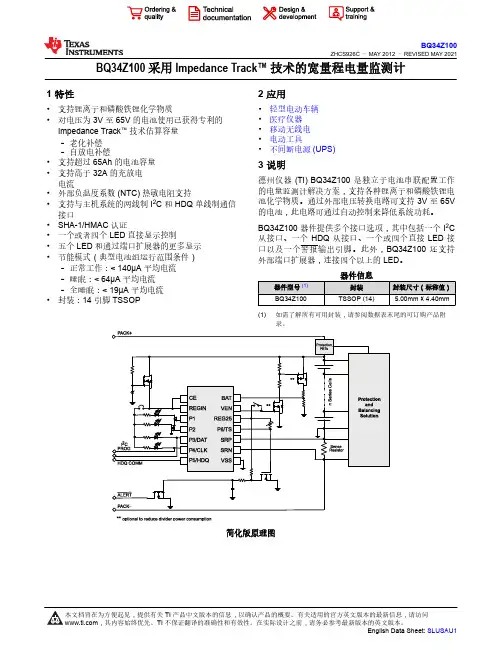
BQ34Z100 采用 Impedance Track™ 技术的宽量程电量监测计1 特性•支持锂离子和磷酸铁锂化学物质•对电压为 3V 至 65V 的电池使用已获得专利的 Impedance Track™技术估算容量–老化补偿–自放电补偿•支持超过 65Ah 的电池容量•支持高于 32A 的充放电电流•外部负温度系数 (NTC) 热敏电阻支持•支持与主机系统的两线制 I2C 和 HDQ 单线制通信接口•SHA-1/HMAC 认证•一个或者四个 LED 直接显示控制•五个 LED 和通过端口扩展器的更多显示•节能模式(典型电池组运行范围条件)–正常工作:< 140µA 平均电流–睡眠:< 64µA 平均电流–全睡眠:< 19µA 平均电流•封装:14 引脚 TSSOP 2 应用•轻型电动车辆•医疗仪器•移动无线电•电动工具•不间断电源 (UPS)3 说明德州仪器 (TI) BQ34Z100 是独立于电池串联配置工作的电量监测计解决方案,支持各种锂离子和磷酸铁锂电池化学物质。
通过外部电压转换电路可支持 3V 至 65V 的电池,此电路可通过自动控制来降低系统功耗。
BQ34Z100 器件提供多个接口选项,其中包括一个 I2C 从接口、一个 HDQ 从接口、一个或四个直接 LED 接口以及一个警报输出引脚。
此外,BQ34Z100 还支持外部端口扩展器,连接四个以上的 LED。
(1)如需了解所有可用封装,请参阅数据表末尾的可订购产品附录。
简化版原理图Table of Contents1 特性...................................................................................12 应用...................................................................................13 说明...................................................................................14 Revision History ..............................................................25 Pin Configuration and Functions ...................................36 Specifications ..................................................................46.1 Absolute Maximum Ratings........................................46.2 ESD Ratings...............................................................46.3 Recommended Operating Conditions.........................46.4 Thermal Information....................................................56.5 Electrical Characteristics: Power-On Reset................56.6 Electrical Characteristics: LDO Regulator...................56.7 Electrical Characteristics: Internal TemperatureSensor Characteristics..................................................56.8 Electrical Characteristics: Low-FrequencyOscillator.......................................................................66.9 Electrical Characteristics: High-FrequencyOscillator.......................................................................66.10 Electrical Characteristics: Integrating ADC(Coulomb Counter) Characteristics...............................66.11 Electrical Characteristics: ADC (Temperatureand Cell Measurement) Characteristics........................66.12 Electrical Characteristics: Data Flash MemoryCharacteristics (7)6.13 Timing Requirements: HDQ Communication............76.14 Timing Requirements: I 2C-Compatible Interface......86.15 Typical Characteristics..............................................97 Detailed Description ......................................................107.1 Overview...................................................................107.2 Feature Description...................................................117.3 Device Functional Modes..........................................398 Application and Implementation ..................................408.1 Typical Applications..................................................409 Power Supply Recommendations ................................4910 Layout ...........................................................................5010.1 Layout Guidelines...................................................5010.2 Layout Example......................................................5011 Device and Documentation Support ..........................5311.1 Documentation Support..........................................5311.2 接收文档更新通知...................................................5311.3 支持资源..................................................................5311.4 Trademarks.............................................................5311.5 Electrostatic Discharge Caution..............................5311.6 术语表.....................................................................5312 Mechanical, Packaging, and OrderableInformation (53)4 Revision History注:以前版本的页码可能与当前版本的页码不同Changes from Revision B (December 2012) to Revision C (May 2021)Page•根据更新的德州仪器 (TI) 标准更改了文档格式并通篇更新了 SRP 和 SRN 引脚................................................1•Changed Ground System ................................................................................................................................50•Changed Board Offset Considerations ............................................................................................................51Changes from Revision A (September 2012) to Revision B (December 2012)Page•Changed Absolute Maximum Ratings ...............................................................................................................4•Changed 节 6.3 ..................................................................................................................................................4•Changed 节 7.2.15.3 ........................................................................................................................................39•Changed SLEEP Mode ....................................................................................................................................39•Changed FULL SLEEP Mode ..........................................................................................................................39•Changed STEP 3 (44)BQ34Z100ZHCS926C – MAY 2012 – REVISED MAY 20215 Pin Configuration and FunctionsP2P3/SDA VEN P4/SCL P1P5/HDQ BAT P6/TS CE SRN REGIN SRP REG25VSSBQ34Z100ZHCS926C – MAY 2012 – REVISED MAY 2021BQ34Z100ZHCS926C – MAY 2012 – REVISED MAY 6 Specifications6.1 Absolute Maximum Ratings(1)(1)Stresses beyond those listed under absolute maximum ratings may cause permanent damage to the device. These are stress ratingsonly, and functional operation of the device at these or any other conditions beyond those indicated under recommended operating conditions is not implied. Exposure to absolute–maximum–rated conditions for extended periods may affect device reliability.6.2 ESD Ratings(1)JEDEC document JEP155 states that 500-V HBM allows safe manufacturing with a standard ESD control process.(2)JEDEC document JEP157 states that 250-V CDM allows safe manufacturing with a standard ESD control process.6.3 Recommended Operating Conditions6.3 Recommended Operating Conditions (continued)6.4 Thermal Information(1)For more information about traditional and new thermal metrics, see the Semiconductor and IC Package Thermal Metrics Application Report , SPRA953.6.5 Electrical Characteristics: Power-On Reset6.6 Electrical Characteristics: LDO Regulator(1)(1)LDO output current, I OUT , is the sum of internal and external load currents.(2)Specified by design. Not production tested.6.7 Electrical Characteristics: Internal Temperature Sensor CharacteristicsBQ34Z100ZHCS926C – MAY 2012 – REVISED MAY 2021BQ34Z100ZHCS926C – MAY 2012 – REVISED MAY 6.8 Electrical Characteristics: Low-Frequency Oscillator(1)The frequency drift is included and measured from the trimmed frequency at VCC = 2.5 V, T A = 25°C.(2)The frequency error is measured from 32.768 kHz.(3)The startup time is defined as the time it takes for the oscillator output frequency to be ±3%.6.9 Electrical Characteristics: High-Frequency Oscillator(1)The frequency error is measured from 2.097 MHz.(2)The startup time is defined as the time it takes for the oscillator output frequency to be ±3%.6.10 Electrical Characteristics: Integrating ADC (Coulomb Counter) Characteristics(1)Specified by design. Not tested in production.(2)Full-scale reference6.11 Electrical Characteristics: ADC (Temperature and Cell Measurement) Characteristics6.11 Electrical Characteristics: ADC (Temperature and Cell Measurement) Characteristics (continued)(1)Specified by design. Not tested in production.6.12 Electrical Characteristics: Data Flash Memory Characteristics(1)Specified by design. Not tested in production.6.13 Timing Requirements: HDQ CommunicationT A = –40°C to 85°C, C REG = 1.0 μF, 2.45 V < V REGIN = V BAT < 5.5 V; typical values at T A = 25°C and V REGIN = V BAT = 3.6 VBQ34Z100ZHCS926C – MAY 2012 – REVISED MAY 2021(a)Break and Break Recovery(c)Host Transmitted Bit(d)Gauge Transmitted Bit(b)HDQ line rise time图 6-1. Timing Diagrams6.14 Timing Requirements: I2C-Compatible InterfaceT A = –40°C to 85°C, C REG = 0.47 μF, 2.45 V < V REGIN = V BAT < 5.5 V; typical values at T A = 25°C and V REGIN = V BAT = 3.6t SU(STA)SCLSDAt w(H)tw(L)t f tr t(BUF)t rt d(STA)REPEATEDSTARTt h(DAT)t su(DAT)t f t su(STOP)STOP START图 6-2. I2C-Compatible Interface Timing DiagramsBQ34Z100ZHCS926C – MAY 2012 – REVISED MAY 6.15 Typical CharacteristicsBQ34Z100ZHCS926C – MAY 2012 – REVISED MAY 2021BQ34Z100ZHCS926C – MAY 2012 – REVISED MAY 7 Detailed Description7.1 OverviewThe BQ34Z100 device accurately predicts the battery capacity and other operational characteristics of a single cell or multiple rechargeable cell blocks, which are voltage balanced when resting. The device supports various Li-ion and LiFePO4 chemistries, and can be interrogated by a host processor to provide cell information, such as remaining capacity, full charge capacity, and average current.Information is accessed through a series of commands called Standard Data Commands (see 节7.2.1.1). Further capabilities are provided by the additional Extended Data Commands set (see 节 7.2.2). Both sets of commands, indicated by the general format Command(), are used to read and write information contained within the BQ34Z100 device’s control and status registers, as well as its data flash locations. Commands are sent from host to gauge using the BQ34Z100 serial communications engines, HDQ and I2C, and can be executed during application development, pack manufacture, or end-equipment operation.Cell information is stored in the BQ34Z100 in non-volatile flash memory. Many of these data flash locations are accessible during application development and pack manufacture. They cannot, generally, be accessed directly during end-equipment operation. Access to these locations is achieved by using the BQ34Z100 device’s companion evaluation software, through individual commands, or through a sequence of data-flash-access commands. To access a desired data flash location, the correct data flash subclass and offset must be known. The BQ34Z100 provides 32 bytes of user-programmable data flash memory. This data space is accessed through a data flash interface. For specifics on accessing the data flash, refer to 节 7.2.3.The key to the BQ34Z100 device’s high-accuracy gas gauging prediction is Texas Instrument’s proprietary Impedance Track algorithm. This algorithm uses voltage measurements, characteristics, and properties to create state-of-charge predictions that can achieve accuracy with as little as 1% error across a wide variety of operating conditions.The BQ34Z100 measures charge/discharge activity by monitoring the voltage across a small-value series sense resistor connected in the low side of the battery circuit. When an application’s load is applied, cell impedance is measured by comparing its Open Circuit Voltage (OCV) with its measured voltage under loading conditions.The BQ34Z100 can use an NTC thermistor (default is Semitec 103AT or Mitsubishi BN35-3H103FB-50) for temperature measurement, or can also be configured to use its internal temperature sensor. The BQ34Z100 uses temperature to monitor the battery-pack environment, which is used for fuel gauging and cell protection functionality.To minimize power consumption, the BQ34Z100 has three power modes: NORMAL, SLEEP, and FULL SLEEP. The BQ34Z100 passes automatically between these modes, depending upon the occurrence of specific events. Multiple modes are available for configuring from one to 16 LEDs as an indicator of remaining state of charge. More than four LEDs require the use of one or two inexpensive SN74HC164 shift register expanders.A SHA-1/HMAC-based battery pack authentication feature is also implemented on the BQ34Z100. When the IC is in UNSEALED mode, authentication keys can be (re)assigned. A scratch pad area is used to receive challenge information from a host and to export SHA-1/HMAC encrypted responses. See 节 7.2.14.1 for further details.备注Formatting conventions in this document:Commands: italics with parentheses and no breaking spaces; for example, RemainingCapacity().Data Flash: italics, bold, and breaking spaces; for example, Design Capacity.Register Bits and Flags: brackets only; for example, [TDA] DataFlash Bits: italic and bold; for example, [LED1]Modes and states: ALL CAPITALS; for example, UNSEALED mode.7.2 Feature Description7.2.1 Data Commands7.2.1.1 Standard Data CommandsThe BQ34Z100 uses a series of 2-byte standard commands to enable host reading and writing of battery information. Each standard command has an associated command-code pair, as indicated in 表 7-1. Because each command consists of two bytes of data, two consecutive HDQ/I2C transmissions must be executed to initiate the command function and to read or write the corresponding two bytes of data. Standard commands are accessible in NORMAL operation. Also, two block commands are available to read Manufacturer Name and Device Chemistry. Read/Write permissions depend on the active access mode.7.2.1.2 Control(): 0x00/0x01Issuing a Control() command requires a subsequent two-byte subcommand. These additional bytes specify the particular control function desired. The Control()command allows the host to control specific features of the BQ34Z100 during normal operation, and additional features when the BQ34Z100 is in different access modes, as described in 表 7-2.7.2.1.2.1 CONTROL_STATUS: 0x0000Instructs the fuel gauge to return status information to Control addresses 0x00/0x01. The status word includes the following information.Legend: RSVD = ReservedFAS:Status bit that indicates the BQ34Z100 is in FULL ACCESS SEALED state. Active when set.SS:Status bit that indicates the BQ34Z100 is in the SEALED state. Active when set.CALMODE:Status bit that indicates the BQ34Z100 calibration function is active. True when set.Default is 0.CCA:Status bit that indicates the BQ34Z100 Coulomb Counter Calibration routine is active. Active when set.BCA:Status bit that indicates the BQ34Z100 Board Calibration routine is active. Active when set.CSV:Status bit that indicates a valid data flash checksum has been generated. Active when set.FULLSLEEP:Status bit that indicates the BQ34Z100 is in FULL SLEEP mode. True when set. The state can only be detected by monitoring the power used by the BQ34Z100 because any communication will automatically clear it.SLEEP:Status bit that indicates the BQ34Z100 is in SLEEP mode. True when set.LDMD:Status bit that indicates the BQ34Z100 Impedance Track algorithm using constant-power mode. True when set.Default is 0 (CONSTANT CURRENT mode).RUP_DIS:Status bit that indicates the BQ34Z100 Ra table updates are disabled. True when set.VOK:Status bit that indicates cell voltages are OK for Qmax updates. True when set.QEN:Status bit that indicates the BQ34Z100 Qmax updates are enabled. True when set.7.2.1.2.2 DEVICE TYPE: 0x0001Instructs the fuel gauge to return the device type to addresses 0x00/0x01.7.2.1.2.3 FW_VERSION: 0x0002Instructs the fuel gauge to return the firmware version to addresses 0x00/0x01.7.2.1.2.4 HW_VERSION: 0x0003Instructs the fuel gauge to return the hardware version to addresses 0x00/0x01.7.2.1.2.5 RESET_DATA: 0x0005Instructs the fuel gauge to return the number of resets performed to addresses 0x00/0x01.7.2.1.2.6 PREV_MACWRITE: 0x0007Instructs the fuel gauge to return the previous command written to addresses 0x00/0x01. The value returned is limited to less than 0x0020.7.2.1.2.7 CHEM ID: 0x0008Instructs the fuel gauge to return the chemical identifier for the Impedance Track configuration to addresses 0x00/0x01.7.2.1.2.8 BOARD_OFFSET: 0x0009Instructs the fuel gauge to calibrate board offset. During board offset calibration the [BCA] bit is set.7.2.1.2.9 CC_OFFSET: 0x000AInstructs the fuel gauge to calibrate the coulomb counter offset. During calibration the [CCA] bit is set.7.2.1.2.10 CC_OFFSET_SAVE: 0x000BInstructs the fuel gauge to save the coulomb counter offset after calibration.7.2.1.2.11 DF_VERSION: 0x000CInstructs the fuel gauge to return the data flash version to addresses 0x00/0x01.7.2.1.2.12 SET_FULLSLEEP: 0x0010Instructs the fuel gauge to set the FULLSLEEP bit in the Control Status register to 1. This allows the gauge to enter the FULL SLEEP power mode after the transition to SLEEP power state is detected. In FULL SLEEP mode, less power is consumed by disabling an oscillator circuit used by the communication engines. For HDQ communication, one host message will be dropped. For I2C communications, the first I2C message will incur a 6-ms–8-ms clock stretch while the oscillator is started and stabilized. A communication to the device in FULL SLEEP will force the part back to the SLEEP mode.7.2.1.2.13 STATIC_CHEM_DF_CHKSUM: 0x0017Instructs the fuel gauge to calculate chemistry checksum as a 16-bit unsigned integer sum of all static chemistry data. The most significant bit (MSB) of the checksum is masked yielding a 15-bit checksum. This checksum is compared with the value stored in the data flash Static Chem DF Checksum. If the value matches, the MSB will be cleared to indicate a pass. If it does not match, the MSB will be set to indicate a failure.7.2.1.2.14 SEALED: 0x0020Instructs the fuel gauge to transition from UNSEALED state to SEALED state. The fuel gauge should always be set to SEALED state for use in customer’s end equipment.7.2.1.2.15 IT ENABLE: 0x0021Forces the fuel gauge to begin the Impedance Track algorithm, sets Bit 2 of UpdateStatus and causes the [VOK] and [QEN] flags to be set in the CONTROL STATUS register. [VOK] is cleared if the voltages are not suitable for a Qmax update. Once set, [QEN] cannot be cleared. This command is only available when the fuel gauge is UNSEALED and is typically enabled at the last step of production after the system test is completed.7.2.1.2.16 RESET: 0x0041Instructs the fuel gauge to perform a full reset. This command is only available when the fuel gauge is UNSEALED.7.2.1.2.17 EXIT_CAL: 0x0080Instructs the fuel gauge to exit CALIBRATION mode.7.2.1.2.18 ENTER_CAL: 0x0081Instructs the fuel gauge to enter CALIBRATION mode.7.2.1.2.19 OFFSET_CAL: 0x0082Instructs the fuel gauge to perform offset calibration.7.2.1.3 StateOfCharge(): 0x02/0x03This read-only function returns an unsigned integer value of the predicted remaining battery capacity expressed as a percentage of FullChargeCapacity() with a range of 0 to 100%.7.2.1.4 RemainingCapacity(): 0x04/0x05This read-only command pair returns the compensated battery capacity remaining. Unit is 1 mAh per bit.7.2.1.5 FullChargeCapacity(): 0x06/07This read-only command pair returns the compensated capacity of the battery when fully charged. Unit is 1 mAh per bit except if X10 mode is selected. In X10 mode, units are 10 mAh per bit. with units of 1 mAh per bit. . FullChargeCapacity() is updated at regular intervals, as specified by the Impedance Track algorithm.7.2.1.6 Voltage(): 0x08/0x09This read-word function returns an unsigned integer value of the measured cell-pack voltage in mV with a range of 0 V to 65535 mV.7.2.1.7 AverageCurrent(): 0x0A/0x0BThis read-only command pair returns a signed integer value that is the average current flowing through the sense resistor. It is updated every 1 second. Unit is 1 mA per bit except if X10 mode is selected. In X10 mode, units are 10 mA per bit. with units of 1 mA per bit.7.2.1.8 Temperature(): 0x0C/0x0DThis read-word function returns an unsigned integer value of the temperature, in units of 0.1 K, measured by the gas gauge and has a range of 0 to 6553.5 K. The source of the measured temperature is configured by the [TEMPS] bit in the Pack Configuration register (see 节 7.2.2).7.2.1.9 Flags(): 0x0E/0x0FThis read-word function returns the contents of the Gas Gauge Status register, depicting current operation status.Legend: RSVD = ReservedOTC:Overtemperature in Charge condition is detected. True when setOTD:Overtemperature in Discharge condition is detected. True when setBATHI:Battery High bit that indicates a high battery voltage condition. Refer to the data flash BATTERY HIGH parameters for threshold settings.BATLOW:Battery Low bit that indicates a low battery voltage condition. Refer to the data flash BATTERY LOW parameters for threshold settings.CHG_INH:Charge Inhibit: unable to begin charging. Refer to the data flash [Charge Inhibit Temp Low, Charge Inhibit Temp High] . True when setXCHG:Charging not allowedRSVD:ReservedFC:Full charge is detected. FC is set when charge termination is reached and FC Set% = –1 (see 节 7.2.10 for details) or StateOfCharge() is larger than FC Set% and FC Set% is not –1. True when setCHG:(Fast) charging allowed. True when setOCVTAKEN:Cleared on entry to RELAX mode and set to 1 when OCV measurement is performed in RELAX mode.ISD:Internal Short is detected. True when set. TDD = Tab Disconnect is detected. True when setSOC1:State-of-Charge Threshold 1 reached. True when setSOCF:State-of-Charge Threshold Final reached. True when setDSG:Discharging detected. True when set7.2.2 Extended Data CommandsExtended commands offer additional functionality beyond the standard set of commands. They are used in the same manner; however, unlike standard commands, extended commands are not limited to 2-byte words. The number of command bytes for a given extended command ranges in size from single to multiple bytes, as specified in 表 7-6. For details on the SEALED and UNSEALED states, refer to 节 7.2.3.3.(1)SEALED and UNSEALED states are entered via commands to CNTL 0x00/0x01.(2)In SEALED mode, data flash cannot be accessed through commands 0x3E and 0x3F.7.2.2.1 AtRate(): 0X10/0x11The AtRate() read-/write-word function is the first half of a two-function call-set used to set the AtRate value used in calculations made by the AtRateTimeToEmpty() function. The AtRate() units are in mA.The AtRate() value is a signed integer and both positive and negative values will be interpreted as a discharge current value. The AtRateTimeToEmpty()function returns the predicted operating time at the AtRate value of discharge. The default value for AtRate() is zero and will force AtRate() to return 65535.7.2.2.2 AtRateTimeToEmpty(): 0x12/0x13This read-word function returns an unsigned integer value of the predicted remaining operating time if the battery is discharged at the AtRate() value in minutes with a range of 0 to 65534. A value of 65535 indicatesAtRate() = 0.The gas gauge updates AtRateTimeToEmpty() within 1s after the host sets the AtRate() value. The gas gauge automatically updates AtRateTimeToEmpty() based on the AtRate() value every 1 s.7.2.2.3 Current(): 0x10/0x11This read-only command pair returns a signed integer value that is the current flow through the sense resistor. It is updated every 1 second. Units are 1 mA per bit except if X10 mode is selected. In X10 mode, units are 10 mA per bit.with units of 1mA. However, if PackConfiguration [SCALED]is set then the units have been scaled through the calibration process. The actual scale is not set in the device and SCALED is just an indicator flag.7.2.2.4 NominalAvailableCapacity(): 0x14/0x15This read-only command pair returns the uncompensated (no or light load) battery capacity remaining. Unit is 1 mAh per bit.7.2.2.5 FullAvailableCapacity(): 0x16/0x17This read-only command pair returns the uncompensated (no or light load) capacity of the battery when fully charged. Unit is 1 mAh per bit. FullAvailableCapacity()is updated at regular intervals, as specified by the Impedance Track algorithm.7.2.2.6 TimeToEmpty(): 0x18/0x19This read-only function returns an unsigned integer value of the predicted remaining battery life at the present rate of discharge , in minutes. A value of 65535 indicates that the battery is not being discharged.This read-only function returns an unsigned integer value of predicted remaining time until the battery reaches full charge, in minutes, based upon AverageCurrent(). The computation should account for the taper current time extension from the linear TTF computation based on a fixed AverageCurrent() rate of charge accumulation. A value of 65535 indicates the battery is not being charged.7.2.2.8 StandbyCurrent(): 0x1C/0x1DThis read-only function returns a signed integer value of the measured standby current through the sense resistor. The StandbyCurrent() is an adaptive measurement. Initially, it reports the standby current programmed in Initial Standby, and after spending some time in standby, reports the measured standby current.The register value is updated every 1 second when the measured current is above the Deadband (3 mA default) and is less than or equal to 2 x Initial Standby. The first and last values that meet this criterion should not be averaged in, since they may not be stable values. To approximate a 1 minute time constant, each new StandbyCurrent() value is computed as follows:StandbyCurrent()NEW = (239/256) × StandbyCurrent()OLD + (17/256) × AverageCurrent()7.2.2.9 StandbyTimeToEmpty(): 0x1E/0x1FThis read-only function returns an unsigned integer value of the predicted remaining battery life at the standby rate of discharge, in minutes. The computation should use Nominal Available Capacity (NAC), the uncompensated remaining capacity, for this computation. A value of 65535 indicates battery is not being discharged.7.2.2.10 MaxLoadCurrent(): 0x20/0x21This read-only function returns a signed integer value, in units of mA, of the maximum load conditions. The MaxLoadCurrent()is an adaptive measurement which is initially it reports the maximum load current programmed in Initial Max Load Current. If the measured current is ever greater than Initial Max Load Current, then MaxLoadCurrent() updates to the new current. MaxLoadCurrent() is reduced to the average of the previous value and Initial Max Load Current whenever the battery is charged to full after a previous discharge to an SOC less than 50%. This prevents the reported value from maintaining an unusually high value.7.2.2.11 MaxLoadTimeToEmpty(): 0x22/0x23This read-only function returns an unsigned integer value of the predicted remaining battery life at the maximum load current discharge rate, in minutes. A value of 65535 indicates that the battery is not being discharged.7.2.2.12 AvailableEnergy(): 0x24/0x25This read-only function returns an unsigned integer value of the predicted charge or energy remaining in the battery. The value is reported in units of mWh.7.2.2.13 AveragePower(): 0x26/0x27This read-word function returns an unsigned integer value of the average power of the current discharge. A value of 0 indicates that the battery is not being discharged. The value is reported in units of mW.7.2.2.14 TimeToEmptyAtConstantPower(): 0x28/0x29This read-only function returns an unsigned integer value of the predicted remaining operating time if the battery is discharged at the AveragePower() value in minutes. A value of 65535 indicates AveragePower() = 0. The gas gauge automatically updates TimeToEmptyatContantPower() based on the AveragePower() value every 1s.7.2.2.15 InternalTemp(): 0x2A/0x2BThis read-only function returns an unsigned integer value of the measured internal temperature of the device, in units of 0.1 K, measured by the fuel gauge.。

TI(德州仪器)德州仪器,简称TI,全球约 30,300人,总部位于美国得克萨斯州的达拉斯,2008年营业额为185亿美元, 是全球领先的半导体公司,为现实世界的信号处理提供创新的数字信号处理(DSP)及模拟技术, 应用领域涵盖无线通讯、宽带、网络家电、数字马达控制与消费类市场。
TI(德州仪器)目录更多关于产品•MSP430系列单片机•TMS370系列单片机•TMS470系列单片机•Stellaris系列单片机•32位C2000单片机•C2000 DSP•C5000 DSP•C6000 DSP•达芬奇 DSP•A/D转换器•D/A转换器•电池管理•PWM控制器•DC/DC控制器MSP430系列单片机MSP430 系列是一个 16 位的、具有精简指令集的、超低功耗的混合型单片机,在 1996 年问世,由于它具有极低的功耗、丰富的片内外设和方便灵活的开发手段,已成为众多单片机系列中一颗耀眼的新星。
MSP430 系列单片机的迅速发展和应用范围的不断扩大,主要取决于以下的特点。
强大的处理能力 MSP430 系列单片机是一个 16 位的单片机,采用了精简指令集( RISC )结构,具有丰富的寻址方式( 7 种源操作数寻址、 4 种目的操作数寻址)、简洁的 27 条内核指令以及大量的模拟指令;大量的寄存器以及片内数据存储器都可参加多种运算;还有高效的查表处理指令;有较高的处理速度,在 8MHz 晶体驱动下指令周期为 125 ns 。
这些特点保证了可编制出高效率的源程序。
在运算速度方面, MSP430 系列单片机能在 8MHz 晶体的驱动下,实现 125ns 的指令周期。
16 位的数据宽度、 125ns 的指令周期以及多功能的硬件乘法器(能实现乘加)相配合,能实现数字信号处理的某些算法(如 FFT 等)。
MSP430 系列单片机的中断源较多,并且可以任意嵌套,使用时灵活方便。
当系统处于省电的备用状态时,用中断请求将它唤醒只用 6us 。
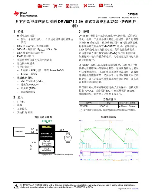
Copyright © 2017, Texas Instruments IncorporatedProduct Folder Order Now Technical Documents Tools &SoftwareSupport &CommunityDRV8871ZHCSE26B –AUGUST 2015–REVISED JULY 2016具有内部电流感测功能的DRV88713.6A 刷式直流电机驱动器(PWM 控制)1特性•H 桥电机驱动器–驱动一个直流电机、一个步进电机的绕组或其他负载• 6.5V 至45V 宽工作电压范围•565m Ω(典型值)R DS(on)(HS +LS)• 3.6A 峰值电流驱动能力•PWM 控制接口•无需感测电阻即可实现电流调节•低功耗休眠模式•小型封装尺寸–8引脚HSOP 封装,带有PowerPAD™– 4.9mm ×6mm •集成保护特性–VM 欠压闭锁(UVLO)–过流保护(OCP)–热关断(TSD)–自动故障恢复2应用•打印机•电器•工业设备•其他机电应用3说明DRV8871器件是一款刷式直流电机驱动器,适用于打印机、电器、工业设备以及其他小型机器。
两个逻辑输入控制H 桥驱动器,该驱动器由四个N 沟道金属氧化物半导体场效应晶体管(MOSFET)组成,能够以高达3.6A 的峰值电流双向控制电机。
利用电流衰减模式,可通过对输入进行脉宽调制(PWM)来控制电机转速。
如果将两个输入均置为低电平,则电机驱动器将进入低功耗休眠模式。
DRV8871器件具有高级电流调节电路,该电路不使用模拟电压基准或外部感应电阻器。
这种新型解决方案采用标准的低成本、低功耗电阻来设置电流阈值。
该器件能够将电流限制在某一已知水平,这可显著降低系统功耗要求,并且无需大容量电容来维持稳定电压,尤其是在电机启动和停转时。
该器件针对故障和短路问题提供了全面保护,包括欠压锁定(UVLO)、过流保护(OCP)和过热保护(TSD)。
德州仪器芯片命名规则德州仪器(Texas Instruments,简称TI)是全球领先的半导体设计和制造公司之一,其产品涵盖了广泛的应用领域,包括计算机、通信、汽车、工业控制、医疗设备等。
作为半导体行业的重要组成部分,芯片命名规则对于产品的识别和区分起着关键的作用。
下面将介绍德州仪器芯片的命名规则。
在德州仪器的芯片命名规则中,主要分为两个部分:前缀和功能标识。
1.前缀:前缀是芯片型号的第一个字母或几个字母,用于标识该芯片的主要类型。
以下是一些常见的前缀及其含义:-T:指示该芯片属于德州仪器公司产品。
-C:指示该芯片属于德州仪器的应用专用芯片产品。
-SN:指示该芯片属于德州仪器的运算放大器产品。
-LM:指示该芯片属于德州仪器的线性产品,如运算放大器、电压比较器等。
-OPA:指示该芯片属于德州仪器的运算放大器产品。
-TLC:指示该芯片属于德州仪器的逻辑电平转换产品。
-DRV:指示该芯片属于德州仪器的驱动器产品。
-MSP:指示该芯片属于德州仪器的微控制器系列产品。
2.功能标识:-功能标识是芯片型号的剩余部分,用于标识芯片的功能特性、系列等。
德州仪器的功能标识通常由字母和数字组成。
- 第一个字母通常表示芯片系列,如数字信号处理器(DSP)、运算放大器(Op-Amp)等。
-后面的数字则表示具体的功能特性和版本等。
不同数字对应不同的产品特性,比如频率范围、精度等。
除了前缀和功能标识外,德州仪器的芯片命名规则还可能包括尺寸、封装和温度范围等信息。
这些附加信息可以进一步细化芯片的具体规格和应用环境,有助于用户选择适合自己需求的芯片产品。
需要注意的是,芯片型号命名规则在不同的产品系列和产品类型中可能存在一定的差异,以上只是对德州仪器一般的命名规则进行了介绍。
对于具体的产品型号,用户还需要参考德州仪器的官方文档和资料进行查询和确认。
总结起来,德州仪器芯片的命名规则包括前缀和功能标识两个部分。
前缀标识了产品的主要类型,而功能标识则用于表示芯片的具体功能特性和版本等。
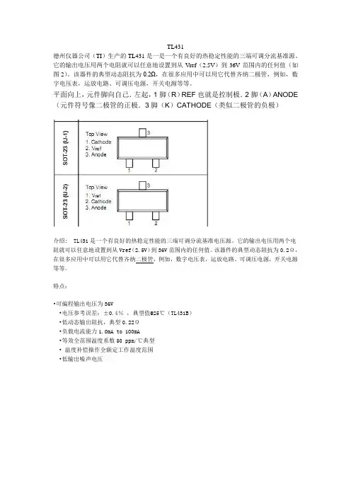
TL431德州仪器公司(TI)生产的TL431是一是一个有良好的热稳定性能的三端可调分流基准源。
它的输出电压用两个电阻就可以任意地设置到从Vref(2.5V)到36V范围内的任何值(如图2)。
该器件的典型动态阻抗为0.2Ω,在很多应用中可以用它代替齐纳二极管,例如,数字电压表,运放电路、可调压电源,开关电源等等。
平面向上,元件脚向自己.左起,1脚(R)REF也就是控制极.2脚(A)ANODE (元件符号像二极管的正极.3脚(K)CATHODE(类似二极管的负极)介绍: TL431是一个有良好的热稳定性能的三端可调分流基准电压源。
它的输出电压用两个电阻就可以任意地设置到从Vref(2.5V)到36V范围内的任何值。
该器件的典型动态阻抗为0.2Ω,在很多应用中可以用它代替齐纳二极管,例如,数字电压表,运放电路、可调压电源,开关电源等等。
特点:•可编程输出电压为36V•电压参考误差:±0.4%,典型值@25℃(TL431B)•低动态输出阻抗,典型0.22Ω•负载电流能力1.0mA to 100mA•等效全范围温度系数50 ppm/℃典型• 温度补偿操作全额定工作温度范围•低输出噪声电压图1 TO92封装引脚图图2 8脚封装引脚功能图3 SOP-8 贴片封装引脚图图4 TL431符号及内部方框图图5 TL431内部电路图MAXIMUM RATINGS (Full operating ambient temperature range applies, unless otherwise noted.)最大额定值(环境温度范围适用,除非另有说明。
)RECOMMENDED OPERATING CONDITIONS建议操作条件ELECTRICAL CHARACTERISTICS(TA=25℃, unless otherwise noted.)电气特性(25℃ ,除非另有说明。
)ELECTRICAL CHARACTERISTICS (TA = 25℃, unless otherwise noted.)电气特性(25℃,除非另有说明。
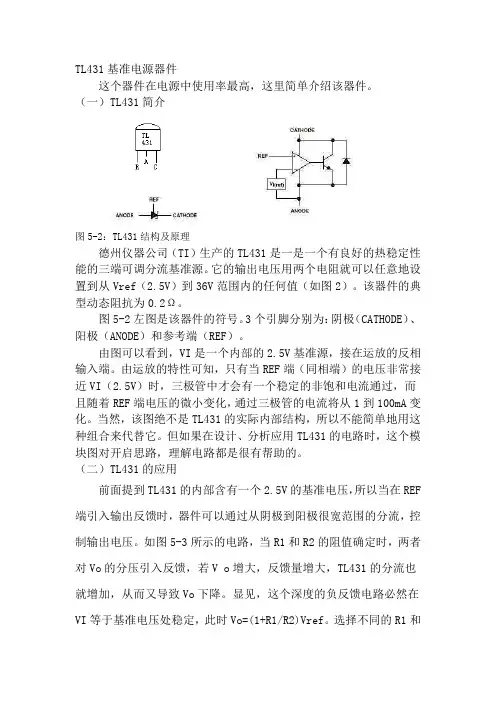
TL431基准电源器件这个器件在电源中使用率最高,这里简单介绍该器件。
(一)TL431简介图5-2:TL431结构及原理德州仪器公司(TI)生产的TL431是一是一个有良好的热稳定性能的三端可调分流基准源。
它的输出电压用两个电阻就可以任意地设置到从Vref(2.5V)到36V范围内的任何值(如图2)。
该器件的典型动态阻抗为0.2Ω。
图5-2左图是该器件的符号。
3个引脚分别为:阴极(CATHODE)、阳极(ANODE)和参考端(REF)。
由图可以看到,VI是一个内部的2.5V基准源,接在运放的反相输入端。
由运放的特性可知,只有当REF端(同相端)的电压非常接近VI(2.5V)时,三极管中才会有一个稳定的非饱和电流通过,而且随着REF端电压的微小变化,通过三极管的电流将从1到100mA变化。
当然,该图绝不是TL431的实际内部结构,所以不能简单地用这种组合来代替它。
但如果在设计、分析应用TL431的电路时,这个模块图对开启思路,理解电路都是很有帮助的。
(二)TL431的应用前面提到TL431的内部含有一个2.5V的基准电压,所以当在REF 端引入输出反馈时,器件可以通过从阴极到阳极很宽范围的分流,控制输出电压。
如图5-3所示的电路,当R1和R2的阻值确定时,两者对Vo的分压引入反馈,若V o增大,反馈量增大,TL431的分流也就增加,从而又导致Vo下降。
显见,这个深度的负反馈电路必然在VI等于基准电压处稳定,此时Vo=(1+R1/R2)Vref。
选择不同的R1和R2的值可以得到从2.5V到36V范围内的任意电压输出,特别地,当R1=R2时,Vo=5V。
需要注意的是,在选择电阻时必须保证TL431工作的必要条件,就是通过阴极的电流要大于1 mA 。
当然,这个电路并不太实用,但它很清晰地展示了该器件在应用中的方法。
将这个电路稍加改动,就可以得到在很多实用的电源电路,如图5-4。
一般地,在阴极和参考端之间,可以引进R、C串联网络,以做相位补偿。
DMD工作原理介绍DMD,即数字微型反射镜器件(Digital Micro-mirror Device),是一种利用微型反射镜阵列实现图像显示和光学投射的技术。
DMD是由德州仪器(Texas Instruments)公司发明并推广的,是一种基于微机械系统(MEMS)的光学设备。
在DMD中,数百万个微小的反射镜根据输入信号的控制模式进行快速调节,从而实现对光的反射和制备出复杂的图像。
DMD的基本组成是一个正方形的芯片,芯片上布满了微小的单晶硅反射镜。
每个反射镜的大小约为10-15微米,而整个芯片上有数百万个反射镜。
每个反射镜的底部通过支撑结构与芯片连接,而顶部则可以根据控制电信号的输入而自由旋转。
当反射镜转到角度为±12°左右时,反射镜上的光线会被反向反射。
DMD的工作原理可以分为三个阶段来解释:扫描切换、光成像和图像显示。
在扫描切换阶段,DMD芯片上的所有反射镜都按照固定的顺序进行扫描。
每个反射镜都有一个驱动电路来控制其偏转。
对于每个扫描周期,芯片上的每个反射镜会从初始位置向两个方向之一旋转,形成一个1-bit图像,即只有两个可能的状态:+12°或-12°。
DMD的扫描速度非常快,可以达到每秒几千次,使得人眼无法察觉到这种切换。
在光成像阶段,通过使用镜头和光源来照射在DMD芯片上的反射镜上。
每个反射镜的旋转状态将决定光线是被反向反射还是向正前方传播。
通过控制每个反射镜上光线的反射方式,可以通过调整光路实现对光的强弱调节,进而形成不同灰度的图像。
在图像显示阶段,DMD芯片的驱动电路通过一个控制板将要显示的图像数据传输给芯片上的反射镜。
反射镜根据这些输入信号进行调节,选择性地反射光线以形成对应的图像。
通过快速的扫描切换和光线反射调节,DMD就可以实现高帧率和高分辨率的图像显示。
相比其他显示技术,DMD具有如下几个优点:1.高亮度和对比度:由于DMD采用反射式显示方式,较少的能量损失会使得图像更加亮度和清晰。
cd4093工作原理CD4093是一种CMOS集成电路,具有四个独立的双稳态触发器。
它是由德州仪器公司(Texas Instruments)推出的,常用于数字逻辑电路和计时电路中。
本文将对CD4093的工作原理进行详细的介绍。
一、CD4093的基本结构CD4093由四个独立的双稳态触发器(flip-flop)组成,每个双稳态触发器由两个与非门(NAND gate)和一个反馈路径构成。
整个芯片有14个引脚,其中包括输入引脚、输出引脚、电源引脚和接地引脚。
二、双稳态触发器的基本原理双稳态触发器是一种存储器件,可以存储一个二进制状态(0或1)。
它具有两个互补的输出引脚(Q和Q'),根据输入信号的状态,可以切换输出引脚的状态。
在CD4093中,每个双稳态触发器由两个与非门和一个反馈路径构成。
与非门是基本的逻辑门,具有两个输入和一个输出。
当两个输入都为1时,输出为0;否则输出为1。
反馈路径可以将输出信号重新引入到与非门的输入端。
双稳态触发器的工作原理是利用了与非门的互补输出特性和反馈路径的正反馈特性。
当输入信号改变时,与非门的输出也会改变。
这个改变会通过反馈路径重新引入到与非门的输入端,从而使输出保持在新的状态。
另外,在引脚上,由于非门的特殊结构,一个引脚既可以作为输入也可以作为输出。
三、CD4093的工作原理每个双稳态触发器都具有两个输入引脚(A和B)和两个输出引脚(Q和Q')。
输入信号通过A和B引脚输入,输出信号通过Q和Q'引脚输出。
无论是A还是B输入引脚只要有一个引脚为高电平(1),那么与非门的输出就会为低电平(0),这时的输出信号将通过反馈路径回到与非门的输入引脚中,使得输出引脚保持在低电平。
只有当A和B引脚都为低电平时,与非门的输出为高电平(1),这时的输出信号不会经过反馈路径,输出引脚会保持在高电平状态。
四、CD4093的使用方法CD4093广泛应用于数字逻辑电路和计时电路中。
德州仪器简介德州仪器简介德州仪器(Texas Instruments),简称TI,是全球领先的半导体公司,为现实世界的信号处理提供创新的数字信号处理(DSP)及模拟器件技术。
除半导体业务外,还提供包括教育产品和数字光源处理解决方案(DLP)。
德州仪器总部位于美国得克萨斯州的达拉斯,并在25多个国家设有制造、设计或销售机构。
研发经费:2005年为20.2亿美元; 2006年预计为22亿美元资本支出:2005年为13.3亿美元; 2006年预计为13亿美元在2006年财富(Fortune)500大企业排名为167 (根据2005财政年度)员工人数:全球约有30,300人各地分布如下:美国:15,900人亚洲:8,800人日本:2,400人欧洲:3,200人[编辑]德州仪器全球各地主要的设计及制造场所分布[编辑]德州仪器亚洲区德州仪器自1950年代起在亚洲地区开始运营,首先从事销售和市场工作,以及应用技术支持,然后迅速增加半导体装配与测试设施等业务。
亚洲现在是德州仪器最先进和重要的半导体硅片制造工厂的基地之一。
除此之外,德州仪器亚洲市场还涵盖教育产品,包括教学计算器。
亚洲区设厂地点及时间中国(1986)菲律宾(1979)马来西亚(1972)新加坡(1968)澳洲(1958) 印度(1985)韩国(1977)台湾(1969)香港(1967)[编辑]德州仪器在中国德州仪器自1986年进入中国大陆以来,一直高度关注中国市场的发展。
经过公司董事会批准的德州仪器中国发展战略于1996年正式实施。
此战略的目标是帮助中国建立合理的电子产品结构,并且提高高科技产品的设计能力,力求以全球领先的DSP技术支持中国高科技产业走向世界。
为贯彻此战略,德州仪器除在中国建立了庞大的半导体代理商销售网外,还在北京、上海、深圳及香港设立了办事处及技术支持队伍,提供许多独特的产品及服务,包括DSP和模拟器件产品、硬件和软件开发工具以及设计咨询服务等。
德州仪器(TI) 宣布推出具有无与伦比连接选项与定点和浮点功能的全新处理器——OMAP-L138,同时这四款产品也是业界功耗最低的浮点数字信号处理器(DSP),可充分满足高能效、连通性设计对高集成度外设、更低热量耗散以及更长电池使用寿命的需求。
上述器件结合了一系列独特的应用优化特性和外设,能显著降低工业、通信、医疗诊断和音频等多种产品的总体系统成本。
例如,继电保护系统可充分受益于OMAP-L138 器件的定点/浮点DSP、ARM9、以太网控制器(EMAC) 与LCD 控制器,其成本较当前解决方案可降低近14 美元。
对诸如测量测试、公共安全无线电、音乐特效以及智能家居传感器等需要高速数据传输和高容量存储的应用而言,这些处理器不仅具备通用并行端口(uPP),同时也是TI 首批集成串行高级技术附件(SATA)的器件。
这些产品拥有高达300 MHz 的性能,可通过动态电压与频率缩放(DVFS) 及多种省电模式管理片上电源。
若配合TI 电源管理软件和配套模拟解决方案,开发人员无需成为节能技术专家即可优化系统,提高性能,降低功耗。
为了简化设计工作,缩短开发时间,新产品都是引脚对引脚兼容,可与所有TMS320C6000 器件实现代码兼容,并配套提供低成本的实验板和功能齐备的评估板(EVM)。
OMAP-L138 处理器的特性与优势:·构建于C6748 DSP 基础之上的双内核处理器采用300 MHz ARM9,可为开发人员提供了高度的灵活性,从而使他们能够为其应用添加直观易用的人机接口、触摸屏或网络功能;·ARM9 使开发人员能够实施Linux 等高级操作系统;·预计将于2009 年第四季度提供Windows Embedded CE 及Integrity 支持;·不同使用情况下总功耗为440mW,待机模式功耗为15mW。
可满足各种专业技术水平要求的开发工具:·Logic 面向设计人员及制造商提供的社群支持实验板售价仅为149 美元,其采用OMAP-L138 模块上系统(SOM)、64 MB mDDR、开源Linux、DSP/BIOS 驱动程序,可用于上述四款产品任何一款的开发工作;·TI OMAP-L138/C6748 EVM 适用于需要全面外设接入、全方位TI技术支持的开发人员。
德州仪器(TI)产品命名规则产品分类及描述:该公司半导体产品分类较多,包括:存储器产品组、数字信号处理器(DSP)、电源管理IC、放大器和线性器件、微控制器、数据转换器、温度传感器和控制IC、标准线性器件等。
就我们日常所接到的询价情况来看,我将先主要介绍数字信号处理器(DSP)、微控制器、电源管理IC这三种。
♦数字信号处理器(DSP):DSP (digital singnal processor)芯片,也称数字信号处理器,是一种具有特殊结构的微处理器。
DSP芯片的内部采用程序和数据分开的哈佛结构,具有专门的硬件乘法器,广泛采用流水线操作,提供特殊的DSP指令,可以用来快速地实现各种数字信号处理算法。
根据数字信号处理的要求,DSP芯片一般具有如下的一些主要特点:(1)在一个指令周期内可完成一次乘法和一次加法。
(2)程序和数据空间分开,可以同时访问指令和数据。
(3)片内具有快速RAM,通常可通过独立的数据总线在两块中同时访问。
(4)具有低开销或无开销循环及跳转的硬件支持。
(5)快速的中断处理和硬件I/O支持。
(6)具有在单周期内操作的多个硬件地址产生器。
(7)可以并行执行多个操作。
(8)支持流水线操作,使取指、译码和执行等操作可以重叠执行。
与通用微处理器相比,DSP芯片的其他通用功能相对较弱些。
3、TI品牌电子芯片命名规则:SN54LS X X X /HC/HCT/或SNJ54LS/HC/HCT 中的后缀说明:SN或SNJ表示TI品牌SN军标,带N表示DIP封装,带J表示DIP (双列直插),带D表示表贴,带W表示宽体SNJ军级,后面代尾缀F或/883表示已检验过的军级.CD54LS X X X/HC/HCT:♦无后缀表示普军级♦后缀带J或883表75军品级CD4000/CD45X X:后缀带BCP或BE屈军品后缀带BF属普军级后缀带BF3A或883屈军品级TLX X X :后缀CP普通级IP工业级后缀带D是表贴后缀带MJB, MJG或带/883的为军品级TLC表示普通电压TLV低功耗电压TMS320系列归属DSP器件,MSP430F微处理器BB产品命名规则:前缀ADS模拟器件后缀U表贴P是DIP封装带B 表示工业级前缀INA, XTR, PGA等表示高精度运放后缀U表贴P 代表DIP PA表示高精度TI产品命名规则:SN54LS XXX /HC/HCT/或SNJ54LS/HC/HCT中的后缀说明:1、S N或S町表示TI品牌2、S N军标,带N表示DIP封装,带J表示DIP (双列直插),带D表示表贴,带W表示宽体3、S NJ军级,后面代尾缀F或/883表示已检验过的军级。
德州仪器(TI)产品命名规则产品分类及描述:该公司半导体产品分类较多,包括:存储器产品组、数字信号处理器(DSP)、电源管理IC、放大器和线性器件、微控制器、数据转换器、温度传感器和控制IC、标准线性器件等。
就我们日常所接到的询价情况来看,我将先主要介绍数字信号处理器(DSP)、微控制器、电源管理IC这三种。
◆数字信号处理器(DSP):DSP(digital singnal processor) 芯片,也称数字信号处理器,是一种具有特殊结构的微处理器。
DSP芯片的内部采用程序和数据分开的哈佛结构,具有专门的硬件乘法器,广泛采用流水线操作,提供特殊的DSP 指令,可以用来快速地实现各种数字信号处理算法。
根据数字信号处理的要求,DSP芯片一般具有如下的一些主要特点:(1)在一个指令周期内可完成一次乘法和一次加法。
(2)程序和数据空间分开,可以同时访问指令和数据。
(3)片内具有快速RAM,通常可通过独立的数据总线在两块中同时访问。
(4)具有低开销或无开销循环及跳转的硬件支持。
(5)快速的中断处理和硬件I/O支持。
(6)具有在单周期内操作的多个硬件地址产生器。
(7)可以并行执行多个操作。
(8)支持流水线操作,使取指、译码和执行等操作可以重叠执行。
与通用微处理器相比,DSP芯片的其他通用功能相对较弱些。
3、TI品牌电子芯片命名规则:SN54LS×××/HC/HCT/或SNJ54LS/HC/HCT中的后缀说明:SN或SNJ表示TI品牌SN军标,带N表示DIP封装,带J表示DIP(双列直插),带D表示表贴,带W表示宽体SNJ军级,后面代尾缀F或/883表示已检验过的军级.CD54LS×××/HC/HCT:◆无后缀表示普军级◆后缀带J或883表示军品级CD4000/CD45××:后缀带BCP或BE属军品后缀带BF属普军级后缀带BF3A或883属军品级TL×××:后缀CP普通级 IP工业级后缀带D是表贴后缀带MJB,MJG或带/883的为军品级TLC表示普通电压 TLV低功耗电压TMS320系列归属DSP器件, MSP430F微处理器BB产品命名规则:前缀ADS模拟器件后缀U表贴 P是DIP封装带B表示工业级前缀INA,XTR,PGA等表示高精度运放后缀U表贴 P代表DIP PA表示高精度TI产品命名规则:SN54LS×××/HC/HCT/或SNJ54LS/HC/HCT中的后缀说明:1、SN或SNJ表示TI品牌2、SN军标,带N表示DIP封装,带J表示DIP(双列直插),带D表示表贴,带W表示宽体3、SNJ军级,后面代尾缀F或/883表示已检验过的军级。
TL431德州仪器公司(TI)生产的TL431是一是一个有良好的热稳定性能的三端可调分流基准源。
它的输出电压用两个电阻就可以任意地设置到从Vref(2.5V)到36V范围内的任何值(如图2)。
该器件的典型动态阻抗为0.2Ω,在很多应用中可以用它代替齐纳二极管,例如,数字电压表,运放电路、可调压电源,开关电源等等。
平面向上,元件脚向自己.左起,1脚(R)REF也就是控制极.2脚(A)ANODE(元件符号像二极管的正极.3脚(K)CATHODE (类似二极管的负极)介绍: TL431是一个有良好的热稳定性能的三端可调分流基准电压源。
它的输出电压用两个电阻就可以任意地设置到从Vref(2.5V)到36V范围内的任何值。
该器件的典型动态阻抗为0.2Ω,在很多应用中可以用它代替齐纳二极管,例如,数字电压表,运放电路、可调压电源,开关电源等等。
特点:•可编程输出电压为36V•电压参考误差:±0.4%,典型值@25℃(TL431B)•低动态输出阻抗,典型0.22Ω•负载电流能力1.0mA to 100mA•等效全范围温度系数50 ppm/℃典型•温度补偿操作全额定工作温度范围•低输出噪声电压图1 TO92封装引脚图图2 8脚封装引脚功能图3 SOP-8 贴片封装引脚图图4 TL431符号及内部方框图图5 TL431内部电路图MAXIMUM RATINGS (Full operating ambient temperature range applies, unlessotherwise noted.)最大额定值(环境温度范围适用,除非另有说明。
)RECOMMENDED OPERATING CONDITIONS建议操作条件ELECTRICAL CHARACTERISTICS(TA=25℃, unless otherwise noted.)电气特性(25℃,除非另有说明。
)ELECTRICAL CHARACTERISTICS (TA = 25℃, unless otherwise noted.)电气特性(25℃,除非另有说明。
74hc0474HC04是一种常用的六通道反相器芯片,属于高速CMOS器件系列。
它由TI(德州仪器)公司推出,具有广泛的应用领域和可靠的性能。
本文将介绍74HC04的功能、特点、引脚配置以及一些常见的应用。
一、功能和特点74HC04是一种六通道反相器,每个通道都可以独立地工作,输入为高电平时输出为低电平,输入为低电平时输出为高电平。
其工作电压范围为2V至6V,具有非常低的功耗,适合用于低功率应用。
同时,74HC04具有高速的传输速度,使其适用于高速数字电路和大规模数字集成电路。
74HC04采用CMOS技术,具有抗干扰能力强、噪声低等特点,可以在恶劣的环境条件下稳定工作。
此外,它还具有广泛的工作温度范围,可在-40℃至85℃的温度下正常工作。
二、引脚配置74HC04的引脚配置如下图所示:┌───┐1A ─── 1│ │14 ─── VCC1Y ─── 2│ │13 ─── 2A2A ─── 3│ │12 ─── 2Y2Y ─── 4│ │11 ─── 3A3A ─── 5│ │10 ─── 3Y3Y ─── 6│ │9 ─── GND│ │8 ─── 4A│ │7 ─── 4Y└───┘在上图中,VCC为电源正极,GND为电源负极。
1A、2A和3A为输入引脚,1Y、2Y和3Y为输出引脚,4A和4Y为未使用引脚。
三、应用示例1. 信号转换74HC04可用于信号转换的应用。
例如,当需要将一个高电平信号转换为低电平信号时,可以将高电平信号连接到输入引脚(如1A),输出引脚(如1Y)即可输出对应的低电平信号。
2. 时钟缓冲在数字系统中,时钟信号(CLK)常常需要经过缓冲处理,以提供更稳定和准确的时钟信号。
74HC04可以作为时钟缓冲器来使用,将输入引脚连接到时钟源,将输出引脚连接到需要使用时钟信号的模块。
3. 逻辑电路设计74HC04可以用于逻辑电路设计,例如构建简单的逻辑门电路。
通过适当连接输入和输出引脚,可以实现与门、或门、非门等逻辑功能。
7416芯片7416芯片是德州仪器(Texas Instruments)公司生产的数字电子集成电路。
它是一款具有4个双输入与非门(NAND门)功能的集成电路芯片。
下面将介绍该芯片的主要特点、功能和应用领域。
7416芯片的主要特点如下:1. 集成度高:该芯片内部包含4个双输入与非门电路,能够实现多个与非门电路的功能需求。
2. 高速操作:7416芯片具有快速的响应速度和高达250MHz的工作频率,能够满足高速电路的需求。
3. 低功耗:该芯片采用低功耗设计,能够在工作时保持较低的功耗,从而减少能源消耗。
4. 外接器件简单:7416芯片只需要外接输入信号和电源电压,不需要额外的电阻、电容等外接元件,使用非常简单方便。
7416芯片的主要功能如下:1. 与非门功能:该芯片内部包含4个双输入与非门,每个与非门有两个输入端(A、B)和一个输出端(Y)。
当输入端A和输入端B同时为逻辑0时,输出端Y为逻辑1;否则,输出端Y为逻辑0。
2. 逻辑运算功能:由于与非门是一种基本的逻辑门,7416芯片可以用于实现各种复杂的逻辑运算,如与门、或门、异或门等。
3. 时序控制功能:该芯片可以用于实现时序控制,通过与非门的组合,可以产生各种时序信号,实现电路的时序控制。
7416芯片的应用领域如下:1. 通信设备:由于7416芯片具有高速操作和低功耗的特点,适用于通信设备中的高速信号处理和时序控制电路。
2. 数字电子产品:该芯片可应用于数字电子产品中的各种逻辑运算和时序控制电路,如电视机、数码相机等。
3. 工控设备:7416芯片在工控设备中可以用于实现各种逻辑控制和时序控制功能,如自动化生产设备和机器人控制等。
总结起来,7416芯片是一款具有4个双输入与非门功能的集成电路芯片,具有高集成度、高速操作和低功耗等特点,广泛应用于通信设备、数字电子产品和工控设备等领域。
DMD介绍DMD芯⽚显⽰原理的介绍DMD精微反射镜⾯是⼀种整合的微机电上层结构电路单元 (MEMS superstructure cell),它是利⽤CMOS SRAM记忆晶胞所制成。
DMD上层结构的制造是从完整CMOS内存电路开始,再透过光罩层的使⽤,制造出铝⾦属层和硬化光阻层(hardened photoresist) 交替的上层结构,铝⾦属层包括地址电极 (address electrode)、绞链(hinge)、轭 (yoke) 和反射镜,硬化光阻层则作为牺牲层 (sacrificial layer),⽤来形成两个空⽓间 (air gaps)。
铝⾦属会经过溅镀沉积 (sputter-deposited)以及电浆蚀刻 (plasma-etched)处理,牺牲层则会经过电浆去灰 (plasma-ashed) 处理,以便制造出层间的空⽓间隙每个微反射镜都能将光线从两个⽅向反射出去,实际反射⽅向则视底层记忆晶胞的状态⽽定;当记忆晶胞处于「ON」状态时,反射镜会旋转⾄+12度,记忆晶胞处于「OFF」状态,反射镜会旋转⾄-12度。
只要结合DMD以及适当光源和投影光学系统,反射镜就会把⼊射光反射进⼊或是离开投影镜头的透光孔,使得「ON」状态的反射镜看起来⾮常明亮,「OFF」状态的反射镜看起来就很⿊暗。
利⽤⼆位脉冲宽度调变可以得到灰阶效果,如果使⽤固定式或旋转式彩⾊滤镜,再搭配⼀颗或三颗DMD芯⽚,即可得到彩⾊显⽰效果。
DMD的输⼊是由电流代表的电⼦字符,输出则是光学字符,这种光调变或开关技术⼜称为⼆位脉冲宽度调变 (binary pulsewidth modulation),它会把8位字符送⾄DMD的每个数字光开关输⼊端,产⽣28或256个灰阶。
最简单的地址序列 (address sequence) 是将可供使⽤的字符时间 (field time) 分成⼋个部份,再从最⾼有效位(MSB) 到最低有效位(LSB),依序在每个位时间使⽤⼀个地址序列。