SV503中文规格书
- 格式:pdf
- 大小:509.59 KB
- 文档页数:4

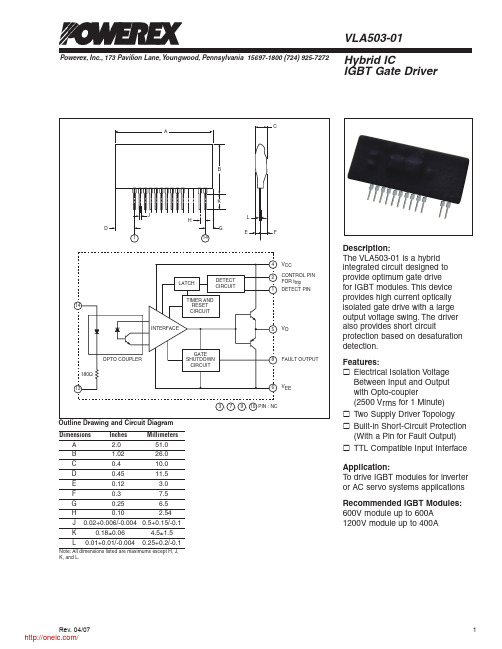
Powerex, Inc., 173 Pavilion Lane, Youngwood, Pennsylvania 15697-1800 (724) 925-7272Hybrid ICIGBT Gate DriverVLA503-01Rev. 04/07Description:The VLA503-01 is a hybrid integrated circuit designed to provide optimum gate drive for IGBT modules. This device provides high current optically isolated gate drive with a large output voltage swing. The driver also provides short circuitprotection based on desaturation detection.Features:£ Electrical Isolation Voltage Between Input and Output with Opto-coupler(2500 V rms for 1 Minute)£ Two Supply Driver Topology £ Built-in Short-Circuit Protection (With a Pin for Fault Output)£ TTL Compatible Input Interface Application:To drive IGBT modules for inverter or AC servo systems applications Recommended IGBT Modules:600V module up to 600A 1200V module up to 400ADimensions Inches Millimeters A 2.0 51.0 B 1.02 26.0 C 0.4 10.0 D 0.45 11.5 E 0.12 3.0 F 0.3 7.5 G 0.25 6.5 H 0.10 2.54 J 0.02+0.006/-0.004 0.5+0.15/-0.1 K 0.18±0.06 4.5±1.5 L 0.01+0.01/-0.004 0.25+0.2/-0.1Note: All dimensions listed are maximums except H, J, K, and L./Powerex, Inc., 173 Pavilion Lane, Youngwood, Pennsylvania 15697-1800 (724) 925-7272VLA503-01Hybrid IC IGBT Gate DriverAbsolute Maximum Ratings, T a = 25°C unless otherwise specifiedCharacteristics Symbol VLA503-01 Units Supply Voltage, DC V CC 18 VoltsV EE-15 Volts Input Signal Voltage (Applied between Pin 13 - 14, 50% Duty Cycle, Pulse Width 1ms) V i -1 ~ +7 Volts Output Voltage (When the Output Voltage is "H") V O V CC Volts Output Current I OHP-5 Amperes (Pulse Width 2µs, f ≤ 20kHz) I OLP 5 Amperes Isolation Voltage (Sine Wave Voltage 60Hz, for 1 Minute) V ISO2500 V rms Case Temperature T C85 °C Operating Temperature (No Condensation Allowable) T opr-20 ~ +60 °C Storage Temperature (No Condensation Allowable) T stg-25 ~ +100* °C Fault Output Current (Applied Pin 8) I FO 20 mA Input Voltage at Pin 1 (Applied Pin 1) V R1 50 Volts *Differs from H/C condition.Electrical and Mechanical Characteristics, T a = 25°C unless otherwise specified, V CC = 15V, V EE = -10V) Characteristics Symbol Test Conditions Min. Typ. Max. Units Supply Voltage V CC Recommended Range 14 15 — VoltsV EE Recommended Range -7 — -10 Volts Pull-up Voltage on Primary Side V IN Recommended Range 4.75 5 5.25 Volts "H" Input Current I IH Recommended Range 15.2 16 19 mA Switching Frequency f Recommended Range — — 20 kHz Gate Resistance R G Recommended Range 2 — — W "H" Input Current I IH V IN = 5V — 16 — mA "H" Output Voltage V OH13 14 — Volts "L" Output Voltage V OL-8 -9 — Volts "L-H" Propagation Time t PLH I IH = 16mA — 0.5 1 µs "L-H" Rise Time t r I IH = 16mA — 0.3 1 µs "H-L" Propagation Time t PHL I IH = 16mA — 1 1.3 µs "H-L" Fall Time t f I IH = 16mA — 0.3 1 µs Timer t timer Between Start and Cancel 1 — 2 ms(Under Input Sign "L")Fault Output Current I FO Applied 8 Pin, R = 4.7k W— 5 — mA Controlled Time Detect Short-Circuit 1 t trip1Pin 1: 15V and More, Pin 2: Open — 2.6 — µs Controlled Time Detect Short-Circuit 2** t trip2Pin 1: 15V and More, Pins 2-4: 10pF — 3 — µs(Connective Capacitance)SC Detect Voltage V SC Collector Voltage of Module 15 — — Volts **Length of wiring capacitor controlled time detect short-circuit is within 5cm from Pin 2 and Pin 4 coming and going.Rev. 04/07 /VLA503-01Hybrid IC IGBT Gate DriverPowerex, Inc., 173 Pavilion Lane, Youngwood, Pennsylvania 15697-1800 (724) 925-7272Rev. 04/07FAULTFAULTApplication Circuit/VLA503-01Hybrid IC IGBT Gate DriverPowerex, Inc., 173 Pavilion Lane, Youngwood, Pennsylvania 15697-1800 (724) 925-72724Rev. 04/07020604080AMBIENT TEMPERATURE, T a , (°C)010302040SUPPL Y VOLTAGE, V CC , (VOLTS)(PIN: 4 – 6)1.01.61.41.20.80.60.20.4P R O P A G A T I O N D E L A Y T I M E “L -H ”, t P L H , (µs )P R O P A G A T I O N D E L A Y T I M E “H -L ”, t P H L , (µs )0956784320257510012550150CONNECTIVE CAPACITANCE, C trip , (p F )(PIN: 2 – 4)C O N T R O L L ED T I ME S H O R T -C I R C U I T D E T E C T , t t r i p , (µs )01PROPAGATION DELAY TIME VS. AMBIENT CHARACTERISTICS(TYPICAL)PROPAGATION DELAY TIME VS. INPUT VOLTAGE CHARACTERISTICS(TYPICAL)PROPAGATION DELAY TIME VS.AMBIENT TEMPERATURE CHARACTERISTICS(TYPICAL)SWITCHING TIME DEFINITIONSV IN(PIN 14 TO 13)V O(PIN 5 TO 6)/VLA503-01Hybrid IC IGBT Gate DriverPowerex, Inc., 173 Pavilion Lane, Youngwood, Pennsylvania 15697-1800 (724) 925-7272Rev. 04/07General DescriptionThe VLA503-01 is a hybrid integrated circuit designed to provide gate drive for high power IGBT modules. This circuit has been optimized for use with Powerex NF-Series and A-Series IGBT modules. However, the output characteristics are compatible with most MOS gated power devices. The VLA503-01 features a compact single-in-line package design. The upright mounting minimizes required printed circuit board space to allow efficient and flexible layout. The VLA503-01 converts logic level control signals into fully isolated +15V/-8V gate drive with up to 5A of peak drive current. Control signal isolation is provided by an integrated high speed opto-coupler. Short circuit protection is provided by means of destauration detection. Short Circuit ProtectionFigure 1 shows a block diagram of a typical desatura-tion detector. In this circuit, a high voltage fast recovery diode (D1) is connected to the IGBT’s collector to moni-tor the collector to emitter voltage. When the IGBT is in the off state, V CE is high and D1 is reverse biased. With D1 off the (+) input of the comparator is pulled up to the positive gate drive power supply (V+) which is normally +15V . When the IGBT turns on, the compara-tors (+) input is pulled down by D1 to the IGBT’s V CE(sat). The (-) input of the comparator is supplied with a fixed voltage (V TRIP ). During a normal on-state condition the comparator’s (+) input will be less than V TRIP and it’s output will be low. During a normal off-state condi-tion the comparator’s (+) input will be larger than V TRIPand it’s output will be high. If the IGBT turns on into a short circuit, the high current will cause the IGBT’s col-lector-emitter voltage to rise above V TRIP even though the gate of the IGBT is being driven on. This abnormal presence of high V CE when the IGBT is supposed to be on is often called desaturation . Desaturation can be detected by a logical AND of the driver’s input signal and the comparator output. When the output of the AND goes high a short circuit is indicated. The output of the AND can be used to command the IGBT to shut down in order to protect it from the short circuit. A delay (t TRIP ) must be provided after the comparator output to allow for the normal turn on time of the IGBT. The t TRIP delay is set so that the IGBTs V CE has enough time to fall below V TRIP during normal turn on switching. If t TRIP is set too short, erroneous desaturation detection will occur. The maximum allowable t TRIP delay is limited by the IGBT’s short circuit withstanding capability. In typical applications using Powerex IGBT modules the recom-mended limit is 10µs.Operation of the VLA503-01 Desaturation Detector The Powerex VLA503-01 incorporates short circuit protection using desaturation detection as described above. A flow chart for the logical operation of the short-circuit protection is shown in Figure 2. When a desaturation is detected the hybrid gate driver performs a soft shut down of the IGBT and starts a timed (t timer ) 1.5ms lock out. The soft turn-off helps to limit the tran-sient voltage that may be generated while interrupting the large short circuit current flowing in the IGBT . During the lock out the driver pulls Pin 8 low to indicate the fault status. Normal operation of the driver will resume after the lock-out time has expired and the control input signal returns to its off state.Adjustment of Trip TimeThe VLA503-01 has a default short-circuit detection time delay (t TRIP ) of approximately 2.5µs. This will prevent erroneous detection of short-circuit conditions as long as the series gate resistance (R G ) is near the minimum recommended value for the module being used. The 2.5µs delay is appropriate for most applica-tions so adjustment will not be necessary. However, in some low frequency applications it may be desirable to use a larger series gate resistor to slow the switching of the IGBT, reduce noise, and limit turn-off transient volt-ages. When R G is increased, the switching delay time of the IGBT will also increase. If the delay becomesINPUTFigure 1. Desaturation Detector/VLA503-01Hybrid IC IGBT Gate DriverPowerex, Inc., 173 Pavilion Lane, Youngwood, Pennsylvania 15697-1800 (724) 925-7272 Rev. 04/07Figure 2. VLA503-01 Desaturation DetectorV Figure 3. Adjustment of t triplong enough so that the voltage on the detect Pin 1 is greater than V SC at the end of the t TRIP delay the driver will erroneously indicate that a short circuit has occurred. T o avoid this condition the VLA503-01 has provisions for extending the t TRIP delay by connecting a capacitor (C TRIP ) between Pin 2 and V CC (Pins 4). The effect of adding C TRIP on trip time is shown in Figure 3. If t TRIP is extended care must be exercised not to exceed the short-circuit withstanding capability of the IGBT mod-ule. Normally this will be satisfied for Powerex NF and A-Series IGBT modules as long as the total shut-down time does not exceed 10µs./分销商库存信息: POWEREXVLA503-01。

T racer™ Controller MP503 Input/OutputCopyright© 2012 Trane. All rights reserved.This document and the information in it are the property of Trane and may not be usedor reproduced in whole or in part, without the written permission of Trane. Trane reservesthe right to revise this publication at any time and to make changes to its content withoutobligation to notify any person of such revision or change.T rademarksTrane and its logo are trademarks of Trane in the United States and other countries. Alltrademarks referenced in this document are the trademarks of their respective owners.Revision SummaryBAS-PRC009-EN (30 May 2012)Cost Savings: Update to mount plate and metal enclosure to remove metal screw/nut and useplastic PEM nut. Change to figure illustrations.T able of ContentsProduct Overview . . . . . . . . . . . . . . . . . . . . . . . . . . . . . . . . . . . . . . . . . . . . . . . . . . . . . . 4 Universal Inputs . . . . . . . . . . . . . . . . . . . . . . . . . . . . . . . . . . . . . . . . . . . . . . . . . . . 4Binary outputs . . . . . . . . . . . . . . . . . . . . . . . . . . . . . . . . . . . . . . . . . . . . . . . . . . . . . 4 Features . . . . . . . . . . . . . . . . . . . . . . . . . . . . . . . . . . . . . . . . . . . . . . . . . . . . . . . . . . . . . . . 5Wiring Diagram . . . . . . . . . . . . . . . . . . . . . . . . . . . . . . . . . . . . . . . . . . . . . . . . . . . . . . . . 7Network Architecture . . . . . . . . . . . . . . . . . . . . . . . . . . . . . . . . . . . . . . . . . . . . . . . . . . . 8Dimensions and Specifications . . . . . . . . . . . . . . . . . . . . . . . . . . . . . . . . . . . . . . . . . . 9 Dimensions . . . . . . . . . . . . . . . . . . . . . . . . . . . . . . . . . . . . . . . . . . . . . . . . . . . . . . . 9Power . . . . . . . . . . . . . . . . . . . . . . . . . . . . . . . . . . . . . . . . . . . . . . . . . . . . . . . . . . . 10Operating Environment . . . . . . . . . . . . . . . . . . . . . . . . . . . . . . . . . . . . . . . . . . . . 10Storage Environment . . . . . . . . . . . . . . . . . . . . . . . . . . . . . . . . . . . . . . . . . . . . . . 10Analog-to-Digital Conversion . . . . . . . . . . . . . . . . . . . . . . . . . . . . . . . . . . . . . . . 10Power Supply for Inputs . . . . . . . . . . . . . . . . . . . . . . . . . . . . . . . . . . . . . . . . . . . 10Outputs . . . . . . . . . . . . . . . . . . . . . . . . . . . . . . . . . . . . . . . . . . . . . . . . . . . . . . . . . . 10Agency Listings/Compliance . . . . . . . . . . . . . . . . . . . . . . . . . . . . . . . . . . . . . . . 10Product OverviewThe Tracer MP503 input/output (I/O) module is a configurable, multi-purpose device used toprovide data monitoring and binary control as part of a building automation system (BAS).Communication between the module and a BAS occurs over a LonTalk communication link.The Tracer MP503 I/O module is in a compact enclosure. It can monitor a wide variety of sensedconditions and provide equipment start/stop, or other switched states, based on communicatedcommands from a peer device or higher level BAS.The Tracer MP503 I/O module includes four universal inputs and four binary outputs. Universal InputsEach of the four universal inputs can be configured for use with any of the following:•Trane 10 kW thermistor temperature sensor•0–20 mA or 0–10 Vdc sensor•Binary (dry-contact) deviceBinary outputsEach of the four binary outputs can be controlled independently, as commanded from a peercontrol device or higher level BASFeaturesApplication FlexibilityTracer MP503 I/O modules may be located anywhere in a building, wherever up to four monitoringand/or four binary control points are needed. By connecting the Tracer MP503 to a LonTalk network,input data can be sent from and commands can be sent to the Tracer MP503.The Tracer MP503 I/O module can be used in a wide variety of monitoring and control applications.Typical applications include monitoring of the following:•Room, duct, or water temperatures•Relative humidity in rooms or ductwork•Pressure sensing, including duct static pressure and hydronic differential pressures•Status of fan or pump operationThe outputs can be used for on/off functions including:•Fan control•Pump control•Lighting control•Staging of heating or cooling equipment.Easy InstallationThe Tracer MP503 is suitable for indoor mounting in a variety of locations. Screw terminals that areclearly labeled ensure that wires are connected quickly and accurately. A compact enclosure designsimplifies installation in small spacesConfigurable InputsEach of the four universal inputs can be easily configured using the Trane Tracker (BMTK) light-commercial system controller or the Rover service software tool. Each input is individuallyselectable for input signal type, and the value of the input signal is then transmitted to any otherpeer device on the LonTalk network or BAS.Internal 24 Vdc Sensor Power SupplyThe Tracer MP503 has a built-in 80 mA, 24 Vdc power supply capable of powering 4–20 mAtransmitting sensors. This capability eliminates the need for auxiliary power supplies. Any of thefour inputs can be used with 4–20 mA sensors.12-bit Analog-to-Digital (A/D) ConversionThe four universal inputs of the Tracer MP503 provide very precise sensing of measured variablesthrough the use of high-resolution analog-to-digital converters.Output Status LEDsLight-emitting diodes (LEDs) located on the Tracer MP503 board indicate the status of each of thefour binary outputs. An LED lights up whenever its respective binary output is energized. With aglance at these visual indicators, you can tell if the associated controlled device is on or off.Output Default OptionsEach of the four binary outputs has a default state provided to ensure fail-safe operation ofcontrolled equipment in the event of a system-level communications loss. The output can beconfigured to default to off or on, or can maintain its current state.Wide Ambient Operating T emperaturesThe Tracer MP503 has an extended operating temperature range from –40°F to 158°F (from –40°Cto 70°C). Because of this extended range, the module can be placed in locations not suitable forFeaturesother building control modules. If the module is used outdoors, it should be placed in a suitableNEMA-4 enclosure (not included), for weather protection.InteroperabilityThe Tracer MP503 I/O module communicates using the LonTalk FTT-10A communication protocol.The Trane implementation of this protocol is also referred to as Comm5. Comm5 allows thecontrollers to operate in peer-to-peer configuration and to communicate with other compatiblebuilding control systems. The module supports LonMark standard network variable types (SNVTs),allowing the module to be used with the Trane Tracer Summit and Tracker (BMTK) building controlsystems, as well as other building control systems that support the LonTalk protocol.Wiring DiagramTypical relay on/off0–10 Vdc sensorNetwork ArchitectureThe Tracer MP503 can operate on a Tracer Summit building automation system (shown below), aTracker (BMTK) system, or as part of a peer-to-peer network.The Tracer MP503 can be configured using the Rover service tool for Tracer controllers or other PC-based service tools compliant with the EIA/CEA-860 standard. This tool can be connected at anyaccessible location on the LonTalk Comm5 communication link.•Carbon dioxide (CO2)Dimensions and SpecificationsDimensionsPlastic Cover Model Dimensions•Height: 5.375 in. (137 mm) Width: 6.875 in. (175 mm) Depth: 2.0 in. (51 mm)Metal Enclosure Model DimensionsHeight: 9.0 in. (25 mm) Width: 10.37 in. (263 mm) Depth: 2.25 in. (58 mm)5.625 in.(143 mm)6.3 in (160 mm)5.375 in.(137 mm)2.0 in.(51 mm)6.875 in.(175 mm)6.875 in.(175 mm)Dimensions and SpecificationsPower•Supply: 20–30 Vac (24 Vac nominal) at 50/60 Hz•Consumption: 10 VA plus 12VA (maximum) per binary output Operating Environment•Temperature: From -40 to 158°F (-40 to 70°C)•Relative humidity: From 5 to 95% non-condensing Storage Environment•Temperature: From –40 to 185°F (–40 to 85°C)•Relative humidity: From 5% to 95% non-condensing Analog-to-Digital Conversion•12-bit resolutionPower Supply for Inputs•24Vdc,80mAOutputs•24 Vac powered relays (12 VA maximum)Agency Listings/ComplianceCE Immunity:EN 50082-1:1997CE Emissions:EN 50081-1:1992 (CISPR 22)EN 61000-3-2, EN 610003-3UL/C-UL listed:Energy management systemUL 94-5V (UL flammability rating for plenum use)FCC Part 15, Class ADimensions and Specifications BAS-PRC009-EN 12 Jun 201211Trane optimizes the performance of homes and buildings around the world. A business of Ingersoll Rand, the leader in creating and sustaining safe, comfortable and energy efficient environments, Trane offers a broad portfolio of advanced controls and HVAC systems, comprehensive building services, and parts. For more information, visit .Trane has a policy of continuous product and product data improvement and reserves the right to change design and specifications without notice.We are committed to using environmentally conscious print practices that reduce waste.© 2012 Trane. All rights reserved.BAS-PRC009-EN 12 Jun 2012Supersedes BAS-PRC009-EN (23 Aug 2010)。

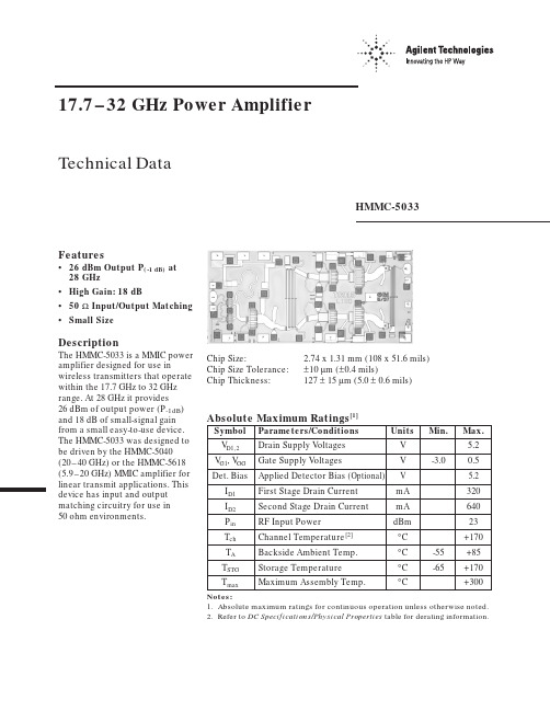
17.7–32 GHz Power Amplifier Technical DataFeatures•26 dBm Output P(-1dB) at28GHz•High Gain: 18dB•50Ω Input/Output Matching•Small SizeDescriptionThe HMMC-5033 is a MMIC poweramplifier designed for use inwireless transmitters that operatewithin the 17.7GHz to 32GHzrange. At 28GHz it provides26dBm of output power (P-1dB) and 18dB of small-signal gain from a small easy-to-use device. The HMMC-5033 was designed to be driven by the HMMC-5040 (20–40GHz) or the HMMC-5618 (5.9–20GHz) MMIC amplifier for linear transmit applications. This device has input and output matching circuitry for use in50ohm environments.Absolute Maximum Ratings[1]Symbol Parameters/Conditions Units Min.Max.V D1,2Drain Supply Voltages V 5.2V G1, VGGGate Supply Voltages V-3.00.5 Det. Bias Applied Detector Bias (Optional)V 5.2I D1First Stage Drain Current mA320I D2Second Stage Drain Current mA640P in RF Input Power dBm23T ch Channel Temperature[2]°C+170 T A Backside Ambient Temp.°C-55+85 T STG Storage Temperature°C-65+170 T max Maximum Assembly Temp.°C+300 Notes:1.Absolute maximum ratings for continuous operation unless otherwise noted.2.Refer to DC Specifications/Physical Properties table for derating information. Chip Size: 2.74 x 1.31 mm (108 x 51.6 mils)Chip Size Tolerance:±10 µm (±0.4 mils)Chip Thickness:127 ± 15 µm (5.0 ± 0.6 mils)HMMC-5033HMMC-5033 DC Specifications/Physical Properties[1]Symbol Parameters and Test Conditions Units Min.Typ.Max.V D1Drain Supply Operating Voltage V 3.55 V D2Drain Supply Operating Voltage V55I D1First Stage Drain Supply Current mA240320(V D1 = 3.5 V, V G1 = Open, V GG set for I D2 typical )I D2Second Stage Drain Supply Current mA460640(V D2 = 5 V, V GG = -0.8 V)V G1, V GG Gate Supply Operating Voltages V-0.8(I D1 + I D2≅ 700 mA)V P Pinch-off Voltage V-2.5-1.2-0.8 [V DD = 2.5 V, (I D1 + I D2) ≤ 20 mA]Det. Bias Detector Bias Voltage (Optional)V V D25θ1(ch-ba)First Stage Thermal Resistance[2]°C/Watt67 (Channel-to-Backside at T ch = 160°C)θ2(ch-bs)Second Stage Thermal Resistance[2]°C/Watt37 (Channel-to-Backside at T ch = 160°C)T ch Second Stage Channel Temperature[3] (T A = 75°C,°C160 MTTF ≥ 106 hrs, V D2 = 5 V, I D2 = 460 mA)Notes:1.Backside ambient operating temperature T A = 25°C unless otherwise noted.2.Thermal resistance (°C/Watt) at a channel temperature T (°C) can be estimated using the equation:θ(T) ≅θch-bs x [T(°C)+273] / [160°C+273].3.Derate MTTF by a factor of two for every 8°C above T ch.HMMC-5033 RF Specifications,T A = 25°C, Z O = 50 Ω, V D1 = 3.5 V, , V D2 = 5 V, I D2 = 460 mA, I D1 = 240 mALower Band Mid Band Upper BandSymbol Parameters/Conditions UnitsSpecifications Specifications Specifications Min.Typ.Max.Min.Typ.Max.Min.Typ.Max.BW Operating Bandwidth GHz17.7212126.52531.5 Gain Small Signal Gain dB172217201518P-1dB Output Power dBm222324252526 at 1 dB Gain CompressionP SAT Saturated Output Power[1]dBm252728(RL in)MIN Min. Input Return Loss dB8109121012(RL out)MIN Min. Output Return Loss dB152015201520 Isolation Min. Reverse Isolation dB505050Note:1. Devices operating continuously beyond 1 dB gain compression may experience power degradation.HMMC-5033 ApplicationsThe HMMC-5033 MMIC is a broadband power amplifier designed for use in transmitters that operate in various frequency bands between 17.7GHz and 32GHz. It can be attached to the output of the HMMC-5040(20–40GHz) or the HMMC-5618(5.9–20GHz) MMIC amplifier,increasing the power handling capability of transmitters requir-ing linear operation.Biasing and OperationThe recommended DC biascondition for optimum efficiency,performance, and reliability is V D1=3.5 volts and V D2=5 volts with V GG set for I D1+I D2= 700mA (no connection to V G1). This bias arrangement results in default drain currents I D1=240mA and I D2= 460 mA.A single DC gate supply con-nected to V GG will bias all gain stages.If operation with both V D1 and V D2 at 5 volts is desired, anadditional wire bond connectionfrom the V G1 pad to the V GG external bypass chip-capacitor (shorting V G1 to V GG ) will balance the currents in each gain stage.V GG (= V G1) can be adjusted for I D1+I D2= 700mA.Muting can be accomplished by setting V G1 and/or V GG to the pinch-off voltage V P .An optional output power detec-tor network is also provided.Detector sensitivity can be adjusted by biasing the diodes with typically 1 to 5 volts applied to the Det-Bias terminal. Simply connecting Det-Bias to the V D2supply is a convenient method of biasing this detector network.The differential voltage between the Det-Ref and Det-Out bonding pads can be correlated with the RF power emerging from the RF Output port.The RF ports are AC-coupled at the RF input to the first stage and the RF output of the second stage. If the output detector is biased using the on-chip optional Det-Bias network, an externalFigure 1. HMMC-5033 Simplified Schematic Diagram.AC-blocking capacitor may be required at the RF Output port.No ground wires are needed since ground connections are made with plated through-holes to the backside of the device.Assembly TechniquesElectrical and thermal conductive epoxy die attach is the preferred assembly method. Solder die attach using a fluxless gold-tin (AuSn) solder preform can also be used. The device should be attached to an electrically con-ductive surface to complete the DC and RF ground paths. The backside metallization on the device is gold.It is recommended that the electrical connections to the bonding pads be made using 0.7–1.0 mil diameter gold wire.The microwave/millimeter-wave connections should be kept as short as possible to minimize inductance. For assemblies requiring long bond wires,multiple wires can be attached to the RF bonding pads.Thermosonic wedge is the preferred method for wirebonding to the gold bond pads. A guided-wedge at an ultrasonic power level of 64 dB can be used for the 0.7 mil wire. The recom-mended wire bond stage tempera-ture is 150 ± 2°C.For more detailed information see Agilent application note #999,“GaAs MMIC Assembly and Handling Guidelines.”GaAs MMICs are ESD sensitive.Proper precautions should be used when handling these devices.V D2Det. OutV D1V G2 = V GGDet. Bias (Optional)Det. ReferenceV G1 (Optional)RF InputRF OutputHMMC-5033 Typical PerformanceFigure 2. Gain and Isolation vs. Frequency.S M A L L -S I G N A L G A I N (d B )FREQUENCY (GHz)V = 3.5 V, V = 5 V, I = 240 mA, I = 460 mAFigure 3. Input and Output Return Loss vs. Frequency.FREQUENCY (GHz)V = 3.5 V, V = 5 V, I = 240 mA, I= 460 mA V = 3.5 V, V = 5 V, I = 240 mA, I = 460 mAFigure 4. Output Power vs. Total Drain Current.P -1dB (d B m )I DD (mA)Figure 5. Output Power Loss vs. Frequency.P s a t (d B m )P -1d B (d B m )18202224262830323436FREQUENCY (GHz)V = 3.5 V, V = 5 V, I = 240 mA, I = 460 mAFigure 7. Detector Voltages vs. Output Power for Various Detector Bias Voltages.(R F D E T ) – (D C D E T ) (m V )1617182019212223252426RF OUTPUT POWER (dBm)V = 3.5 V, V = 5 V, I = 240 mA, I = 460 mAFigure 8. Gain and Total Drain Current vs. Output Power.G A I N (d B )I D D (m A )RF OUTPUT POWER (dBm)Figure 6. Gain Compression and Efficiency at 28 GHz.G A I N (d B )RF OUTPUT POWER (dBm)10121416281820222426301012141628182022242630Figure 9. Assembly diagram illustrating the HMMC-5033 cascaded with the HMMC-5040 for 20–32GHz applications.Figure 10. Assembly diagram illustrating the HMMC-5033 cascaded with the HMMC-5618 for 17.7–20GHz applications.RF OutputV G ≥100 pF 400 mARF OutputRF InputHMMC-5618400 mAThis data sheet contains a variety of typical and guaranteed performance data. The information supplied should not be interpreted as a complete list of circuit specifica-tions. In this data sheet the term typical refers to the 50th percentile performance.For additional information contact your local Agilent sales representative.Figure 11. HMMC-5033 Bonding Pad Locations. (Dimensions are in micrometers)1260116595635RF InputRF Output Det. Bias Det. Ref.Det. Out1180VG1V GGV D2V D28019702575269014574519802610 Data subject to change.Copyright © 1999 Agilent Technologies 5966-4573E (11/99)。

版权声明版权所有版权所有© 2001-2011 互普信息技术有限公司。
保留所有权利。
本手册之所有咨询皆有版权。
本手册之任何资料非经互普信息技术有限公司书面同意,不得以电子、机械、磁性、光学、化学、手写或任何之形式加以复制、传送、改写及存储在存取系统,或者翻译成任何语言或电脑语言。
请注意互普信息技术有限公司对本手册内容不做任何担保。
互普信息技术有限公司对于其中所含的错误,或遵照本手册资讯操作所引起必然或偶然之错误所造成的损害不负赔偿责任。
对于本手册的内容,互普信息技术有限公司拥有最终的解释权。
12第一章简介目录第一章.简介 (12)1.1前言 (12)1.2功能介绍 (13)第二章.安装和部署 (16)2.1基本运行框架 (16)2.2软硬件环境 (18)2.3安装和部署服务器和控制台 (19)2.3.1安装数据库 (19)2.3.2安装服务器和控制台模块 (20)2.3.3服务器注册 (21)2.3.4设置系统检验码 (22)2.3.5服务器日志 (23)2.4部署客户端模块 (23)2.4.1直接安装客户端 (23)2.4.2远程推送客户端 (24)2.4.3域登录脚本安装 (26)2.5系统升级 (28)2.5.1升级服务器和控制台 (28)2.5.2升级客户端 (28)2.6卸载 (29)2.6.1卸载客户端 (29)2.6.2卸载服务器和控制台 (30)第三章.控制台 (31)3.1登录控制台 (31)3ViaControl用户手册43.1.1登录控制台 (31)3.1.2修改密码 (32)3.2控制台简介 (32)3.3计算机和用户操作 (35)3.3.1查看基本信息 (35)3.3.2分组操作 (37)3.3.3查找 (38)3.3.4删除 (38)3.3.5重命名 (39)3.4控制 (40)3.4.1发送通知消息 (40)3.4.2锁定/解锁计算机 (40)3.4.3注销用户、关闭/重启计算机 (40)3.5辅助功能说明 (41)3.5.1导出和导入 (41)3.5.2打印、打印预览 (42)第四章.统计 (43)4.1应用程序统计 (43)4.2上网浏览统计 (45)4.3网络流量统计 (47)第五章.日志 (51)5.1基本事件日志 (51)5.2应用程序日志 (52)5.3上网浏览日志 (54)5.4文档操作日志 (55)5.5共享文档操作日志 (56)第一章简介5.6文档打印日志 (57)5.7移动存储操作日志 (58)5.8资产变更日志 (59)5.9策略日志 (60)5.10系统日志 (61)第六章.策略 (62)6.1策略简介 (62)6.2基本策略 (64)6.3设备控制策略 (67)6.4应用程序策略 (70)6.5上网浏览策略 (71)6.6屏幕记录策略 (71)6.7日志记录策略 (72)6.8远程控制策略 (74)6.9系统报警策略 (75)6.10流量控制策略 (76)6.11网络控制策略 (77)6.12邮件控制策略 (79)6.13IM文件传送策略 (80)6.14文档操作策略 (81)6.15打印控制策略 (83)6.16移动存储授权策略 (84)第七章.监视 (86)7.1即时通讯内容 (86)7.2邮件内容 (87)5ViaControl用户手册6 7.3实时屏幕 (89)7.4多屏监视 (89)7.5查询屏幕历史 (90)7.6屏幕历史查看器 (91)第八章.远程维护 (95)8.1远程维护 (95)8.1.1应用程序列表 (95)8.1.2进程列表 (96)8.1.3性能 (96)8.1.4设备管理器 (97)8.1.5系统服务 (97)8.1.6磁盘管理 (97)8.1.7共享文件夹 (98)8.1.8计划任务 (99)8.1.9用户和组 (99)8.1.10软件管理 (99)8.1.11远程控制 (100)8.1.12远程文件传送 (101)第九章.资产管理 (104)9.1资产管理 (104)9.1.1资产类别及资产属性说明 (104)9.1.2资产类别管理 (105)9.1.3硬件资产查询 (106)9.1.4硬件资产变更 (108)9.1.5软件资产查询 (109)9.1.6软件资产变更 (109)9.1.7其它资产 (110)第一章简介9.2软件版本管理 (110)9.2.1软件类别管理 (110)9.2.2版权采购情况 (111)9.2.3软件类别查询 (112)9.2.4软件类别统计 (112)9.2.5软件版权统计 (112)9.3补丁管理 (113)9.3.1按补丁模式查看 (114)9.3.2按计算机模式查看 (115)9.4漏洞检查 (116)9.4.1按漏洞模式查看 (116)9.4.2按计算机模式查看 (116)9.5软件分发 (117)9.5.1分发程序包 (117)9.5.2分发任务 (120)第十章.网络接入检测 (128)10.1启动接入检测 (128)10.2启动接入控制 (130)10.3其它设置功能 (131)第十一章.文档安全管理 (133)11.1术语介绍 (133)11.2操作流程 (134)11.3启用/禁用加密授权 (135)11.4授权软件管理 (136)11.5安全区域管理 (137)11.6外发对象管理 (137)7ViaControl用户手册8 11.7加密权限设置 (139)11.8加密参数设置 (141)11.9长期离线授权设置 (143)11.10加密文档操作日志 (143)11.11解密申请管理 (144)11.12外发申请管理 (145)11.13安全属性变更申请管理 (146)11.14临时离线申请管理 (147)11.15文档管理 (148)11.16备用服务器设置 (148)第十二章.加密客户端 (150)12.1客户端运行状态 (150)12.2资源管理器 (150)12.3加密文档扫描工具 (150)12.4加密 (151)12.5解密 (151)12.6申请解密 (151)12.7外发 (152)12.8申请外发 (152)12.9修改加密文档安全属性 (153)12.10申请修改加密文档安全属性 (153)12.11申请临时离线 (154)12.12查看申请信息 (154)12.13文档安全属性 (156)12.14离线授权登陆 (156)第一章简介12.15导入授权文件 (156)12.16参数设置 (156)12.16.1安全密码 (157)12.16.2离线登陆设置 (158)12.16.3数据保存设置 (158)12.16.4解密申请浮动窗口设置 (158)12.17代理管理员 (159)12.17.1登录 (159)12.17.2审批管理 (159)12.17.3锁定 (160)第十三章.外发查看器 (161)13.1安装 (161)13.2授权 (161)13.3时间同步 (162)13.4查看外发文件 (162)第十四章.加密备用服务器 (163)14.1安装与运行 (163)14.2查看备用服务器状态 (163)14.3登录密码设置 (164)14.4备用服务器设置 (164)14.4.1服务器连接设置 (164)14.4.2主动轮询 (165)14.5查看客户端状态 (165)14.6查看连接列表 (165)14.7创建紧急模式授权文件 (166)14.8超级授权 (166)9ViaControl用户手册10 14.8.1申请超级授权 (167)14.8.2设置超级授权 (167)14.8.3设置检验码 (167)第十五章.数据备份 (168)15.1使用数据库备份 (168)15.2控制台备份管理 (169)15.2.1备份数据 (169)15.2.2加载和卸载备份数据 (171)第十六章.工具 (172)16.1账户管理 (172)16.2计算机管理 (176)16.2.1计算机管理窗口简介 (176)16.2.2重新指定客户端ID (178)16.3同步配置 (178)16.3.1导入AD域 (178)16.3.2查看域同步配置信息 (179)16.4警报信息 (180)16.5邮件报告设置 (180)16.5.1邮件报告服务器设置 (180)16.5.2邮件报告设置 (182)16.6分类管理............................................. 错误!未定义书签。
CDA503系列产品使用说明-目录一、CDA503系列产品概述 (1)1.使用范围及条件 (1)2.特点 (1)3.外形尺寸 (1)4.运输、验收、存放、安装、维护 (1)二、CDA503电源单元 (1)1.主要功能及技术指标 (2)2.面板示意图 (2)1.主要功能及技术指标 (3)2.面板说明(面板功能按钮和指示灯的布置) (3)3.接线定义 (3)四、CDA503断路器控制单元 (4)1.主要功能及技术指标 (4)2.面板说明 (4)3.接线定义 (5)五、CDA503过流保护断路器控制单元 (5)1.主要技术指标 (5)2.主要功能 (5)3.面板说明 (5)4.LCD液晶显示及键盘操作 (6)5.接线定义7一、CDA503系列产品概述1.使用范围及条件海拔: 不大于2000m 环境温度: -25℃~+65℃相对湿度: 50%~95% 储存温度: -30℃~+85℃2、特点适用范围宽操作简便电机过流保护可远动控制合分闸操作抗震动、抗干扰能力强3.外形尺寸4.运输、验收、存放、安装、维护4.1 运输本产品必须包装运输, 不允许有强烈震动, 不允许倒置.4.2 验收(1)、开箱检查随机文件是否齐全....(2)、基本功能是否正常.注:随机文件..a.控制单元使用说明书一份.... b.合格证一份.4.3 存放产品应存放在室内清洁、干燥通风处, 存放时应小心, 谨防损坏.4.4 安全信息本产品为弱电设备, 但在现场安装、维护时, 附近有危险电压!本设备不能替代可见断开点, 工作时应遵循所在当地批准的安全规程;否则, 将因触高压导致严重人身伤亡.本手册并不能概括设备的安装、运行、维护等等的所有细节, 如有问题请与我公司联系.4.5安装步骤产品应安装在易操作的地方, 根据开关的位置的不同, 可安装在柱上的不同位置.安装步骤. (1)首先固定好控制单元.. (2)将外部接线接好.注: 本手册仅供参考, 如有更改, 恕不另行通知。
A50方案板产品使用手册深圳市锐尔威视科技有限公司2019.9.5 Ver.A目录目录硬件资源描述 (4)核心硬件资源 (4)接口资源 (4)显示驱动能力 (5)视频编解码能力 (5)底板接口资源 (5)软件资源描述 (6)提供JA VA层API源码 (6)底板硬件设计说明 (6)接口说明 (7)接口定义描述 (8)扩展模块连接说明 (11)MIPI屏 (11)LVDS屏 (12)RGB屏 (12)MIPI摄像头 (13)4G通讯模块 (13)更新固件方法 (14)USB更新 (14)TF卡更新 (16)固件修改工具使用说明 (18)安装D RAGON F ACE (18)修改开机信息 (19)第一张开机L OGO (19)第二张开机L OGO (20)开机动画和开机音乐 (20)修改系统配置 (20)修改系统属性BUILD.PROP (21)修改INIT.RC (21)修改LCD配置 (22)修改触摸配置 (22)修改屏幕旋转方向 (22)修改自启动应用 (22)串口使用说明 (23)GPIO说明 (24)硬件资源描述核心硬件资源CPU:全志A50四核主频1.5GHzGPU:Mali-400MP2PMU:AXP2231DRAM:1GB LPDDR3FLASH:8GB eMMCWIFI+BT:XR829集成Audio Codec接口资源1路USB OTG 2.0,可做HOST1路USB HOST 2.0 高速ECHI协议480Mbps1路SDIO,可接SD卡1组RGB/LVDS复用的显示屏接口1组MIPI-DSI显示屏接口1组MIPI-CSI摄像头接口1路音频Headphone2路音频Microphone1路LRADC,可做按键检测1路SPI接口1路I2S接口,用于接声卡芯片2路IIC接口,用于接CTP、G-Sensor等3路UART接口5个GPIO口复位信号输入开关机按键,支持休眠唤醒提供5组外设电源,给LCD、CTP、Camera等外设供电支持外部DC、锂电池、USB三种供电方式,自动检测支持由DC-5V和USB给电池充电PCBA尺寸:59mm*46mm引脚数量:132显示驱动能力RGB:18bit 1920*1080 5/7寸转接双8LVDSLVDS:单8 1366*760 7~15寸MIPI:4-lane 1920*1200 5~10寸视频编解码能力编码能力:1080P@60fps H.264/MJPEG解码能力:1080P@60fps H.264/MJPEG多种格式解码:Mpeg1/2, Mpeg4 SP/ASP GMC, H.263, H.264 BP/MP/HP, VP8, WMV9/VC-1等底板接口资源4个USB2.0口,2个A母座,其中一个可用于Device,2个4P-2.0插座3组TTL串口(其中1组可复用为一个SPI)1个TF卡座,支持最大64G容量TF卡1个耳机插座1个麦克风接口1个MIPI-CSI摄像头接口1个百兆以太网RJ45接口1个RGB屏接口,带电容触摸接口1个LVDS屏接口,带电容触摸接口1个MIPI屏接口,带电容触摸接口1组SPI接口(可复用为串口)1组IIC接口1组按键接口:POWER RESET LRADC5个GPIO全网通4G模块MiniPCI-E插座标准SIM卡座RTC电池座CR1220锂电池接口,支持3.7~4.2V电池DC5.5电源座,12V电源输入4P-2.54插座,12V电源输入4P-2.54插座,5V和3.3V电源输出(WIFI+BT集成在核心板上)PCBA尺寸:135mm*85mm软件资源描述搭载Android8.1系统(内核版本:Linux-4.9),系统经过锐尔威视科技深度优化定制,启动快,运行流畅不死机,已ROOT,可做带Google GMS认证的系统;支持WIFI、蓝牙、以太网、4G网络;支持RGB、LVDS、MIPI接口的屏幕;用户可由PC端的固件修改工具定制个性化固件,如修改开机图片、开机动画、开机声音、安装/卸载应用、自启动应用、更改LCD屏配置、设置屏幕旋转方向、修改机器信息等,不开放系统源码,仅提供固件,用户可直接开发APP,节省开发周期,可为项目用户定制系统。