ACM1601H中文资料
- 格式:pdf
- 大小:64.57 KB
- 文档页数:7

ACM680系列硬件说明书深圳科松电子有限公司一、................................................ 功能特性2二、............................................... 性能指标5三、............................................. 输入与输出6四、................................................. ACM680(系统安装7五、.............................................. 接线示意图8六、系统操作 (17)七、.......................................... 故障排除及诊断18一、功能特性ACM6800系列智能化门禁控制器,分为ACM6810、ACM6820、ACM6840三种款式;分别可控制一个、两个、四个单向刷卡的门;对于双向刷卡的门,ACM6820可控制一个,而ACM6840可控制两个;ACM6800系列门禁控制器采用全球最先进的MOTOROLA微控制芯片。
MOTOROLA微控制芯片具有速度快、功能强、强抗干扰的优良性能。
内置锁相模块,可以使用32KHZ的晶振产生高达32MHZ的频率,极有效地降低干扰及更高的稳定性能;在门禁系统设计中可支持最多64网络组,每一网络组下支持64网络主机,每一网络主机下支持8串行通信口,每一通信口支持运行64个门禁控制器;通过网络扩展,支持的门点数最多可达上万个。
ACM6800系列控制器既能通过密码键盘输入卡权限(此时卡用户数为100个),又可通过linkworks_xp门禁软件录入卡权限。
参阅图一各分图所示网络联接方式。
ACM6800系列控制器标准功能包括:门禁控制:支持Wiegand 26Bit Wiegand 32Bit Wiegand 40Bit支持ABA (第二轨道)支持生物识别技术支持指纹识别技术支持感应式支持密码键盘支持水印磁卡支持感应式IC卡支持多款带LCD的读卡器提供LCD显示的汉字与图型驱动ACM6810门禁控制器一个单向刷卡门ACM6820门禁控制器两个单向刷卡门或者一个双向刷卡门ACM6840门禁控制器四个单向刷卡门或者两个双向刷卡门输入和输出:ACM6810门禁控制器1组标准RJ45读卡器输入端口1组标准门状态输入端子1组出门请求按钮输入端子2组模拟或数字扩展输入端子2组输出端子---------- 1组门锁控制输出1组扩展输出2组TTL输出端子ACM6820门禁控制器2组标准RJ45读卡器输入端口2组标准门状态输入端子2组出门请求按钮输入端子4组模拟或数字扩展输入端子4组输出端子(可带12VDC电源输出)2组门锁控制输出2组扩展输出4组TTL输出端子ACM6840门禁控制器4组标准RJ45读卡器输入端口4组标准门状态输入端子4组出门请求按钮输入端子8组输出端子(可带12VDC电源输出)4组门锁控制输出4组扩展输出动态电压保护:所有输入/输出均带电压动态保护所有继电器输出带有瞬间过压保护所有继电器与主板用光耦隔离网络通讯:一个RS232接口,自动设置,直接或通过MODEM和PC通讯一个RS485网络通讯口,连接64个门禁控制器网络总长可达1200米通讯速率:1200、2400、4800、9600自行定义安全保护:RS485网络通讯采用完全的防雷安全模块,可抗击上万伏冲击雷电220V市电直接拉入8小时不损坏端口,一般的强电冲击可自动恢复DIP设置开关:SW 1—6位设置控制器地址SW 7 位设置MODEMSW 8 位设置冷热启动门禁控制数据库容量及性能:每个控制器32768个持卡人,增加RAM存贮器,可扩展至80000持卡人每个控制器可存贮,20000条进出事件或报警事件缓冲2种可编程进入密码控制----------- 卡带4位密码进入---------- 8位超级密码进入支持多卡同时刷卡开门区域防追踪(Anti —Passback协迫码进入报警多功能、可定义门控制时间组控制器内部逻辑连动控制64组即时控制器之间牵引联动控制任意输入输出点的远程手动控制支持MODEM远程通讯控制内存64K EPROM,512K RAM数据掉电保持时间超过150天多种系统板状态监测和自检----------- 外部电源掉电----------- 数据资料出错----------- 网络异常及系统复位等----------- 控制箱非法打开RS23接口(RS232Connector)RS48接口(RS485 Connector)A GND B磁(Door Sensor)出门按钮(Door P/B)图一.一6810单门系统图(密码键盘编程I GND (电锁输出公共端)100用户)辅助输入1(Alt Input1)辅助输入2(Alt Input2)读卡器接口+12VDC电锁常闭输出端)+5VDC什5V直流输入端)GND什5V直流地)GND (+12 V直流地)GND外部电锁电源输入地)+12VDC (+12直流输入端)①②③J7□_+12VDC常闭辅助输出端)GND (辅助输出公共端)_+12VDC常开辅助输出端)_+5VDC (1#TTL辅助输出端)GND (1#TTL辅助输出端)+5VDC (2#TTL辅助输出J5①②③④⑤⑥w②③④u1_u1o or&3i门禁主机图一.二6810单门系统图(电脑软件编程一32000用尸)6800系列门禁系统拓扑结构:LinkWorksXP 系统由主控系统、节点机以及控制器组成主控系统通过TCP/IP 连接若干节点(与节点通讯通过 Socket 通讯) 若干节点构成一个网络组(网络组为虚拟概念,系统最多可定义 64个网络组,每个网络组最多不超过64节点)同一网络组中的控制器所有属性相同,主控操作权限也相同一个RS485网络通讯口,最多可连接64个门禁控制器,控制器地址通过串口及其物理 地址来决定一个节点(通讯电脑)最多可支持 8个串口,每个子网下最多可连接 512个门禁控制 器 系统设计最多可达门数为上万个。

版本:V1 日期: 2019.08H01压电式光纤拉伸器H01.80 H01.20 H01.6H01.80H01.20H01.6用户手册声明感谢您选用芯明天产品!本用户手册适用于H01系列压电光纤拉伸器产品,为了您顺利、正确的使用本产品,请在使用前仔细阅读本手册,安装及使用过程请按手册中的有关说明进行操作。
不当操作可能会使操作者受到伤害或者导致产品的损坏,所以要求整个安装、操作过程均应由具有一定基础、对产品原理有一定了解的专业人员来完成,或者在专业人员的指导下完成。
如未经允许自行对本产品进行拆卸、改造,我公司将不对由此所产生的任何后果承担责任。
对于更改产品型号等虚假销售我公司产品的均属违法行为,请广大用户提高警惕,一经发现要积极举报或与我公司联系,共同打击违法行为,防止上当受骗和经济损失。
芯明天一定会追究违法主体与关联方的法律责任。
伴随着技术的不断发展与创新,我公司会根据需要及时将有关最新信息加入到手册中,如有需要请联系我们,或到我们的网站上进行下载,对于给您带来的不便敬请谅解。
目录1.关于本手册 (2)1.1编写目的和内容 (2)1.2符号及其含义 (2)1.3预期读者 (2)1.4手册丢失补发 (2)2. 安全指南 (3)3. 产品概述 (4)3.1 产品简介 (4)3.2产品特性 (4)3.3 运动方向 (5)4. 工作环境 (5)5. 安装及操作 (5)5.1 安装与注意事项 (5)5.2 操作 (6)6. 运输及检验 (7)6.1 运输 (7)6.2 开箱检验 (7)7. 维护与处理 (8)7.1 日常保养维护 (8)7.2 废旧产品处理 (8)7.3 驱动线 (8)8. 客户服务 (9)9. 联系我们 (9)H01系列压电式光纤拉伸器-用户手册1.2. 1.1编写目的和内容本手册主要是为了您能顺利、正确的使用本公司产品。
手册包含了H01系列压电式光纤拉伸器产品的所有必要信息。
介绍了安装和使用过程中的注意事项。
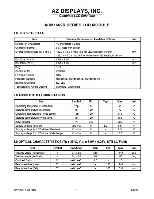
AZ DISPLAYS, INC.Complete LCD SolutionsACM1602R SERIES LCD MODULE1.0 PHYSICAL DATAItem Nominal Dimensions / Available Options Unit Number of Characters16 characters x 2 line-Character Format 5 x 7 dots with cursor-mm Overall Module Size (W x H x D)122.0 x 44.0 x max 14.5 for LED backlight version122.0 x 44.0 x max 9.5 for reflective or EL backlight versionDot Size (W x H)0.92 x 1.10mm Dot Pitch (W x H)0.98 x 1.16mm Duty1/16-Controller IC KS0066-LC Fluid Options STN-Polarizer Options Reflective, Transflective, Transmissive-Backlight Options EL, LED-Temperature Range Options Standard, Wide temp-2.0 ABSOLUTE MAXIMUM RATINGSItem Symbol Min Typ Max Unit Operating temperature (Standard)Top0-50°C Storage temperature (Standard)Tst-20-70°C Operating temperature (Wide temp)Top-20-+70°C Storage temperature (Wide temp)Tst-30-+80°C Input voltage V I V SS-V DD V Supply voltage for logic V DD-V SS0 5.0 6.5V Supply voltage for LCD drive (Standard)V DD-V O0- 6.5V Supply voltage for LCD drive (Wide temp)V DD-V O0-13.5V3.0 OPTICAL CHARACTERISTICS (Ta = 25°C, V DD = 5.0V ± 0.25V, STN LC Fluid)Item Symbol Condition Min Typ Max Unit Viewing angle (horizontal)θCr ≥ 2.0±30-±45deg Viewing angle (vertical)φCr ≥ 2.060-80deg Contrast Ratio Crφ=0°, θ=0° 4.5-10Response time (rise)Trφ=0°, θ=0°-120240ms Response time (fall)Tfφ=0°, θ=0°-155310ms4.0 ELECTRICAL CHARACTERISTICS (Ta = 25°C, V DD =5.0V ± 0.25V)Item Symbol Condition Min Typ Max Unit Supply voltage for LCD drive (Std temp)V DD-V O Ta = 25°C 4.8V Supply voltage for LCD drive (Wide temp)V DD-V O Ta = 25°C 6.1V Input voltage V I- 4.75 5.0 5.25V Input high voltage V IH- 2.2-V DD V Input low voltage V IL-0-0.6V Output high voltage V OH I OH=0.2mA 2.4--V Output low voltage V OL I OL=1.2mA--0.4V Supply current I DD V DD=5.0V- 3.0mA Input leakage current I LKG--- 1.0uA LED power supply current I LED V LED=5V, R=3.6Ω-220-mA EL power supply current I EL V EL=110V AC, 400H Z- 5.0-mA5.0 INTERFACE PIN CONNECTIONSPin No.Symbol Level Pin Description Function 1V SS-Ground0V2V DD-Supply voltage for logic+5V3V O-LCD contrast adjust By user4RS H/L Register select H: Data; L: Instruction code 5R/W H/L Read / write H: Data read, L: Data write 6E H, H→L Enable Start signal for data read/write 7DB0H/L Data bit 08-bit interface8DB1H/L Data bit 18-bit interface9DB2H/L Data bit 28-bit interface10DB3H/L Data bit 38-bit interface11DB4H/L Data bit 44-bit or 8-bit interface12DB5H/L Data bit 54-bit or 8-bit interface13DB6H/L Data bit 64-bit or 8-bit interface14DB7H/L Data bit 74-bit or 8-bit interface15A-Anode for LED backlight Power supply for LED/EL backlights 16K-Cathode for LED backlight Power supply for LED/EL backlights6.0 POWER SUPPLY7.0 BLOCK DIAGRAMStandard temp range V R = 10K Ω ~ 20K ΩWide temp range V R = 10K Ω ~ 20K Ω8.0 TIMING CHARACTERISTICS (KS0066 Controller)Item Symbol Test Condition Min.Typ.Max.Unit Enable cycle time t CYC Fig. a, Fig. b500--ns Enable pulse width PW EH Fig. a, Fig. b220--ns Enable rise/fall time t Er , t Ef Fig. a, Fig. b--25ns RS, R/W set up time t AS Fig. a, Fig. b40--ns RS, R/W hold time t H1Fig. a, Fig. b10--ns Data set up time t DSW Fig. a60--ns Data hold time t H2Fig. a10--nsData delay time t DDR Fig. b--120nsData hold time t H2Fig. b20--ns。
MX29LV160C T/B16M-BIT [2Mx8/1Mx16] CMOS SINGLE VOLTAGE3V ONLY FLASH MEMORY•Ready/Busy# pin (RY/BY#)- Provides a hardware method of detecting program or erase operation completion.•Sector protection- Hardware method to disable any combination of sectors from program or erase operations- Temporary sector unprotect allows code changes in previously locked sectors.•CFI (Common Flash Interface) compliant- Flash device parameters stored on the device and provide the host system to access•100,000 minimum erase/program cycles•Latch-up protected to 100mA from -1V to VCC+1V •Boot Sector Architecture - T = Top Boot Sector - B = Bottom Boot Sector•Low VCC write inhibit is equal to or less than 1.4V •Package type:- 44-pin SOP - 48-pin TSOP - 48-ball CSP- All Pb-free devices are RoHS Compliant •Compatibility with JEDEC standard- Pinout and software compatible with single-power supply Flash•10 years data retentionFEATURES•Extended single - supply voltage range 2.7V to 3.6V •2,097,152 x 8/1,048,576 x 16 switchable •Single power supply operation- 3.0V only operation for read, erase and program operation•Fully compatible with MX29LV160B device •Fast access time: 55R/70/90ns •Low power consumption- 30mA maximum active current - 0.2uA typical standby current •Command register architecture- Byte/word Programming (9us/11us typical)- Sector Erase (Sector structure 16K-Bytex1,8K-Bytex2, 32K-Bytex1, and 64K-Byte x31)•Auto Erase (chip & sector) and Auto Program- Automatically erase any combination of sectors with Erase Suspend capability.- Automatically program and verify data at specified address•Erase Suspend/Erase Resume- Suspends sector erase operation to read data from,or program data to, any sector that is not being erased,then resumes the erase.•Status Reply- Data# Polling & Toggle bit for detection of program and erase operation completion.GENERAL DESCRIPTIONThe MX29L V160C T/B is a 16-mega bit Flash memory organized as 2M bytes of 8 bits or 1M words of 16 bits.MXIC's Flash memories offer the most cost-effective and reliable read/write non-volatile random access memory. The MX29LV160C T/B is packaged in 44-pin SOP , 48-pin TSOP and 48-ball CSP . It is designed to be reprogrammed and erased in system or in standard EPROM programmers.The standard MX29LV160C T/B offers access time as fast as 55ns, allowing operation of high-speed micropro-cessors without wait states. To eliminate bus conten-tion, the MX29LV160C T/B has separate chip enable (CE#) and output enable (OE#) controls.MXIC's Flash memories augment EPROM functionality with in-circuit electrical erasure and programming. The MX29LV160C T/B uses a command register to manage this functionality. The command register allows for 100%TTL level control inputs and fixed power supply levels during erase and programming, while maintaining maxi-mum EPROM compatibility.MXIC Flash technology reliably stores memory contents even after 100,000 erase and program cycles. The MXIC cell is designed to optimize the erase and programming mechanisms. In addition, the combination of advanced tunnel oxide processing and low internal electric fields for erase and program operations produces reliable cy-cling. The MX29LV160C T/B uses a 2.7V~3.6V VCC supply to perform the High Reliability Erase and auto Program/Erase algorithms.The highest degree of latch-up protection is achieved with MXIC's proprietary non-epi process. Latch-up pro-tection is proved for stresses up to 100 milliamps on address and data pin from -1V to VCC + 1V.MX29LV160C T/BPIN CONFIGURATIONSPIN DESCRIPTIONSYMBOL PIN NAME A0~A19Address Input Q0~Q14Data Input/OutputQ15/A-1Q15(Word mode)/LSB addr(Byte mode)CE#Chip Enable Input WE#Write Enable Input BYTE#Word/Byte Selection input RESET#Hardware Reset Pin/Sector Protect UnlockOE#Output Enable Input RY/BY#Ready/Busy OutputVCC Power Supply Pin (2.7V~3.6V)GNDGround Pin48 TSOP (Standard Type) (12mm x 20mm)44 SOP(500 mil)A B C D E F GH6A13A12A14A15A16BYTE#Q15/A-1GND 5A9A8A10A11Q7Q14Q13Q64WE#RESET#NCA19Q5Q12VCC Q43RY/BY#NC A18NC Q2Q10Q11Q32A7A17A6A5Q0Q8Q9Q11A3A4A2A1A0CE#OE#GND48-Ball CSP 6mm x 8mm (Ball Pitch=0.8mm) Top View, Balls Facing Down234567891011121314151617181920212244434241403938373635343332313029282726252423RESET#A18A17A7A6A5A4A3A2A1A0CE#GND OE#Q0Q8Q1Q9Q2Q10Q3Q11WE#A19A8A9A10A11A12A13A14A15A16BYTE#GND Q15/A-1Q7Q14Q6Q13Q5Q12Q4VCCM X 29L V 160C T /BA15A14A13A12A11A10A9A8A19NC WE#RESET#NC NC RY/BY#A18A17A7A6A5A4A3A2A1123456789101112131415161718192021222324A16BYTE#GND Q15/A-1Q7Q14Q6Q13Q5Q12Q4VCC Q11Q3Q10Q2Q9Q1Q8Q0OE#GND CE#A0484746454443424140393837363534333231302928272625MX29LV160C T/BMX29LV160C T/BBLOCK STRUCTURETable 1: MX29LV160CT SECTOR ARCHITECTURESector Sector Size Address range Sector Address Byte Mode Word Mode Byte Mode(x8) Word Mode(x16)A19A18A17A16A15A14A13A12 SA064Kbytes32Kwords000000-00FFFF00000-07FFF00000X X X SA164Kbytes32Kwords010000-01FFFF08000-0FFFF00001X X X SA264Kbytes32Kwords020000-02FFFF10000-17FFF00010X X X SA364Kbytes32Kwords030000-03FFFF18000-1FFFF00011X X X SA464Kbytes32Kwords040000-04FFFF20000-27FFF00100X X X SA564Kbytes32Kwords050000-05FFFF28000-2FFFF00101X X X SA664Kbytes32Kwords060000-06FFFF30000-37FFF00110X X X SA764Kbytes32Kwords070000-07FFFF38000-3FFFF00111X X X SA864Kbytes32Kwords080000-08FFFF40000-47FFF01000X X X SA964Kbytes32Kwords090000-09FFFF48000-4FFFF01001X X X SA1064Kbytes32Kwords0A0000-0AFFFF50000-57FFF01010X X X SA1164Kbytes32Kwords0B0000-0BFFFF58000-5FFFF01011X X X SA1264Kbytes32Kwords0C0000-0CFFFF60000-67FFF01100X X X SA1364Kbytes32Kwords0D0000-0DFFFF68000-6FFFF01101X X X SA1464Kbytes32Kwords0E0000-0EFFFF70000-77FFF01110X X X SA1564Kbytes32Kwords0F0000-0FFFFF78000-7FFFF01111X X X SA1664Kbytes32Kwords100000-10FFFF80000-87FFF10000X X X SA1764Kbytes32Kwords110000-11FFFF88000-8FFFF10001X X X SA1864Kbytes32Kwords120000-12FFFF90000-97FFF10010X X X SA1964Kbytes32Kwords130000-13FFFF98000-9FFFF10011X X X SA2064Kbytes32Kwords140000-14FFFF A0000-A7FFF10100X X X SA2164Kbytes32Kwords150000-15FFFF A8000-AFFFF10101X X X SA2264Kbytes32Kwords160000-16FFFF B0000-B7FFF10110X X X SA2364Kbytes32Kwords170000-17FFFF B8000-BFFFF10111X X X SA2464Kbytes32Kwords180000-18FFFF C0000-C7FFF11000X X X SA2564Kbytes32Kwords190000-19FFFF C8000-CFFFF11001X X X SA2664Kbytes32Kwords1A0000-1AFFFF D0000-D7FFF11010X X X SA2764Kbytes32Kwords1B0000-1BFFFF D8000-DFFFF11011X X X SA2864Kbytes32Kwords1C0000-1CFFFF E0000-E7FFF11100X X X SA2964Kbytes32Kwords1D0000-1DFFFF E8000-EFFFF11101X X X SA3064Kbytes32Kwords1E0000-1EFFFF F0000-F7FFF11110X X X SA3132Kbytes16Kwords1F0000-1F7FFF F8000-FBFFF111110X X SA328Kbytes4Kwords1F8000-1F9FFF FC000-FCFFF11111100 SA338Kbytes4Kwords1FA000-1FBFFF FD000-FDFFF11111101 SA3416Kbytes8Kwords1FC000-1FFFFF FE000-FFFFF1111111XNote: Byte mode: address range A19:A-1, word mode:address range A19:A0.MX29LV160C T/BTable 2: MX29LV160CB SECTOR ARCHITECTURESector Sector Size Address range Sector Address Byte Mode Word Mode Byte Mode (x8)Word Mode (x16)A19A18A17A16A15A14A13A12 SA016Kbytes8Kwords000000-003FFF00000-01FFF0000000X SA18Kbytes4Kwords004000-005FFF02000-02FFF00000010 SA28Kbytes4Kwords006000-007FFF03000-03FFF00000011 SA332Kbytes16Kwords008000-00FFFF04000-07FFF000001X X SA464Kbytes32Kwords010000-01FFFF08000-0FFFF00001X X X SA564Kbytes32Kwords020000-02FFFF10000-17FFF00010X X X SA664Kbytes32Kwords030000-03FFFF18000-1FFFF00011X X X SA764Kbytes32Kwords040000-04FFFF20000-27FFF00100X X X SA864Kbytes32Kwords050000-05FFFF28000-2FFFF00101X X X SA964Kbytes32Kwords060000-06FFFF30000-37FFF00110X X X SA1064Kbytes32Kwords070000-07FFFF38000-3FFFF00111X X X SA1164Kbytes32Kwords080000-08FFFF40000-47FFF01000X X X SA1264Kbytes32Kwords090000-09FFFF48000-4FFFF01001X X X SA1364Kbytes32Kwords0A0000-0AFFFF50000-57FFF01010X X X SA1464Kbytes32Kwords0B0000-0BFFFF58000-5FFFF01011X X X SA1564Kbytes32Kwords0C0000-0CFFFF60000-67FFF01100X X X SA1664Kbytes32Kwords0D0000-0DFFFF68000-6FFFF01101X X X SA1764Kbytes32Kwords0E0000-0EFFFF70000-77FFF01110X X X SA1864Kbytes32Kwords0F0000-0FFFFF78000-7FFFF01111X X X SA1964Kbytes32Kwords100000-10FFFF80000-87FFF10000X X X SA2064Kbytes32Kwords110000-11FFFF88000-8FFFF10001X X X SA2164Kbytes32Kwords120000-12FFFF90000-97FFF10010X X X SA2264Kbytes32Kwords130000-13FFFF98000-9FFFF10011X X X SA2364Kbytes32Kwords140000-14FFFF A0000-A7FFF10100X X X SA2464Kbytes32Kwords150000-15FFFF A8000-AFFFF10101X X X SA2564Kbytes32Kwords160000-16FFFF B0000-B7FFF10110X X X SA2664Kbytes32Kwords170000-17FFFF B8000-BFFFF10111X X X SA2764Kbytes32Kwords180000-18FFFF C0000-C7FFF11000X X X SA2864Kbytes32Kwords190000-19FFFF C8000-CFFFF11001X X X SA2964Kbytes32Kwords1A0000-1AFFFF D0000-D7FFF11010X X X SA3064Kbytes32Kwords1B0000-1BFFFF D8000-DFFFF11011X X X SA3164Kbytes32Kwords1C0000-1CFFFF E0000-E7FFF11100X X X SA3264Kbytes32Kwords1D0000-1DFFFF E8000-EFFFF11101X X X SA3364Kbytes32Kwords1E0000-1EFFFF F0000-FFFFF11110X X X SA3464Kbytes32Kwords1F0000-1FFFFF F8000-FFFFF11111X X XNote: Byte mode:address range A19:A-1, word mode:address range A19:A0.MX29LV160C T/BBLOCK DIAGRAMCONTROL INPUT LOGICPROGRAM/ERASE HIGH VOLTAGEWRITE STATE MACHINE (WSM)STATE REGISTERFLASH ARRAYX-DECODERADDRESS LATCHAND BUFFERY -PASS GATEY -DECODERARRAY SOURCE HVCOMMAND DATADECODERCOMMAND DATA LATCHI/O BUFFERPGM DATA HVPROGRAM DATA LATCHSENSE AMPLIFIERQ0-Q15/A-1A0-A19CE#OE#WE#RESET#MX29LV160C T/BAUTOMATIC PROGRAMMINGThe MX29L V160C T/B is byte/word programmable using the Automatic Programming algorithm. The Automatic Programming algorithm makes the external system do not need to have time out sequence nor to verify the data programmed. The typical chip programming time at room temperature of the MX29LV160C T/B is less than 18 sec (byte)/12 sec (word).AUTOMATIC PROGRAMMING ALGORITHMMXIC's Automatic Programming algorithm requires the user to only write program set-up commands (including 2 unlock write cycle and A0H) and a program command (program data and address). The device automatically times the programming pulse width, provides the pro-gram verification, and counts the number of sequences.A status bit similar to Data# Polling and a status bit toggling between consecutive read cycles, provide feed-back to the user as to the status of the programming operation. Refer to write operation status, table 7, for more information on these status bits.AUTOMATIC CHIP ERASEThe entire chip is bulk erased using 10 ms erase pulses according to MXIC's Automatic Chip Erase algorithm. T ypical erasure at room temperature is accomplished in less than 25 second. The Automatic Erase algorithm automatically programs the entire array prior to electrical erase. The timing and verification of electrical erase are controlled internally within the device.AUTOMATIC SECTOR ERASEThe MX29L V160C T/B is sector(s) erasable using MXIC's Auto Sector Erase algorithm. The Automatic Sector Erase algorithm automatically programs the specified sector(s) prior to electrical erase. The timing and verifi-cation of electrical erase are controlled internally within the device. An erase operation can erase one sector, multiple sectors, or the entire device.AUTOMATIC ERASE ALGORITHMMXIC's Automatic Erase algorithm requires the user to write commands to the command register using stan-dard microprocessor write timings. The device will auto-matically pre-program and verify the entire array. Then the device automatically times the erase pulse width, provides the erase verification, and counts the number of sequences. A status bit toggling between consecutive read cycles provides feedback to the user as to the sta-tus of the erasing operation.Register contents serve as inputs to an internal state-machine which controls the erase and programming cir-cuitry. During write cycles, the command register inter-nally latches address and data needed for the program-ming and erase operations. During a system write cycle, addresses are latched on the falling edge, and data are latched on the rising edge of WE# or CE#, whichever happens first.MXIC's Flash technology combines years of EPROM experience to produce the highest levels of quality, reli-ability, and cost effectiveness. The MX29LV160C T/B electrically erases all bits simultaneously using Fowler-Nordheim tunneling. The bytes are programmed by us-ing the EPROM programming mechanism of hot electron injection.During a program cycle, the state-machine will control the program sequences and command register will not respond to any command set. During a Sector Erase cycle, the command register will only respond to Erase Suspend command. After Erase Suspend is completed, the device stays in read mode. After the state machine has completed its task, it will allow the command regis-ter to respond to its full command set.AUTOMATIC SELECTThe automatic select mode provides manufacturer and device identification, and sector protection verification, through identifier codes output on Q7~Q0. This mode is mainly adapted for programming equipment on the de-vice to be programmed with its programming algorithm. When programming by high voltage method, automatic select mode requires VID (11.5V to 12.5V) on address pin A9. Other address pin A6, A1 and A0 as referring to T able 3. In addition, to access the automatic select codes in-system, the host can issue the automatic select com-mand through the command register without requiring VID, as shown in table 5.To verify whether or not sector being protected, the sec-tor address must appear on the appropriate highest orderMX29LV160C T/BA19A11A9A8A6A5A1A0Description Mode CE#OE#WE#RESET# || | |Q15~Q0A12A10A7A2Read Silicon ID LLHHXXVID XL XLLC2HManufacture Code Device ID Word L L H H X X VID X L X L H 22C4H (Top Boot Block)Byte L L H H X X VID X L X L H XXC4H Device IDWordL L H H X X VID X L X L H 2249H (Bottom Boot Block)ByteL L H H X X VID X L X L H XX49H XX01HSector Protection LLHHSAXVIDXLXHL(protected)VerificationXX00H(unprotected)TABLE 3. MX29LV160C T/B AUTO SELECT MODE BUS OPERATION (A9=VID)NOTE: SA=Sector Address, X=Don't Care, L=Logic Low, H=Logic Highaddress bit (see T able 1 and T able 2). The rest of address bits, as shown in T able 3, are don't care. Once all neces-sary bits have been set as required, the programming equipment may read the corresponding identifier code on Q7~Q0.MX29LV160C T/BQUERY COMMAND AND COMMON FLASH INTERFACE (CFI) MODEMX29L V160C T/B is capable of operating in the CFI mode. This mode all the host system to determine the manu-facturer of the device such as operating parameters and configuration. T wo commands are required in CFI mode. Query command of CFI mode is placed first, then the Reset command exits CFI mode. These are described in T able 4.The single cycle Query command is valid only when the device is in the Read mode, including Erase Suspend, Standby mode, and Automatic Select mode; however, it is ignored otherwise.The Reset command exits from the CFI mode to the Read mode, or Erase Suspend mode, or Automatic Se-lect mode. The command is valid only when the device is in the CFI mode.Table 4-1. CFI mode: Identification Data Values(All values in these tables are in hexadecimal)Description Address Address Data(Byte Mode)(Word Mode) Query-unique ASCII string "QRY"201000512211005224120059 Primary vendor command set and control interface ID code2613000228140000 Address for primary algorithm extended query table2A1500402C160000 Alternate vendor command set and control interface ID code (none)2E17000030180000 Address for secondary algorithm extended query table (none)32190000341A0000 Table 4-2. CFI Mode: System Interface Data Values(All values in these tables are in hexadecimal)Description Address Address Data(Byte Mode)(Word Mode) VCC supply, minimum (2.7V)361B0027 VCC supply, maximum (3.6V)381C0036 VPP supply, minimum (none)3A1D0000 VPP supply, maximum (none)3C1E0000 Typical timeout for single word/byte write (2N us)3E1F0004 Typical timeout for Minimum size buffer write (2N us) (not supported)40200000 Typical timeout for individual sector erase (2N ms)4221000A Typical timeout for full chip erase (2N ms)44220000 Maximum timeout for single word/byte write times (2N X Typ)46230005 Maximum timeout for buffer write times (2N X Typ)48240000 Maximum timeout for individual sector erase times (2N X Typ)4A250004 Maximum timeout for full chip erase times (not supported)4C260000MX29LV160C T/B Table 4-3. CFI Mode: Device Geometry Data Values(All values in these tables are in hexadecimal)Description Address Address Data(Byte Mode)(Word Mode) Device size (2N bytes)4E270015 Flash device interface code (x8/x16 async.)5028000252290000 Maximum number of bytes in multi-byte write (not supported)542A0000562B0000 Number of erase sector regions582C0004 Erase sector region 1 information (refer to the CFI publication 100)5A2D00005C2E00005E2F004060300000 Erase sector region 2 information62310001643200006633002068340000 Erase sector region 3 information6A3500006C3600006E37008070380000 Erase sector region 4 information7239001E743A0000763B0000783C0001 Table 4-4. CFI Mode: Primary Vendor-Specific Extended Query Data Values(All values in these tables are in hexadecimal)Description Address Address Data(Byte Mode)(Word Mode) Query-unique ASCII string "PRI"804000508241005284420049 Major version number, ASCII86430031 Minor version number, ASCII88440030 Address sensitive unlock (0=required, 1= not required)8A450000 Erase suspend (2= to read and write)8C460002 Sector protect (N= # of sectors/group)8E470001 Temporary sector unprotect (1=supported)90480001 Sector protect/chip unprotect scheme92490004 Simultaneous R/W operation (0=not supported)944A0000 Burst mode type (0=not supported)964B0000 Page mode type (0=not supported)984C0000MX29LV160C T/Bin the improper sequence will reset the device to the read mode. Table 5 defines the valid register command sequences. Note that the Erase Suspend (B0H) and Erase Resume (30H) commands are valid only while the Sector Erase operation is in progress.COMMAND DEFINITIONSDevice operations are selected by writing specific ad-dress and data sequences into the command register.Writing incorrect address and data values or writing them First Bus Second Bus Third Bus Fourth Bus Fifth Bus Sixth Bus CommandBusCycleCycleCycleCycleCycle CycleCycle AddrData Addr Data Addr Data Addr DataAddrData Addr DataReset 1XXXH F0H Read1RARDRead Silicon IDWord 4555H AAH 2AAH 55H 555H 90H ADI DDI Byte4AAAH AAH 555H 55H AAAH 90H ADI DDI Sector Protect Word4555H AAH 2AAH55H555H90H (SA)XX00H Verifyx02HXX01H Byte4AAAH AAH 555H55HAAAH90H (SA)00H x04H01H Program Word 4555H AAH 2AAH 55H 555H A0H PA PD Byte4AAAH AAH 555H 55H AAAH A0H PAPDChip Erase Word 6555H AAH 2AAH 55H 555H 80H 555H AAH 2AAH 55H 555H 10H Byte6AAAH AAH 555H 55H AAAH 80H AAAH AAH 555H 55H AAAH 10H Sector Erase Word 6555H AAH 2AAH 55H 555H 80H 555H AAH 2AAH 55H SA 30H Byte6AAAH AAH 555H 55HAAAH80H AAAH AAH555H 55HSA30HSector Erase Suspend 1XXXH B0H Sector Erase Resume 1XXXH 30H CFI QueryWord 155H 98ByteAAHTABLE 5. MX29L V160C T/B COMMAND DEFINITIONSNote:1. ADI = Address of Device identifier; A1=0, A0 = 0 for manufacturer code,A1=0, A0 = 1 for device code. A2-A19=do not care. (Refer to table 3)DDI = Data of Device identifier : C2H for manufacture code, C4H/49H (x8) and 22C4H/2249H (x16) for device code. X = X can be VIL or VIHRA=Address of memory location to be read. RD=Data to be read at location RA.2.PA = Address of memory location to be programmed. PD = Data to be programmed at location PA. SA = Address of the sector to be erased.3.The system should generate the following address patterns: 555H or 2AAH to Address A10~A0 in word mode/AAAH or 555H to Address A10~A-1 in byte mode.Address bit A11~A19=X=Don't care for all address commands except for Program Address (P A) and Sector Address (SA). Write Sequence may be initiated with A11~A19 in either state.4. For Sector Protect Verify operation: If read out data is 01H, it means the sector has been protected. If read out data is 00H,it means the sector is still not being protected.5. Any number of CFI data read cycles are permitted.MX29LV160C T/BTABLE 6. MX29L V160C T/B BUS OPERATIONADDRESS Q8~Q15 DESCRIPTION CE#OE#WE#RE- A19A11A9A8A6A5A1A0Q0~Q7BYTE BYTESET#A12A10A7A2=VIH=VIL Read L L H H AIN Dout Dout Q8~Q14=High ZQ15=A-1 Write L H L H AIN DIN(3)DINReset X X X L X High Z High Z High Z Temporary sector unlock X X X VID AIN DIN DIN High Z Output Disable L H H H X High Z High Z High Z Standby Vcc±X X Vcc±X High Z High Z High Z0.3V0.3VSector Protect L H L VID SA X X X L X H L DIN X XChip Unprotect L H L VID X X X X H X H L DIN X X Sector Protection Verify L L H H SA X VID X L X H L CODE(5)X XNOTES:1.Manufacturer and device codes may also be accessed via a command register write sequence. Refer to T able 4.2. VID is the high voltage, 11.5V to 12.5V.3.Refer to T able 5 for valid Data-In during a write operation.4.X can be VIL or VIH.5.Code=00H/XX00H means unprotected.Code=01H/XX01H means protected.6.A19~A12=Sector address for sector protect.7.The sector protect and chip unprotect functions may also be implemented via programming equipment.MX29LV160C T/BREQUIREMENTS FOR READING ARRAY DATAT o read array data from the outputs, the system must drive the CE# and OE# pins to VIL. CE# is the power control and selects the device. OE# is the output control and gates array data to the output pins. WE# should re-main at VIH.The internal state machine is set for reading array data upon device power-up, or after a hardware reset. This ensures that no spurious alteration of the memory con-tent occurs during the power transition. No command is necessary in this mode to obtain array data. Standard microprocessor read cycles that assert valid address on the device address inputs produce valid data on the device data outputs. The device remains enabled for read access until the command register contents are altered. WRITE COMMANDS/COMMAND SEQUENCESTo program data to the device or erase sectors of memory, the system must drive WE# and CE# to VIL, and OE# to VIH.An erase operation can erase one sector, multiple sec-tors, or the entire device. T able 1 and T able 2 indicate the address space that each sector occupies. A "sector ad-dress" consists of the address bits required to uniquely select a sector. The Writing specific address and data commands or sequences into the command register ini-tiates device operations. Table 5 defines the valid regis-ter command sequences. Writing incorrect address and data values or writing them in the improper sequence resets the device to reading array data. Section has de-tails on erasing a sector or the entire chip, or suspend-ing/resuming the erase operation.After the system writes the "read silicon-ID" and "sector protect verify" command sequence, the device enters the "read silicon-ID" and "sector protect verify" mode. The system can then read "read silicon-ID" and "sector protect verify" codes from the internal register (which is separate from the memory array) on Q7-Q0. Standard read cycle timings apply in this mode. Refer to the "read silicon-ID" and "sector protect verify" Mode and "read silicon-ID" and "sector protect verify" Command Se-quence section for more information.ICC2 in the DC Characteristics table represents the ac-tive current specification for the write mode. The "AC Characteristics" section contains timing specification table and timing diagrams for write operations. STANDBY MODEWhen using both pins of CE# and RESET#, the device enter CMOS Standby with both pins held at Vcc ± 0.3V. If CE# and RESET# are held at VIH, but not within the range of VCC ± 0.3V, the device will still be in the standby mode, but the standby current will be larger. During Auto Algorithm operation, Vcc active current (ICC2) is required even CE# = "H" until the operation is completed. The device can be read with standard access time (tCE) from either of these standby modes, before it is ready to read data.OUTPUT DISABLEWith the OE# input at a logic high level (VIH), output from the devices are disabled. This will cause the output pins to be in a high impedance state.RESET# OPERATIONThe RESET# pin provides a hardware method of reset-ting the device to reading array data. When the RESET# pin is driven low for at least a period of tRP, the device immediately terminates any operation in progress, tristates all output pins, and ignores all read/write com-mands for the duration of the RESET# pulse. The device also resets the internal state machine to reading array data. The operation that was interrupted should be re-initiated once the device is ready to accept another com-mand sequence, to ensure data integrity.Current is reduced for the duration of the RESET# pulse. When RESET# is held at VSS±0.3V, the device draws CMOS standby current (ICC4). If RESET# is held at VIL but not within VSS±0.3V, the standby current will be greater.The RESET# pin may be tied to system reset circuitry.A system reset would that also reset the Flash memory, enabling the system to read the boot-up firmware from the Flash memory.If RESET# is asserted during a program or erase opera-tion, the RY/BY# pin remains a "0" (busy) until the inter-MX29LV160C T/Bnal reset operation is complete, which requires a time of tREADY (during Embedded Algorithms). The system can thus monitor RY/BY# to determine whether the reset op-eration is complete. If RESET# is asserted when a pro-gram or erase operation is completed within a time of tREADY (not during Embedded Algorithms). The system can read data tRH after the RESET# pin returns to VIH. Refer to the AC Characteristics tables for RESET# pa-rameters and to Figure 22 for the timing diagram.READ/RESET COMMANDThe read or reset operation is initiated by writing the read/ reset command sequence into the command register. Microprocessor read cycles retrieve array data. The de-vice remains enabled for reads until the command regis-ter contents are altered.If program-fail or erase-fail happen, the write of F0H will reset the device to abort the operation. A valid com-mand must then be written to place the device in the desired state.SILICON-ID READ COMMANDFlash memories are intended for use in applications where the local CPU alters memory contents. As such, manu-facturer and device codes must be accessible while the device resides in the target system. PROM program-mers typically access signature codes by raising A9 to a high voltage (VID). However, multiplexing high voltage onto address lines is not generally desired system de-sign practice.The MX29LV160C T/B contains a Silicon-ID-Read op-eration to supple traditional PROM programming meth-odology. The operation is initiated by writing the read silicon ID command sequence into the command regis-ter. Following the command write, a read cycle with A1=VIL, A0=VIL retrieves the manufacturer code of C2H/ 00C2H. A read cycle with A1=VIL, A0=VIH returns the device code of C4H/22C4H for MX29L V160CT, 49H/2249H for MX29L V160CB.The system must write the reset command to exit the "Silicon-ID Read Command" code.AUTOMATIC CHIP ERASE COMMANDSChip erase is a six-bus cycle operation. There are two "unlock" write cycles. These are followed by writing the "set-up" command 80H. T wo more "unlock" write cycles are then followed by the chip erase command 10H. The device does not require the system to entirely pre-program prior to executing the Automatic Chip Erase. Upon executing the Automatic Chip Erase, the device will automatically program and verify the entire memory for an all-zero data pattern. When the device is auto-matically verified to contain an all-zero pattern, a self-timed chip erase and verify begin. The erase and verify operations are completed when the data on Q7 is "1" at which time the device returns to the Read mode. The system is not required to provide any control or timing during these operations.When using the Automatic Chip Erase algorithm, note that the erase automatically terminates when adequate erase margin has been achieved for the memory array (no erase verification command is required).If the Erase operation was unsuccessful, the data on Q5 is "1" (see Table 8), indicating the erase operation ex-ceed internal timing limit.The automatic erase begins on the rising edge of the last WE# or CE# pulse, whichever happens first in the com-mand sequence and terminates when either the data on Q7 is "1" at which time the device returns to the Read mode or the data on Q6 stops toggling for two consecu-tive read cycles at which time the device returns to the Read mode.。
T JMAX = 125°C, θJA = 150°C/W EXPOSED PAD (PIN 11) IS GND MUST BE SOLDERED TO PCB12345A IN +A IN –V REF GND GND 109876CONV SCK SDO V DD GNDTOP VIEW11MSE PACKAGE10-LEAD PLASTIC MSOP (Notes 1, 2)Supply Voltage (V DD ).................................................4V Analog Input Voltage(Note 3)....................................–0.3V to (V DD + 0.3V)Digital Input Voltage ................... – 0.3V to (V DD + 0.3V)Digital Output Voltage..................–0.3V to (V DD + 0.3V)Power Dissipation..............................................100mW Operation Temperature RangeLTC1403C-1/LTC1403AC-1.....................0°C to 70°C LTC1403I-1/LTC1403AI-1..................–40°C to 85°C Storage Temperature Range.................–65°C to 150°C Lead Temperature (Soldering, 10 sec)..................300°CORDER PART NUMBERMSE PART MARKINGLTBGP LTBGQ LTBGR LTBGSLTC1403CMSE-1LTC1403IMSE-1LTC1403ACMSE-1LTC1403AIMSE-1The q denotes the specifications which apply over the full operatingtemperature range, otherwise specifications are at T A = 25°C. With internal reference. V DD = 3VLTC1403-1LTC1403A-1PARAMETERCONDITIONSMIN TYP MAXMIN TYP MAX UNITS Resolution (No Missing Codes)q 1214Bits Integral Linearity Error (Notes 4, 5, 18)q –2±0.252–4±0.54LSB Offset Error (Notes 4, 18)q –10±110–20±220LSB Gain Error (Note 4, 18)q–30±530–60±1060LSB Gain TempcoInternal Reference (Note 4)±15±15ppm/°C External Reference±1±1ppm/°CThe q denotes the specifications which apply over the full operating temperature range,otherwise specifications are at T A = 25°C. V DD = 3VSYMBOL PARAMETER CONDITIONS MIN TYP MAX UNITSV IN Analog Differential Input Range (Notes 3, 8, 9) 2.7V ≤ V DD ≤ 3.3Vq–1.25 to 1.25V V CM Analog Common Mode + Differential 0 to V DDVInput Range (Note 10)I IN Analog Input Leakage Current q 1µA C IN Analog Input Capacitance 13pF t ACQ Sample-and-Hold Acquisition Time (Note 6)q39ns t AP Sample-and-Hold Aperture Delay Time 1ns t JITTER Sample-and-Hold Aperture Delay Time Jitter 0.3ps CMRRAnalog Input Common Mode Rejection Ratiof IN = 1MHz, V IN = 0V to 3V –60dB f IN = 100MHz, V IN = 0V to 3V–15dBConsult LTC Marketing for parts specified with wider operating temperature ranges.ABSOLUTE AXI U RATI GSW W WU PACKAGE/ORDER I FOR ATIOU U WCO VERTER CHARACTERISTICSUA ALOG I PUTUU14031fThe q denotes the specifications which apply over the full operating temperature range,otherwise specifications are at T A = 25°C. V DD = 3V. Single-ended A IN + signal drive with A IN – = 1.5V DC. Differential signal drive with V CM = 1.5V at A IN + and A IN –LTC1403-1LTC1403A-1SYMBOL PARAMETER CONDITIONSMIN TYP MAX MIN TYP MAX UNITS SINADSignal-to-Noise Plus 100kHz Input Signal (Note 19)70.573.5dB Distortion Ratio1.4MHz Input Signal (Note 19)q6870.57073.5dB 100kHz Input Signal, External V REF = 3.3V,7276.3dB V DD ≥ 3.3V (Note 19)750kHz Input Signal, External V REF = 3.3V,7276.3dB V DD ≥ 3.3V (Note 19)THD Total Harmonic 100kHz First 5 Harmonics (Note 19)–87–90dB Distortion 1.4MHz First 5 Harmonics (Note 19)q –83–76–86–78dB SFDR Spurious Free 100kHz Input Signal (Note 19)–87–90dB Dynamic Range 1.4MHz Input Signal (Note 19)–83–86dB IMDIntermodulation 0.625V P-P 1.4MHz Summed with 0.625V P-P –82–82dB Distortion 1.56MHz into A IN + and Inverted into A IN –Code-to-Code V REF = 2.5V (Note 18)0.251LSB RMSTransition Noise Full Power Bandwidth V IN = 2.5V P-P , SDO = 11585LSB P-P (Note 15)5050MHz Full Linear BandwidthS/(N + D) ≥ 68dB55MHzThe q denotes the specifications which apply over thefull operating temperature range, otherwise specifications are at T A = 25°C. V DD = 3VPARAMETER CONDITIONS MINTYP MAXUNITSV REF Output Voltage I OUT = 02.5V V REF Output Tempco 15ppm/°C V REF Line Regulation V DD = 2.7V to 3.6V, V REF = 2.5V 600µV/V V REF Output Resistance Load Current = 0.5mA0.2ΩV REF Settling Time2msThe q denotes the specifications which apply over thefull operating temperature range, otherwise specifications are at T A = 25°C. V DD = 3VSYMBOL PARAMETERCONDITIONS MINTYP MAX UNITSV IH High Level Input Voltage V DD = 3.3V q 2.4V V IL Low Level Input Voltage V DD = 2.7V q 0.6V I IN Digital Input Current V IN = 0V to V DD q±10µA C IN Digital Input Capacitance (Note 20)5pF V OH High Level Output Voltage V DD = 3V, I OUT = –200µA q 2.5 2.9V V OL Low Level Output Voltage V DD = 2.7V, I OUT = 160µA 0.05V V DD = 2.7V, I OUT = 1.6mA q 0.100.4V I OZ Hi-Z Output Leakage D OUT V OUT = 0V to V DDq±10µA C OZ Hi-Z Output Capacitance D OUT 1pF I SOURCE Output Short-Circuit Source Current V OUT = 0V, V DD = 3V 20mA I SINKOutput Short-Circuit Sink CurrentV OUT = V DD = 3V 15mADY A IC ACCURACYUW I TER AL REFERE CE CHARACTERISTICSU U UDIGITAL I PUTS A D DIGITAL OUTPUTSUUSYMBOL PARAMETERCONDITIONSMIN TYP MAXUNITS f SAMPLE(MAX)Maximum Sampling Frequency per Channel q 2.8MHz (Conversion Rate)t THROUGHPUT Minimum Sampling Period (Conversion + Acquisiton Period)q357ns t SCK Clock Period (Note 16)q19.810000nst CONV Conversion Time(Note 6)1618SCLK cyclest 1Minimum Positive or Negative SCLK Pulse Width (Note 6)2ns t 2CONV to SCK Setup Time(Notes 6, 10)3ns t 3Nearest SCK Edge Before CONV(Note 6)0ns t 4Minimum Positive or Negative CONV Pulse Width (Note 6)4ns t 5SCK to Sample Mode (Note 6)4ns t 6CONV to Hold Mode(Notes 6, 11) 1.2ns t 716th SCK ↑ to CONV ↑ Interval (Affects Acquisition Period)(Notes 6, 7, 13)45ns t 8Minimum Delay from SCK to Valid Data (Notes 6, 12)8ns t 9SCK to Hi-Z at SDO(Notes 6, 12)6ns t 10Previous SDO Bit Remains Valid After SCK(Notes 6, 12)2ns t 12V REF Settling Time After Sleep-to-Wake Transition(Notes 6, 14)2msTI I G CHARACTERISTICSWU The q denotes the specifications which apply over the full operating temperaturerange, otherwise specifications are at T A = 25°C. V DD = 3VPOWER REQUIRE E T SWU The q denotes the specifications which apply over the full operating temperaturerange, otherwise specifications are at T A = 25°C. (Note 17)SYMBOL PARAMETER CONDITIONSMIN TYP MAX UNITSV DD Supply Voltage2.73.6V I DDPositive Supply VoltageActive Mode q 4.77mA Nap Modeq1.1 1.5mA Sleep Mode (LTC1403)215µA Sleep Mode (LTC1403A)210µA P DPower DissipationActive Mode with SCK in Fixed State (Hi or Lo)12mWNote 1: Absolute Maximum Ratings are those values beyond which the life of a device may be impaired.Note 2: All voltage values are with respect to GND.Note 3: When these pins are taken below GND or above V DD , they will be clamped by internal diodes. This product can handle input currents greater than 100mA below GND or greater than V DD without latchup.Note 4: Offset and full-scale specifications are measured for a single-ended A IN + input with A IN – grounded and using the internal 2.5V reference.Note 5: Integral linearity is tested with an external 2.55V reference and is defined as the deviation of a code from the straight line passing through the actual endpoints of a transfer curve. The deviation is measured from the center of quantization band.Note 6: Guaranteed by design, not subject to test.Note 7: Recommended operating conditions.Note 8: The analog input range is defined for the voltage differencebetween A IN + and A IN –. Performance is specified with A IN – = 1.5V DC while driving A IN +.Note 9: The absolute voltage at A IN + and A IN – must be within this range.Note 10: If less than 3ns is allowed, the output data will appear one clock cycle later. It is best for CONV to rise half a clock before SCK, when running the clock at rated speed.Note 11: Not the same as aperture delay. Aperture delay is smaller (1ns)because the 2.2ns delay through the sample-and-hold is subtracted from the CONV to Hold mode delay.Note 12: The rising edge of SCK is guaranteed to catch the data coming out into a storage latch.Note 13: The time period for acquiring the input signal is started by the 16th rising clock and it is ended by the rising edge of convert.Note 14: The internal reference settles in 2ms after it wakes up from Sleep mode with one or more cycles at SCK and a 10µF capacitive load.Note 15: The full power bandwidth is the frequency where the output code swing drops to 3dB with a 2.5V P-P input sine wave.Note 16: Maximum clock period guarantees analog performance during conversion. Output data can be read without an arbitrarily long clock.Note 17: V DD = 3V, f SAMPLE = 2.8Msps.Note 18: The LTC1403A-1 is measured and specified with 14-bitResolution (1LSB = 152µV) and the LTC1403-1 is measured and specified with 12-bit Resolution (1LSB = 610µV).Note 19: Full-scale sinewaves are fed into the noninverting input while the inverting input is kept at 1.5V DC.Note 20: The sampling capacitor at each input accounts for 4.1pF of the input capacitance.DRIVING THE ANALOG INPUTThe differential analog inputs of the LTC1403-1/LTC1403A-1are easy to drive. The inputs may be driven differentially or as a single-ended input (i.e., the A IN – input is set to V CM ). Both differential analog inputs, A IN + with A IN –, are sampled at the same instant. Any unwanted signal that is common to both inputs of each input pair will be reduced by the common mode rejection of the sample-and-hold circuit. The inputs draw only one small current spike while charging the sample-and-hold capacitors at the end of conversion. During conversion, the analog inputs draw only a small leakage current. If the source impedance of the driving circuit is low, then the LTC1403-1/LTC1403A-1 inputs can be driven directly. As source imped-ance increases, so will acquisition time. For minimum acqui-sition time with high source impedance, a buffer amplifier must be used. The main requirement is that the amplifier driving the analog input(s) must settle after the small current spike before the next conversion starts (settling time must be 39ns for full throughput rate). Also keep in mind while choosing an input amplifier, the amount of noise and har-monic distortion added by the amplifier.CHOOSING AN INPUT AMPLIFIERChoosing an input amplifier is easy if a few requirements are taken into consideration. First, to limit the magnitude of the voltage spike seen by the amplifier from charging the sam-pling capacitor, choose an amplifier that has a low output impedance (<100Ω) a t t he c losed-loop b andwidth f requency.For example, if an amplifier is used with a gain of 1 and has a unity-gain bandwidth of 50MHz, then the output impedance at 50MHz must be less than 100Ω. The second requirement is that the closed-loop bandwidth must be greater than 40MHz to ensure adequate small-signal settling for full throughput rate. If slower op amps are used, more time for settling can be provided by increasing the time between conversions. The best choice for an op amp to drive the LTC1403-1/LTC1403A-1 w ill d epend o n t he a pplication. G en-erally, applications fall into two categories: AC applications where dynamic specifications are most critical and time domain applications where DC accuracy and settling time are most critical. The following list is a summary of the op amps that are suitable for driving the LTC1403-1/LTC1403A-1.(More detailed information is available in the Linear Technol-ogy Databooks and our website at .)LTC ®1566-1: Low Noise 2.3MHz Continuous Time Low-Pass Filter.LT1630: Dual 30MHz Rail-to-Rail Voltage FB Amplifier. 2.7V to ±15V supplies. Very high A VOL , 500µV offset and 520ns settling to 0.5LSB for a 4V swing. THD and noise are –93dB to 40kHz and below 1LSB to 320kHz (A V = 1, 2V P-P into 1k Ω,V S = 5V), making the part excellent for AC applications (to 1/3 Nyquist) where rail-to-rail performance is desired. Quad version is available as LT1631.LT1632: Dual 45MHz Rail-to-Rail Voltage FB Amplifier. 2.7V to ±15V supplies. Very high A VOL , 1.5mV offset and 400ns settling to 0.5LSB for a 4V swing. It is suitable for applica-tions with a single 5V supply. THD and noise are –93dB to 40kHz and below 1LSB to 800kHz (A V = 1,2V P-P into 1k Ω, V S = 5V), making the part excellent for AC applications where rail-to-rail performance is desired. Quad version is available as LT1633.LT1813: Dual 100MHz 750V/µs 3mA Voltage Feedback Amplifier. 5V to ±5V supplies. Distortion is –86dB to 100kHz and –77dB to 1MHz with ±5V supplies (2V P-P into 500Ω).Excellent part for fast AC applications with ±5V␣supplies.LT1801: 80MHz GBWP, –75dBc at 500kHz, 2mA/Amplifier,8.5nV/√Hz.LT1806/LT1807: 325MHz G BWP, –80dBc D istortion a t 5MHz,Unity-Gain S table, R -R I n a nd O ut, 10mA/Amplifier, 3.5nV/√Hz.LT1810: 180MHz GBWP, –90dBc Distortion at 5MHz,Unity-Gain S table, R -R I n a nd O ut, 15mA/Amplifier, 16nV/√Hz.LT1818/LT1819: 400MHz, 2500V/µs,9mA, Single/Dual Volt-age Mode Operational Amplifier.LT6200: 165MHz GBWP, –85dBc Distortion at 1MHz, Unity-Gain Stable, R-R In and Out, 15mA/Amplifier,0.95nV/√Hz.LT6203: 100MHz GBWP, –80dBc Distortion at 1MHz,Unity-Gain Stable, R-R In and Out, 3mA/Amplifier,1.9nV/√Hz.LT6600-10: Amplifier/Filter Differential In/Out with 10MHz Cutoff.APPLICATIO S I FOR ATIOW UUU111214031 F07Figure 7. Recommended LayoutDigital circuitry grounds must be connected to the digital supply common. In applications where the ADC data outputs and control signals are connected to a continu-ously active microprocessor bus, it is possible to get errors in the conversion results. These errors are due to feedthrough from the microprocessor to the successive131414031fmode and the power drain drops from 14mW to 6mW. The internal reference remains powered in Nap mode. One or more rising edges at SCK wake up the LTC1403-1/LTC1403A-1 for service very quickly, and CONV can start an accurate conversion within a clock cycle. Four rising edges at CONV, without any intervening rising edges at SCK, put the LTC1403-1/LTC1403A-1 in Sleep mode and the power drain drops from 16mW to 10µW. One or more rising edges at SCK wake up the LTC1403-1/LTC1403A-1for operation. The internal reference (V REF ) takes 2ms to slew and settle with a 10µF load. Note that, using sleep mode more frequently than every 2ms, compromises the settled accuracy of the internal reference. Note that, for slower conversion rates, the Nap and Sleep modes can be used for substantial reductions in power consumption.DIGITAL INTERFACEThe LTC1403-1/LTC1403A-1 has a 3-wire SPI (Serial Protocol Interface) interface. The SCK and CONV inputs and SDO output implement this interface. The SCK and CONV inputs accept swings from 3V logic and are TTL compatible, if the logic swing does not exceed V DD . A detailed description of the three serial port signals follows:Conversion Start Input (CONV)The rising edge of CONV starts a conversion, but subse-quent rising edges at CONV are ignored by the LTC1403-1/LTC1403A-1 until the following 16 SCK rising edges have occurred. It is necessary to have a minimum of 16 rising edges of the clock input SCK between rising edges of CONV. But to obtain maximum conversion speed, it is necessary to allow two more clock periods between con-versions to allow 39ns of acquisition time for the internal ADC sample-and-hold circuit. With 16 clock periods per conversion, the maximum conversion rate is limited to 2.8Msps to allow 39ns for acquisition time. In either case,the output data stream comes out within the first 16 clock periods to ensure compatibility with processor serial ports. The duty cycle of CONV can be arbitrarily chosen to be used as a frame sync signal for the processor serial port. A simple approach to generate CONV is to create a pulse that is one SCK wide to drive the LTC1403-1/LTC1403A-1 and then buffer this signal with the appropri-ate number of inverters to ensure the correct delay drivingthe frame sync input of the processor serial port. It is good practice to drive the LTC1403-1/LTC1403A-1 CONV input first to avoid digital noise interference during the sample-to-hold transition triggered by CONV at the start of conver-sion. It is also good practice to keep the width of the low portion of the CONV signal greater than 15ns to avoid introducing glitches in the front end of the ADC just before the sample-and-hold goes into hold mode at the rising edge of CONV.Minimizing Jitter on the CONV InputIn high speed applications where high amplitude sinewaves above 100kHz are sampled, the CONV signal must have as little jitter as possible (10ps or less). The square wave output of a common crystal clock module usually meets this requirement easily. The challenge is to generate a CONV signal from this crystal clock without jitter corrup-tion from other digital circuits in the system. A clock divider and any gates in the signal path from the crystal clock to the CONV input should not share the same integrated circuit with other parts of the system. As shown in the interface circuit examples, the SCK and CONV inputs should be driven first, with digital buffers used to drive the serial port interface. Also note that the master clock in the DSP may already be corrupted with jitter, even if it comes directly from the DSP crystal. Another problem with high speed processor clocks is that they often use a low cost,low speed crystal (i.e., 10MHz) to generate a fast, but jittery, phase-locked-loop system clock (i.e., 40MHz). The jitter in these PLL-generated high speed clocks can be several nanoseconds. Note that if you choose to use the frame sync signal generated by the DSP port, this signal will have the same jitter of the DSP’s master clock.Serial Clock Input (SCK)The rising edge of SCK advances the conversion process and also udpates each bit in the SDO data stream. After CONV rises, the third rising edge of SCK starts clocking out the 12/14 data bits with the MSB sent first. A simple approach is to generate SCK to drive the LTC1403-1/LTC1403A-1 first and then buffer this signal with the appropriate number of inverters to drive the serial clock input of the processor serial port. Use the falling edge of the clock to latch data from the Serial Data Output (SDO)APPLICATIO S I FOR ATIOW UUU151614031fAPPLICATIO S I FOR ATIOW UU U ; 10-23-03 ******************************************************************; Files: 014SI.ASM -> 1403 bipolar Sine wave collection with Serial Port interface ; bvectors.asm buffered mode.; s2k14ini.asm 2k buffer size.; first element at 1024, last element at 1023, two middles at 2047 and 0000; bipolar mode; Works 16 or 64 clock frames.; negative edge BCLKR ; negative BFSR pulse ; -0 data shifted; 1' cable from counter to CONV at DUT ; 2' cable from counter to CLK at DUT; *************************************************************************** .width 160 .length 110.title “sineb0 BSP in auto buffer mode” .mmregs.setsect “.text”, 0x500,0 ;Set address of executable.setsect “vectors”, 0x180,0 ;Set address of incoming 1403 data.setsect “buffer”, 0x800,0 ;Set address of BSP buffer for clearing .setsect “result”, 0x1800,0 ;Set address of result for clearing .text ;.text marks start of codestart:;this label seems necessary;Make sure /PWRDWN is low at J1-9 ;to turn off AC01 adc tim=#0fh prd=#0fhtcr = #10h ; stop timertspc = #0h ; stop TDM serial port to AC01pmst = #01a0h ; set up iptr. Processor Mode STatus register sp = #0700h ; init stack pointer. dp = #0 ; data pagear2 = #1800h ; pointer to computed receive buffer.ar3 = #0800h ; pointer to Buffered Serial Port receive buffer ar4 = #0h ; reset record countercall sineinit ; Double clutch the initialization to insure a proper sinepeek:call sineinit ; reset. The external frame sync must occur 2.5 clocks ; or more after the port comes out of reset.wait goto wait; ————————Buffered Receive Interrupt Routine —————————breceive:ifr = #10h ; clear interrupt flagsTC = bitf(@BSPCE,#4000h) ; check which half (bspce(bit14)) of buffer if (NTC) goto bufull ; if this still the first half get next half bspce = #(2023h + 08000h); turn on halt for second half (bspce(bit15)) return_enable; ———————mask and shift input data ——————————————bufull:b = *ar3+ << -0 ; load acc b with BSP buffer and shift right -0 b = #03FFFh & b ; mask out the TRISTATE bits with #03FFFhb = b ^ #2000h ; invert the MSB for bipolar operation B *ar2+ = data(#0bh) ; store B to out buffer and advance AR2 pointer TC = (@ar2 == #02000h) ; output buffer is 2k starting at 1800h if (TC) goto start ; restart if out buffer is at 1fffh goto bufull1714031fAPPLICATIO S I FOR ATIOW UU U ; —————————dummy bsend return————————————bsend return_enable ;this is also a dummy return to define bsend ;in vector table file BVECTORS.ASM ; ——————————— end ISR ——————————————.copy “c:\dskplus\1403\s2k14ini.asm” ;initialize buffered serial port .space 16*32 ;clear a chunk at the end to mark the end ;======================================================================;; VECTORS ;;====================================================================== .sect “vectors” ;The vectors start here .copy “c:\dskplus\1403\bvectors.asm” ;get BSP vectors.sect “buffer” ;Set address of BSP buffer for clearing .space 16*0x800.sect “result” ;Set address of result for clearing .space 16*0x800 .end; ***************************************************************************; File: BVECTORS.ASM -> Vector Table for the ‘C54x DSKplus 10.Jul.96; BSP vectors and Debugger vectors ; TDM vectors just return; ***************************************************************************; The vectors in this table can be configured for processing external and ; internal software interrupts. The DSKplus debugger uses four interrupt ; vectors. These are RESET, TRAP2, INT2, and HPIINT.; * DO NOT MODIFY THESE FOUR VECTORS IF YOU PLAN TO USE THE DEBUGGER *;; All other vector locations are free to use. When programming always be sure ; the HPIINT bit is unmasked (IMR=200h) to allow the communications kernel and ; host PC interact. INT2 should normally be masked (IMR(bit 2) = 0) so that the ; DSP will not interrupt itself during a HINT. HINT is tied to INT2 externally.;;;.title “Vector Table” .mmregsreset goto #80h ;00; RESET * DO NOT MODIFY IF USING DEBUGGER * nop nopnmi return_enable ;04; non-maskable external interrupt nop nop noptrap2 goto #88h ;08; trap2 * DO NOT MODIFY IF USING DEBUGGER * nop nop.space 52*16 ;0C-3F: vectors for software interrupts 18-30int0 return_enable ;40; external interrupt int0 nop nop nopint1 return_enable ;44; external interrupt int1 nop nop nop1814031fAPPLICATIO S I FOR ATIOW UUU int2 return_enable ;48; external interrupt int2 nop nop noptint return_enable ;4C; internal timer interrupt nop nop nopbrint goto breceive ;50; BSP receive interrupt nop nop nopbxint goto bsend ;54; BSP transmit interrupt nop nop noptrint return_enable ;58; TDM receive interrupt nop nop noptxint return_enable ;5C; TDM transmit interrupt nop nopint3 return_enable ;60; external interrupt int3 nop nop nophpiint dgoto #0e4h ;64; HPIint * DO NOT MODIFY IF USING DEBUGGER * nop nop.space 24*16 ;68-7F; reserved area*********************************************************************** (C) COPYRIGHT TEXAS INSTRUMENTS, INC. 1996 ************************************************************************ ** File: s2k14ini.ASM BSP initialization code for the ‘C54x DSKplus ** for use with 1403 in buffered mode ** BSPC and SPC are the same in the ‘C542 ** BSPCE and SPCE seem the same in the ‘C542 *********************************************************************** .title “Buffered Serial Port Initialization Routine”ON .set 1OFF .set !ON YES .set 1NO .set !YES BIT_8 .set 2BIT_10 .set 1BIT_12 .set 3BIT_16 .set 0GO .set 0x80*********************************************************************** This is an example of how to initialize the Buffered Serial Port (BSP).* The BSP is initialized to require an external CLK and FSX for* operation. The data format is 16-bits, burst mode, with autobuffering * enabled.*1914031fAPPLICATIO S I FOR ATIOW UUU ******************************************************************************************************LTC1403 timing from board with 10MHz crystal.**10MHz, divided from 40MHz, forced to CLKIN by 1403 board. **Horizontal scale is 25ns/chr or 100ns period at BCLKR **Timing measured at DSP pins. Jxx pin labels for jumper cable. **BFSR Pin J1-20 ~~\____/~~~~~~~~~~~~~~~~~~~~~~~~~~~~~~~~~~~~~~~~~~~~~~~~~~~~~~~~~~\____/~~~~~~~~~~~**BCLKR Pin J1-14 _/~\_/~\_/~\_/~\_/~\_/~\_/~\_/~\_/~\_/~\_/~\_/~\_/~\_/~\_/~\_/~\_/~\_/~\_/~\_/~\_/~**BDR Pin J1-26 _—_—_—<B13-B12-B11-B10-B09-B08-B07-B06-B05-B04-B03-B02-B01-B00>—_—<B13-B12**CLKIN Pin J5-09 ~~~~~\_______/~~~~~~~\_______/~~~~~~~\_______/~~~~~~~\_______/~~~~~~~\_______/~~~~~**C542 read 0 B13 B12 B11 B10 B09 B08 B07 B06 B05 B04 B03 B02 B01 B00 0 0 B13 B12** ** negative edge BCLKR * negative BFSR pulse * no data shifted* 1' cable from counter to CONV at DUT * 2' cable from counter to CLK at DUT*No right shift is needed to right justify the input data in the main program **the two msbs should also be masked *******************************************************************************************************Loopback .set NO ;(digital looback mode?) DLB bit Format .set BIT_16 ;(Data format? 16,12,10,8) FO bit IntSync .set NO ;(internal Frame syncs generated?) TXM bit IntCLK .set NO ;(internal clks generated?) MCM bit BurstMode .set YES ;(if BurstMode=NO, then Continuous) FSM bit CLKDIV .set 3 ;(3=default value, 1/4 CLOCKOUT)PCM_Mode .set NO ;(Turn on PCM mode?)FS_polarity .set YES ;(change polarity)YES=^^^\_/^^^, NO=___/^\___CLK_polarity .set NO ;(change polarity)for BCLKR YES=_/^, NO=~\_Frame_ignore .set !YES ;(inverted !YES -ignores frame)XMTautobuf .set NO ;(transmit autobuffering)RCVautobuf .set YES ;(receive autobuffering)XMThalt .set NO ;(transmit buff halt if XMT buff is full)RCVhalt .set NO ;(receive buff halt if RCV buff is full)XMTbufAddr .set 0x800 ;(address of transmit buffer)XMTbufSize .set 0x000 ;(length of transmit buffer)RCVbufAddr .set 0x800 ;(address of receive buffer)RCVbufSize .set 0x800 ;(length of receive buffer)works up to 800** See notes in the ‘C54x CPU and Peripherals Reference Guide on setting up * valid buffer start and length values. Page 9-44************************************************************************.eval ((Loopback >> 1)|((Format & 2)<<1)|(BurstMode <<3)|(IntCLK <<4)|(IntSync <<5)) ,SPCval .eval ((CLKDIV)|(FS_polarity <<5)|(CLK_polarity<<6)|((Format &1)<<7)|(Frame_ignore<<8)|(PCM_Mode<<9)), SPCEval.eval (SPCEval|(XMTautobuf<<10)|(XMThalt<<12)|(RCVautobuf<<13)|(RCVhalt<<15)), SPCEval sineinit:bspc = #SPCval ; places buffered serial port in reset ifr = #10h ; clear interrupt flagsimr = #210h ; Enable HPINT,enable BRINT0intm = 0 ; all unmasked interrupts are enabled. bspce = #SPCEval ; programs BSPCE and ABUaxr = #XMTbufAddr ; initializes transmit buffer start address bkx = #XMTbufSize ; initializes transmit buffer sizearr = #RCVbufAddr ; initializes receive buffer start address bkr = #RCVbufSize ; initializes receive buffer sizebspc = #(SPCval | GO) ; bring buffered serial port out of reset return ;for transmit and receive because GO=0xC0Information furnished by Linear Technology Corporation is believed to be accurate and reliable.However, no responsibility is assumed for its use. Linear Technology Corporation makes no represen-tation that the interconnection of its circuits as described herein will not infringe on existing patent rights.。
AZ DISPLAYS, INC.
COMPLETE LCD SOLUTIONS
SPECIFICATIONS FOR
LIQUID CRYSTAL DISPLAY
PART NUMBER: ACM 1601H SERIES DATE: August 9, 1999
1.0 MECHANICAL SPECS
1. Overall Module Size12
2.0mm(W) x 3
3.0mm(H) x max 1
4.5mm(D) for LED backlight
version
122.0mm(W) x 33.0mm(H) x max 9.5mm(D) for reflective
version
2. Dot Size0.92mm(W) x 1.10mm(H)
3. Dot Pitch0.98mm(W) x 1.16mm(H)
4. Duty1/16
5. Controller IC KS0066
6. LC Fluid Options TN, STN
7. Polarizer Options Reflective, Transflective, Transmissive
8. Backlight Options LED
9. Temperature Range Options Standard (0ºC ~ 50ºC), Wide (-20ºC ~ 70ºC)
2.0 ABSOLUTE MAXIMUM RATINGS
Item Symbol Min Typ Max Unit Operating temperature (Standard)Top0-50ºC Storage temperature (Standard) Tst -20 - 70 ºC Operating temperature (Wide temperature)Top-20-70ºC Storage temperature (Wide temperature)Tst-30-80ºC Input voltage Vin Vss Vdd V Supply voltage for logic Vdd- Vss 2.7- 5.5V Supply voltage for LCD drive Vdd- Vo 3.0 4.6 6.5V
3.0 ELECTRICAL CHARACTERISTICS
Item
Symbol Condition Min Typ Max Unit Input voltage (high)Vih H level 2.2-Vdd V Input voltage (low)
Vil
L level 0-0.6V
0ºC
- 4.8 5.425ºC 4.2 4.6-Recommended LC Driving Voltage (Standard Temp)
Vdd - Vo
50ºC 3.9 4.3-V -20ºC
- 6.47.20ºC - 4.8-50ºC - 4.3-Recommended LC Driving Voltage (Wide Temp)
Vdd -Vo
70ºC
3.7
4.1-V Power Supply Current Idd Vdd=
5.0V,fosc=270kHz -0.5 1.0mA LED Power Supply Voltage Vfled R=
6.8Ω- 4.6 5.0V LED Power Supply Current
Ifled
R=6.8Ω
-150
300
mA 4.0 OPTICAL CHARACTERISTICS (Ta=25ºC, Vdd= 5.0V ±0.25V, TN LC fluid)
Item
Symbol Condition Min Typ Max Unit Viewing angle (horizontal)θCr ≥ 4.0-25--deg Viewing angle (vertical)φCr ≥ 4.0-30-30deg
Contrast Ratio Cr φ=0°, θ=0°-2-Response time (rise)Tr φ=0°, θ=0°-120150ms Response time (fall)
Tf
φ=0°, θ=0°
-120
150
ms
4.1 OPTICAL CHARACTERISTICS (Ta=25ºC, Vdd=
5.0V±0.25V, STN LC fluid)
Item Symbol Condition Min Typ Max Unit Viewing angle (horizontal)θCr ≥ 2.0-60-35deg Viewing angle (vertical)φCr ≥ 2.0-40-40deg Contrast Ratio Crφ=0°, θ=0°-6-
Response time (rise)Trφ=0°, θ=0°-150250
ms
Response time (fall)Tfφ=0°, θ=0°-150250ms
6.0 PIN ASSIGNMENT
7.0 POWER SUPPLY
Pin No.Symbol Function 1Vss Ground
2Vdd+5V
3Vo LCD contrast adjust 4RS Register select
5R/W Read / write
6E Enable
7DB0Data bit 0
8DB1Data bit 1
9DB2Data bit 2
10DB3Data bit 3
11DB4Data bit 4
12DB5Data bit 5
13DB6Data bit 6
14DB7Data bit 7
15/+BL+
Power Supply for BL+ 16/-BL-
Power Supply for BL-
8.0 TIMING CHARACTERISTICS
Item Symbol Test Condition Min.Typ.Max.Unit Enable cycle time t
C Fig. a, Fig. b500--ns Enable pulse width t
W
Fig. a, Fig. b220--ns
Enable rise/fall time t
R , t
F
Fig. a, Fig. b--25ns
RS, R/W set up time t
SU
Fig. a, Fig. b40--ns
RS, R/W hold time t
H
Fig. a, Fig. b10--ns Data delay time t D Fig. b--120ns
Data set up time t
DSU
Fig. a60--ns
Data hold time t
DH Fig. a, Fig. b20--ns
TANDARD TEMP RANGE
IDE TEMP RANGE
Vr = 10KΩ ~ 20KΩ。