
2N6162资料
- 格式:pdf
- 大小:364.12 KB
- 文档页数:4

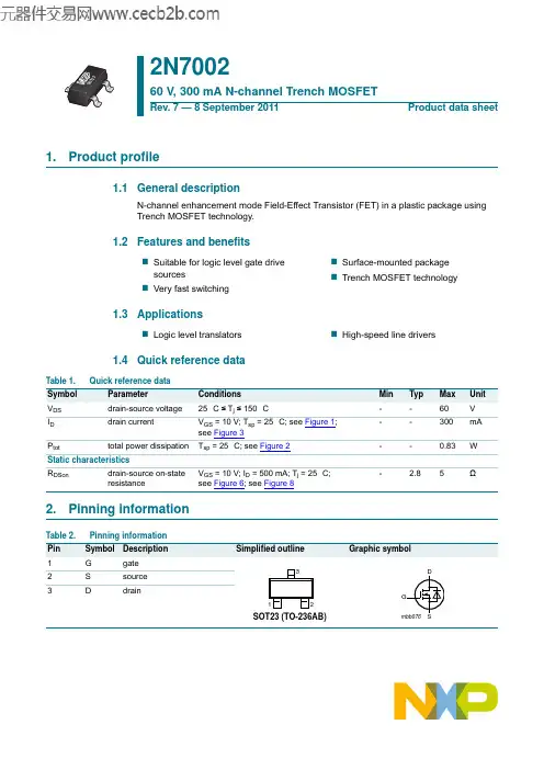
1.Product profile
1.1General description
N-channel enhancement mode Field-Effect Transistor (FET) in a plastic package using Trench MOSFET technology.
1.2Features and benefits
Suitable for logic level gate drive sources
Very fast switchingSurface-mounted package
Trench MOSFET technology
1.3Applications
Logic level translatorsHigh-speed line drivers
1.4Quick reference data
2.Pinning information2N7002
60 V, 300 mA N-channel Trench MOSFET
Rev. 7 — 8 September 2011
Product data sheetSOT23
Table 1.Quick reference dataSymbolParameterConditionsMinTypMaxUnit
VDSdrain-source voltage25°C≤Tj≤150°C--60V
IDdrain currentVGS=10V; Tsp=25°C;seeFigure 1; see Figure 3--300mA
Ptottotal power dissipationTsp=25°C;seeFigure 2--0.83WStatic characteristics
RDSondrain-source on-state resistanceVGS=10V; ID=500mA; Tj=25°C; see Figure 6; see Figure 8-2.85Ω

Prelim. 9/992N7000
Semelab plc.Telephone +44(0)1455 556565. Fax +44(0)1455 552612.E-mail: sales@Website:
N–CHANNELENHANCEMENT MODEMOS TRANSISTORFEATURES• V(BR)DSS= 60V• RDS(ON)= 5W• ID= 1AV
DSDrain – Source VoltageV
GSGate – Source VoltageIDDrain CurrentIDMPulsed Drain Current PDPower Dissipation@ TCASE= 25°CDerate above 25°CTj,TstgOperating and Storage Temperature RangeTLMaximum Lead Temperature for Soldering Purposes, 1/16 from case for 10 seconds60V±40V200mA500mA400mW3.2mW/°C–55 to 150°C300°CMECHANICAL DATADimensions in mm (inches)
ABSOLUTE MAXIMUM RATINGS (TCASE= 25°C unlessotherwise stated)TO92 PACKAGEPIN 1 – DrainPIN 2 – Gate PIN 3 – Drain元器件交易网
THERMAL CHARACTERISTICMin.Typ.Max.UnitRqJAThermal Resistance, Junction to Ambient312.5°C/WV(BR)DSSGate – Source Breakdown VoltageVGS(th)Gate Threshold VoltageIGSSGate – Body Leakage Current ForwardIDSSZero Gate Voltage Drain CurrentID(on)*On–State Drain CurrentRDS(on)*Drain – Source On ResistanceVDS(on)*Drain – Source On VoltagegFS*Forward TransconductanceCissInput CapacitanceCossOutput CapacitanceCrssReverse Transfer CapacitancetONTurn–On TimetOFFTurn–Off Time

MSC1056.PDF 05-19-99
2N3584ABSOLUTE MAXIMUM RATINGS:SYMBOLCHARACTERISTICVALUEUNITSVCBO*Collector-Base Voltage375VoltsVCEO*Collector-Emitter Voltage250VoltsVCER*Collector-Emitter Voltage RBE = 50Ω300VoltsVEBO*Emitter-Base Voltage6VoltsIC*Peak Collector Current5AmpsIC*Continuous Collector Current2AmpsIB*Base Current1AmpsTSTG*
Storage Temperature-65 to 200°CTJ*Operating Junction Temperature-65 to 200°C*Lead Temperature 1/16" from Case for 10 Sec.235°
CPT*
θ JCPower DissipationTC = 25°CThermal Impedance355.0Watts°C/W5 Amp, 375V,High VoltageNPN Silicon PowerTransistors
TO-66APPLICATIONS:
• Off-Line Inverters• Deflection Circuits• Switching Regulators• DC-DC Converters• Motor Controls• High Voltage Amplifiers7516 Central Industrial DriveRiviera Beach, Florida33404PHONE: (561) 842-0305FAX: (561) 845-7813
DESCRIPTION:These power transistors are produced by PPC's DOUBLEDIFFUSED PLANAR process. This technology produces highvoltage devices with excellent switching speeds, frequencyresponse, gain linearity, saturation voltages, high current gain,and safe operating areas. They are intended for use inCommercial, Industrial, and Military power switching, amplifier,and regulator applications.

2N58842N5886
COMPLEMENTARY SILICON
HIGH POWER TRANSISTORS
sSGS-THOMSON PREFERRED SALESTYPES
sCOMPLEMENTARY PNP - NPN DEVICES
sHIGH CURRENT CAPABILITY
APPLICATIONS
sGENERAL PURPOSE SWITCHING ANDAMPLIFIER
sLINEAR AND SWITCHING INDUSTRIALEQUIPMENT
DESCRIPTION
The 2N5884 and 2N5886 are complementary
silicon power transistor in Jedec TO-3 metal case
inteded for use in power linear amplifiers and
switching applications.INTERNAL SCHEMATIC DIAGRAM
June 1997 12
TO-3
ABSOLUTE MAXIMUM RATINGS
SymbolParameterValueUnit
PNP2N5884
NPN2N5886
VCBOCollector-Base Voltage (IE = 0)80V
VCEOCollector-Emitter Voltage (IB = 0)80V
VEBOEmitter-Base Voltage (IC = 0)5V
ICCollector Current25A
ICMCollector Peak Current50A
IBBase Current7.5A
PtotTotal Dissipation at Tc ≤ 25 oC200W
TstgStorage Temperature-65 to 200oC
TjMax. Operating Junction Temperature200oC