STM32 NUCLEO板用户手册
- 格式:pdf
- 大小:1.47 MB
- 文档页数:49
User ManualRIVERDI STM32 Evaluation BoardRev. 1.4 2021-06-02R i v e r d i E v a l u a t i o n B o a r d U s e r M a n u a lREVISION RECORDREVNO. REVDATE CONTENTS REMARKS1.0 2020-08-17 Initial Release1.1 2020-11-06 CPU information updated1.2 2021-03-09 Pictures updated1.3 2021-03-31 Document adjusted into standard template1.4 2021-06-02 Corrections on description related to jumper P7,P8,P9CONTENTSREVISION RECORD (2)Target readers (4)Overview (4)Introduction (5)Board functionality test (5)Interfacing with EVE Displays (6)Using the SPI on the STM32 (10)Hardware features (11)7.2.1 Internal (11)7.2.2 External (12)Additional literature (14)Warranty limitation (14)Legal information (14)Appendix (15)Target readersThe aim of this document is to enable engineers using Riverdi STM32 Evaluation Board to get the tested Riverdi display running fast and easily. Further tests and development can be carried out shortly after Riverdi STM32 Evaluation Board is switched on for the first time.OverviewThe Riverdi evaluation board is designed as a complete demonstration and development platform for Riverdi’s EVE and IPS displays lines driver technology.The Riverdi evaluation board features an STM32F469II Cortex-M4 microcontroller with: LCD parallel interface including 8080/6800 modes, an LCD-TFT controller, Chrom-ART Accelerator™ for enhanced graphic content creation (DMA2D), secure digital input/output interface (SDIO), LTDC signals available on header P11 with additional MCU pins broken out on P12, external SDRAM, MicroSD slot for data/media storage, RiBUS FFC conn P3 featuring SPI, UART and LCD supply pins (SPI can be controlled by either STM32 or UBS serial bridge via jumper on P7/8/9) and configurable display backlight supply (EXT/INT).IntroductionRiverdi STM32 Evaluation Board is a tool designed to help get you started on working with Riverdi products. It not only supports EVE modules but also RGB displays (in combination with touch panels) by Riverdi.You have two primary options to drive external displays:1.Jumper between P7 & P8: FTDI serial/SPI bridge connected to RiBUS SPI:Use the FT232 serial to SPI bridge by connecting a micro USB cable to the connector labeled “Direct USB” and using the EVE Screen Editor to quickly generate graphical user interfaces with minimum effort .2.Jumper between P9 & P8: STM32 connected to RiBUS SPI:Use the onboard STM32F4 to develop and test firmware for driving a connected display or display controller, like the FT80x, FT81x and BT81x series.Board functionality testThere are firmware examples with which you can test your Riverdi STM32 Evaluation Board. You can also use those as a starting point for your own firmware development.Interfacing with EVE DisplaysUsing the FTDI SPI Bridge & EVE Screen EditorPrerequisites:•Riverdi STM32 Evaluation Board•EVE-enabled display•RiBUS flexible flat cable (FFC)EVE Screen Editor InstallationDownload and install the EVE screen Editor from the FTDI homepage:https:///Support/Utilities.htm#EVEScreenEditorSetup & ConfigurationTo connect the FTDI SPI bridge to the EVE display, the configuration jumpers need to be placed between P7 and P8, as in the picture below.Set the backlight jumper (placed over the backlight power configuration pins) to 5V BL on P4 (also refer to the picture below). Please see description on how to connect power for backlight in section “Hardware features”, subsection “Backlight power supply”.Start EVE Screen Editor and you will be greeted with the screen similar to the one below:On the lower right hand side of the window, click on the ”Devices” tab.On the lower left hand side, you will find 3 buttons:This button refreshes the devices list above it;This button opens a menu to select one from the preconfigured displays list;This button opens a menu to define your own display to be driven.Use a USB cable to connect the “USB Direct” port to your computer, when running the EVE Screen E ditor application. Click the “Refresh” button afterwards and your dev board should show up like in the picture below:Select "Single RS232-HS ()” entry by clicking on it and use the ‘Connect’ button to let EVE Screen Editor try and boot up your display.If everything works properly, your display should show a blue screen with some text.Hello WorldAfter connecting to Eval Board, to generate its first text message (e. g. 'Hello World'), we are going to use the EVE Screen Editor’s built-in drag & drop editor.(The drag operation is shown in green, the generated coprocessor commands are shown in the yellow box and the button to send the data to the EVE display is seen inside the red box.)What you see now is the preview of what will be drawn on the physical screen in a moment. Note that in the lower part of the window the coprocessor tab shows which EVE pre-processor commands were generated and will be sent to the EVE display shortly after.To send the commands also drawn in the preview pan to the physical display, press the button labeled “Upload RAM_G and RAM_DL”.Using the SPI on the STM32Prerequisites•Riverdi STM32 Evaluation Board•EVE enabled display•RiBUS flexible flat cable (FFC)•Your favorite tool to flash the onboard STM32 (assuming that you use STM32CubeProgrammer together with an STLink v2 compatible ISP Programmer)InstallationUse the provided source code or the pre-compiled binary file.ConfigurationIn order to connect the STM32 to the EVE display, the configuration jumpers need to be placed between P9 and P8. Check the jumper and the USB cable position (in ‘STM32 USB’ socket) in the picture below.Hardware featuresModule power supplyPossible to deliver from one of 2 USB ports on Eval Board (“Direct USB” or “STM32 USB”), in accordance with USB standard (5.0 VDC max.)Backlight power supply7.2.1InternalFor display sizes from 3.5” to 5.0”, the USB port gives enough power to get adequate backlight level. Such backlight power supply configuration (jumper is in higher position, connects BL to 5V on P4) is shown in the picture below.For 7.0” displays, USB minimal power capability needs to be 700mA @ 5V (this is a combined power of Eval Board, BT817Q board and backlight). Please make sure your USB source has enough current efficiency. If not, use external 5V power source in the way described in point 6.2.2.7.2.2ExternalAll the 10.1” (and rarely certain 7.0” displays) require external power supply for backlight, as the backlight voltage exceeds 5V and power consumption is over the USB standard. To provide adequate backlight power, set the jumper in P4 to lower position (it connects BL to EXT) – it must be placed in lower position and connect the external DC voltage source to neighboring connector (“BL PWR”). Refer to the picture and below.Caution! There is no reverse polarity protection on EXT_BL_PWR, incorrect connection will damage the backlight permanently. Proceed carefully.EVE4 BT817Q TFT series backlight power requirement summary:Display size Internal (from USB) External3.5”OK 3.3V-6.0V (optional)4.3”OK 3.3V-6.0V (optional)5.0”OK 3.3V-6.0V (optional)7.0”Ok, if USB has 700mA min. efficiency 3.3V-6.0V (optional)You can find exact currents for specific TFT in datasheet:https:///product-category/intelligent-displays/bt817q/MicrocontrollerSTM32F469II, Arm Cortex-M4 MCU @ up to 180MHzExternal SDRAMIS42S16400J, 64Mbit/WW/pdf/42-45S16400J.pdfFTDI serial to SPI bridgehttps:///Support/Documents/DataSheets/ICs/DS_FT232H.pdfMicroSD slotWhen functional microSD card is placed in this slot, after being formatted in FAT32 format, microSD card’s memory space can be used by microcontroller as the regular filesystem.RiBUS FFC-connectorSupport for FT80x, FT81x, BT81x (max SPI speed = 30MHz),https:///download/5318/FTDI app note AN312 contains c headers and example code for FT800User LEDs: 2 pcsThey can be configured by the user, from program level.Power LED indicating power to FTDI "Direct USB”FTDI input powers both rails.Power LED indicating power to STM32 "STM32 USB"STM32 powers its own rail only.User Buttons: 2 pcsThese may be used in future, they are not used now.Serial RGB bus headerPlease refer to Application Note: ST AN4861 (LCD-TFT display controller (LTDC) on STM32 MCUs).Additional literatureAll the below sources contain the data of four BT815/816 (EVE3) and BT817/BT818 (EVE4) ICsBT81x, General:https:///bt81x/BT81x, Datasheets:https:///wp-content/uploads/Support/Documentation/Datasheets/ICs/EVE/DS_BT81X.pdfBT81x, Programming guides:https:///wp-content/uploads/Support/Documentation/Programming_Guides/ICs/EVE/BRT_AN_033_BT81X_Serie s_Programming_Guide.pdfWarranty limitationEnd user is instructed how to connect external power sources to the unit, which brings the potential threats to the Eval Board and display. Riverdi cannot be held responsible for actions beyond its control and consequently the warranty DOES NOT cover the effects of reversed power supply polarity on backlight terminals. Refer to clause in red color in section 6.2.2 of this documentLegal informationThis document has been issued with professional care. Riverdi did their best to avoid any errors, but we do not grant full warrant it is 100% errors free. Please contact Riverdi if you find any mistakes or when you think some important information is missing in this Manual.It can be updated or altered without any written notice. Riverdi cannot be held responsible for not announcing any changes or issuing next revisions or versions of this document.AppendixHardware Pinouts# Pin Description MCU Peripheral25 PF7 User Led 1 (left) GPIO Output26 PF8 User Led 2 (right) GPIO Output53 PA7 User Button 1 GPIO Input (enable pull-up)50 PA4 User Button 2 GPIO Input (enable pull-up) 130 PH15 uSD Detect (hi: uSD present) GPIO Input (enable pull-up)40 PA0 STL_TX (UART) UART4 TX41 PA1 STL_RX (UART) UART4 RX95 PB15 R_MOSI (SPI2) SPI2 MOSI94 PB14 R_MISO SPI2 MISO93 PB13 R_CLK SPI2 SCK92 PB12 R_CS SPI2 NSS86 PH9 R_INT GPIO Input84 PH10 R_RST GPIO Output5 MOSI / IO.0 PI MISO Signal / QSPI data line 06 CS SPI Chip Select Signal7 INT Interrupt Signal (Out to MCU)8 RST / PD Reset / Power Down Signal9 - 14 NC NC15 RX UART RX / I2C16 TX UART TX / I2C17 BLVDD Backlight Power Supply, 5V18 BLVDD Backlight Power Supply, 5V19 BLGND Backlight Ground (GND on display)20 BLGND Backlight Ground (GND on display)GND 1 2 3.3V VCCMOSI 3 4 SCKnCS 5 6 MISOnRST 7 8 nINTNC 9 10 NCNC 11 12 NCNC 13 14 NCTX 15 16 RX5V Backlight 17 18 5V BacklightGND 19 20 GND。
STM32 LL库使用指南---By Fengzi熟悉STM32的都知道ST官方提供了非常方便好用的库函数供用户使用,多数人都使用过STM32标准外设库,STM32Cube库(即HAL库),这个LL库是什么鬼,却从来没听说过。
好吧,我承认这个名字是我自己XJB取的。
目录一、初识LL 库 (1)二、怎么使用LL库 (3)三、新建STM32LL库工程模板 (5)四、第一个程序——点亮LED (8)五、添加其他程序功能 (10)………………………………………………………………………………………………………………………………………………….一、初识LL 库最近论坛发的STM32L476RG Nucleo开发板到手了,准备学习玩耍,当然第一步就是下载资料,于是我下载STM32L4Cube 1.1.0版本,打开逐个查看,好像和以前一样的,没什么特别嘛,于是准备开始开发。
等等,好像还真发现了有点不一样:熟悉HAL库的都知道,该库的文件几乎都是以stm32xxx_hal_xxx.h/.c命名的,为了和以前的标准库有个区分,上图中那些是什么鬼前辈说,遇到问题赶紧查手册,于是我果断打开STM32L4Cube库的说明手册(UM1884):原来这个东西叫做Low Layer APIs,作为英文渣渣表示实在不习惯洋里洋气的高大上名字,于是擅自把他叫做【STM32LL库】了(不服的你咬我啊)。
从这里看好像是说这个东东比HAL库更接近硬件,到底什么鬼,还不清楚。
但是以前好像没见过这个东西啊,就算是STM32L4Cube的1.0.0版本中都没有。
看看Cube发行历史:原来LL库是在1.1.0版本才加上的,大概意思就是:1.LL APIs是寄存器级的编程,嗯,也就是说我们常说的直接操作寄存器吧。
2.LL APIs适用于xxx等一大堆外设3.LL APIs函数全部定义为static inline函数,放在对应的头文件中,用户使用需要包含相关头文件4.参考这两个文档看看LL库文件在Cube库中的位置,有20多个文件,全部以stm32l4xx_ll_xxx.h命名:STM32Cube_FW_L4_V1.1.0\Drivers\STM32L4xx_HAL_Driver\IncSTM32L4是面向低功耗市场的,同时不失高性能,功耗和性能往往是两个矛盾的东西,ST在硬件设计上想了各种办法来实现兼顾低功耗高性能(例如各种低功耗模式,LP外设等),而在软件层面,程序也讲求效率,LL库全是直接操作寄存器,直接操作寄存器往往效率较高,而且函数定义为内联函数,调用函数时不是堆栈调用,而是直接把函数的代码嵌入到调用的地方,利于提高代码相率,我想这也是ST在STM32L4系列中推出这个直接操作寄存器的LL库的原因之一吧。
XNUCLEO USER MANUAL●Compatible with NUCLEO serials.●Arduino connectivity support, easy to connect with various Arduino shields and access themassive Arduino resources●ST Morpho headers provide full access to all STM32 I/Os, easy for peripheral expansion●Supports mbed, build prototype quickly by mbed SDK and online tools●Comprehensive free software HAL library including a variety of software examples●Comes with a separated ST-LINK/V2 module1ORDERING INFORMATIONTable 1: Xnucleo series product informationThe meaning of XNUCLEO-FXXXRY codification is as follows:●FXXX describes the STM32 MCU product line;●R describes the pin count (R for 64 pins);●Y describes the FLASH size (8 for 64K, B for 128K, C for 256K).2Features (1)Advantages (1)Ordering Information (2)1.Quick Start (5)1.1.Development tool installation (5)1.1.1.CP2102 Virtual COM Port driver installation (5)1.1.2.STM32 ST-LINK Utility installation (5)1.1.3.J-Link driver installation (5)1.2.Getting started (5)1.2.1.Hardware configurations (6)1.2.2.Observing the actions (6)2.Hardware configuration (7)2.1Power supply settings (7)2.1.1Power supply input from the USB connector (7)2.1.2Using CN2, VIN or E5V as external power supply (8)2.1.3External power supply output (9)2.2LED indicators (9)2.2.1FLASH LED (9)2.2.2PWR LED Power supply indicator (9)2.2.3Serial port working status LED indicators (10)2.3Push button (10)2.3.1USER button (10)2.3.2RESET button (10)2.4JP2 (IDD) jumper settings (10)2.4.1JP2 ON (10)32.4.2JP2 OFF (10)2.5USART communication (10)2.5.1Connecting the targeted MCU to serial port (10)2.5.2Communication between the targeted MCU and shield or extension board (11)2.6ADC or I2C communication (12)2.7SPI connector (12)2.8USB connector (13)2.9Solder bridges (13)2.10Extension connector (13)3.How to use mbed on STM32 Xnucleo platform (16)3.1How to compile and download program under mbed (16)3.1.1Program compiling (16)3.1.2Program downloading (16)3.2How to export the Keil program from mbed (17)4.Periphery module Demo (18)4.1Connection between the Xnucleo board and Peripherals (18)4.2Demo explanations (20)4.2.1Data display mode (20)4.2.2The meanings of the returned data (21)41.1.1.DEVELOPMENT TOOL INSTALLATIONSTM32 Xnucleo includes an onboard USB TO UART interface based on CP2102 (“serial port”hereafter) for code debugging. Before using this interface, you should install a CP2102 driverfirstly.Run the installer: .\Xnucleo \tools\CP2102 driver\PreInstaller.exeWhen the installation finished, connect the XNucleo board to a PC via the USB TO UART interface.And you will find the CP210x USB to UART Bridge Controller in the Device Manager, if the driver is installed successfully.Run the installer: .\Xnucleo user\tools\STM32 ST-LINK Utility\STM32 ST-LINK Utility_v3.4.0.exe (For more detailed information about installation and usage of STM32 ST-LINK Utility, pleaserefer to the document provided by ST: .\Xnucleo user\tools\STM32 ST-LINKUtility\Readme\STLINK Utility.PDF. You can also download the latest installer from the STwebsite).When the installation finished, connect the ST-LINK/V2(mini) module to a PC. You will find the STMicroelectronics STLink dongle in the Device Manager, if the driver is installed successfully.Run the installer:.\Xnucleo user\tools\JLinkARM\Setup_JLinkARM_V415e.exeWhen the installation finished, connect the J-Link emulator to a PC. You will find the J-Link driver in the Device Manager, if the driver is installed successfully.1.2.GETTING STARTEDPlease follow the sequence below to configure the STM32 Xnucleo board and launch the demo software:561) Jumper settings ● Set JP3 to U5V; ● Set JP2 to ON;2) Power supply and power selection●For using a USB power supply, connect the Xnucleo board to a PC with a USB cable through the onboard USB connector; ●For using an external power supply, connect the power supply socket CN2 on the Xnucleo board to a 6~12V power adapter. 3) Connect the ST-LINK/V2 (mini) debugger/programmer to the SWD connectorNotices: It is recommended to plug in the USB power supply or the external power supply before connecting the ST-LINK/V2(mini) module to the SWD interface. Otherwise, the ST-LINK/V2(mini) initialization may be failure.The blinking of the USER LED indicator will change from fast to slow or from slow to fast, when clicking the USER key.2.2.1POWER SUPPLY SETTINGSThe power supply of the STM32 Xnucleo board is provided either by the host PC through the USB cable, or by an external source:●VIN (7V~12V) or +3V3 power pins on CN6;●E5V(5V) pin on CN7;●CN2 power supply connector (7V~12V).In case VIN, E5V, +3V3 or CN2 is used to power the Xnucleo board, you should use an external power supply unit.All parts of the STM32 Xnucleo board and Shield can be powered from the ST-LINK/V2 (mini) USB connector by the host PC.In case the ST-LINK/V2 (mini) USB connector is used to power the Xnucleo board, the host PC will provide 150mA current at maximum as 3.3V voltage is outputted from the ST-LINK/V2 (mini) USB connector to the Xnucleo board. And 300mA current at maximum may be provided when 5V voltage is outputted to the Xnucleo board. In case of the board requiring the current more than 300mA, it should be mandatory to use an external power supply as explained in the next chapter.Each part of STM32 Xnucleo including the extension board can be powered by USB(U5V).However, if the maximum current consumption of the board exceeds 300mA, the USB may be damaged. When the board is power supplied by USB(U5V), a jumper must be connectedbetween pin 1 and pin 2 of JP5 as shown in Table 2.Table 2: Power-related jumper7U5V (ST-LINK VBUS) is used as power source when JP5 is set as shown below (Defaultsetting)CN2, VIN or E5V is used as power source when JP5 is set as shown belowCN2, VIN or E5V can be used as external power supply in case the current consumption of Xnucleo and its extension boards exceeds the allowed current on USB. In this condition, it is mandatory to power supply the board using the external power source firstly, then connect the USB cable and ST-LINK/V2 (mini) to the PC to ensure that the Xnucleo board can work properly.Table 3: External power source parametersNotices: The following power sequence procedure must be respected when using an external power source:1)Set JP3 to U5V;2)Connect the external power source to CN2, VIN or E5V;3)Power on the external power supply CN2, VIN: 7V~12V, or E5V: 5V;4)Check that PWR LED is turned ON;5)Connect the PC to USB connector or ST-LINK/V2(mini) on Xnucleo.89If this order is not respected, the board may be supplied by VBUS or ST-LINK/V2(mini) firstly, and the following risks may be encountered:If more than 300 mA current is needed by the board, the PC may be damaged or the current supply can be limited by the PC. As a consequence the board cannot work correctly.●When powered by CN2, VIN or E5V, the +5V (CN6 pin 5 or CN7 pin 18) can be used as output power supply for an Arduino shield or an extension board. In this case, the maximum current of the power source specified in Table 3 needs to be respected. ●The +3.3 V (CN6 pin 4 or CN7 pin 12 & 16) can be used also as power supply output. The current is limited by the maximum current capability of the regulator U4 (500 mA max).2.2LED INDICATORSThe LEDs on the STM32 Xnucleo board is used to provide information about the Xnucleo working status.Table 4: The relationship between LED and the pins of MCUIt is easy to use each LED by setting JP7. For XNUCLEO-F302R8, the pin PB13 is connected to the MCU pin D13. And for other XNUCLEO devices, the pin PA5 is connected to the MCU pin D13. When the I/O is HIGH value, the FLASH LED is on. And when the I/O is LOW, the FLASH LED is off.10The PWR LED default color is red. It indicates the power supply status of the STM32 Xnucleo board. The red LED indicates that the MCU part is powered by +5V.TX indicator is in green, and RX indicator in blue. The blinking TX indicator means the MCU of STM32 Xnucleo board is sending message to the targeted PC. The blinking RX indicator means the MCU of STM32 Xnucleo board is receiving message from the targeted PC.2.3PUSH BUTTON The USER button is connected to the I/O PC13(pin 2) of the targeted MCU by setting JP6 to ON;This RESET button is connected to NRST, and is used to reset the targeted MCU.2.4JP2 (IDD) JUMPER SETTINGS STM32 microcontroller is powered (default).When this jumper is removed, STM32 microcontroller is not powered. But you can connect an ammeter on the JP6 to measure the STM32 microcontroller current.2.5USART COMMUNICATIONThe USART2 interface available on PA2 and PA3 of the STM32 microcontroller can be connected to Virtual COM Port, STMicroelectronics Morpho connector or to Arduino connector.Please set the JP4 as follows, to connect the targeted MCU to serial port (For more information, please refer to Table 6 and Table 7).●Connect the RX/PA3 of JP4 to the TXD;●Connect the TX/PA2 of JP4 to the RXD.If the communication between the targeted MCU and shield or extension board is required, you should set the JP4 and the RX/D0 and TX/D1 on CN9 as follow (For more information, please refer to Table 6).●Connect the RX/PA3 of JP4 to the RX/D0;●Connect the TX/PA3 of JP4 to the TX/D1.In such case it possible to connect another USART (if another USART is available on the targeted MCU) to the targeted MCU through Virtual COM Port using flying wires as follow●Connect the TX/PC10/PC6 of JP4 to RXD;●Connect the RX/PC11/PC of JP4 to TXD.Here is the jumper setting for connecting to XNUCLEO-F030R8:●Connect the TX/PA9 of JP4 to RXD;●Connect the RX/PA10 of JP4 to TXD.Notices: You should select a proper USART by referring to Table 5 and make corresponding hardware configurations, according to your actual demand. The USARTs (USART1 and USART3) listed in this table are unavailable under mbed, since only USART2(PA2, PA3) is defined for mbed. Therefore, when the USART-related APIs (such as printf) are required under mbed, you should select USART2(PA2, PA3) to connect to Virtual COM Port or CN9 on the pins RX/D0 and TX/D1.Table 5: USART-related pins and jumpers1112Table 6: Connections of JP4 pinsTable 7: Connections of NUCLEO-F030R8 JP42.6ADC OR I2C COMMUNICATIONIf ADC or I2C communication is required, you can connect the ADC interface or the I2C interface to the Arduino connector or the ST Morpho connector by setting the JP5. Here are the relative settings to JP5:●The pins A4 and A5 of JP5 should be connected to the Arduino connector on the pins A4 and A5 (the pin 5 and the pin 6 of CN8) or the ST Morpho connector on the pins 36 and 38 of CN7 respectively; ● The pins SDA/PB9 and SCL/PB8 of JP5 corresponding to the I2C interface of STM32 MCU; ●The pins PC1/ADC and PC0/ADC of JP5 corresponding to the ADC interface of STM32 MCU.Table 8: Connections of JP5 pins2.7 SPI CONNECTORThe pins D11, D12 and D13 of Arduino connector are SPI interfaces. For XNUCLEO-F302R8, the pins PB13, PB14 and PB15 are connected to the pins D13, D12 and D11, respectively. And for other XNUCLEO devices, the pins PA5, PA6 and PA7 are connected to the pins D13, D12, and D11, respectively.2.8USB CONNECTORExcept the XNUCLEO-F030R8, all the other XNUCLEO devices have reserved a USB connectorwhich can be enabled by setting JP1 to ON.2.9SOLDER BRIDGESTable 9: solder bridgesNotes: All the other solder bridges present on the STM32 Xnucleo board are used to configure several IOs and power supply pins for compatibility of features and leads with STM32 MCU supported.2.10EXTENSION CONNECTORThe following figures show the signals connected by default to Arduino connectors (CN5, CN6, CN8, CN9) and to ST Morpho connector (CN7 and CN10), for each STM32 Xnucleo board.13Figure 1: XNUCLEO-F030R8Figure 2: XNUCLEO-F103RBFigure 3: XNUCLEO-F302RC14Figure 4: XNUCLEO-F401REFigure 5: XNUCLEO-F411RE153.Xnucleo series is fully compatible with Nucleo series and can run the Nucleo Demos directly.Therefore, you can develop your STM32 Xnucleo applications based on the applications ofSTM32 Nucleo. Table 10 gives the relationship between Xnucleo series and Nucleo series.Table 10: Relationships between Xnucleo series and Nucleo seriesThe operations presented in this document are based on XNUCLEO-F103RB. For differentXnucleo devices, there may be some differences in configuring the development environment.So users should operate according to the actual conditions.3.1HOW TO COMPILE AND DOWNLOAD PROGRAM UNDER MBEDIn this section, we only present the ways to compile and download program, since it does not have room to address every factor of mbed. For more detailed information about the usage of mbed, please refer to the documents provided by mbed organization.Here we take XNUCLEO-F103RB as an example. Start the mbed software, and open a program,no error, Compile Output will show “Success!” after the compiling is finished. And the fileNucleo_printf_NUCLEO_F103RB.bin will be generated. This file can be found in the specified save path (This save path is modifiable).1)Run the STM32 ST-LINK Utility, and select file->Open file. Then, open the fileNucleo_printf_NUCLEO_F103RB.bin.162)Connect the USB TO UART interface on the board to your PC with a USB cable, and thenconnect ST-LINK/V2(mini) module to download the .bin file. Then, set the JP5 to U5V. Forthe JP4 setting, please refer to Section 2.5 USART communication. The serial port should beconfigured according to Table 11.Table 11: Serial port configurationBaud rate 115200Data bit 8Stop bit 1Parity None3)When the program downloading finished, COM port will receive the following information:Hello World!This program runs since 1 second.This program runs since 2 seconds.This program runs since 3 seconds.This program runs since 4 seconds.This program runs since 5 seconds....At this time, the USER LED is blinking in the frequency of 0.5Hz. And the TX LED keepsblinking to indicate that STM32 Xnucleo is sending message to the PC.3.2HOW TO EXPORT THE KEIL PROGRAM FROM MBEDCircuit debugging are unavailable in mbed. However, mbed has “Import Program” and “Export Program” functions. You can export the programs in mbed as Keil programs to performdebugging.The mbed library file can also be exported, which includes the HAL library of STM32 MCU. Under the Keli environment, mbed libraries can be applied or modified directly, and can betransplanted into other applications.17The relative operations are as follow:In the mbed, open the program you want to export. Then, right click the program name in the Program Workspace, and select Nucleo_printf->Export Program, as Figure 6 shows.Figure 6: Exporting as Keil programIn the Export Toolchain pull-down menu of the pop-up window, select Keil μVision. Then, the programs in mbed can be exported as Keil programs and performed Keil debugging. For more detailed information, please refer to the Keil-related technical documents.4.PERIPHERY MODULE DEMOBesides Nucleo Demos, the Demos for different periphery modules provided by Waveshare are supported by Xnucleo series as well. The corresponding devices to the periphery module Demos include but not limited to: Temperature-Humidity Sensor, Rotation Sensor, Color Sensor, UV Sensor, Water Sensor, Moisture Sensor, Vibrating Sensor, Tilt Sensor, Laser Sensor, Gas Sensor, Sound Sensor, Flame Sensor, Hall Sensor, Metal Sensor, Infrared Reflective Sensor, OLED display module and so on. And these Demos for different periphery modules are integrated into a big Demo (“periphery module Demo” hereafter) for convenience.4.1CONNECTION BETWEEN THE XNUCLEO BOARD AND PERIPHERALSTable 12: Connection between the XNUCLEO and sensors1819Notices:●The pins VCC and GND of the sensors listed above should be connected to the pins VCC andGND of IO Expansion Shied. For more detailed information, please refer to IO ExpansionShied User Manual.●Some of the sensors may only lead out the pin AOUT or the pin DOUT. In this case, theadditional reserved pin(s) of IO Expansion Shied can be left unconnected. One IO ExpansionShied can only connect one sensor at a time.4.2DEMO EXPLANATIONSWhen the Demo is running, the LED1 on the XNUCLEO board will blink at the rate of every 2seconds.For the periphery module Demo, there are two modes for displaying the returned information from the module: OLED and Screen Print (relative information is sent to the PC via the serial port every 500 ms). Here is an example:Figure 7: OLED displays relative sensor parameters2021At the same time, relative data will be outputted:/*----------------------*/T: 23 C H: 34D: 3868 A: 3.116 S: OFFRot: 227 SW: 52R: 20G: 6 B: 105RTC: 12:1:4 KEY: 10/*----------------------*/Table 13: The meanings of relative symbols22。

STM32 Nucleo扩展板STM32 ODE快速、经济的原型设计和开发STM32开放开发环境(ODE)在一个开放、灵活、简单、经济的开发环境下,基于STM32位微控制器,结合其他通过扩展板连接的ST尖端原件,从而快速进行原型设计,迅速转换为最终设计。
STM32 ODE包括下述五个单元:• STM32 N ucleo开发板。
全面的经济型开发板,适用于所有STM32微控制器系列,具有无限的统一扩展能力,具有集成的调试器/编程器。
• STM32 N ucleo扩展板。
该扩展板具有更多功能,能按需增加传感、控制、连接、供电、音频或其他功能,可以插在STM32 Nucleo开发板上,更复杂的功能可以通过堆叠更多的扩展板来实现。
• STM32Cube软件。
协助迅捷地在STM32上开发的一套免费工具和嵌入式软件模块,包括硬件抽象层、中间件和STM32CubeMX 基于PC的配置器和代码生成器。
• STM32Cube扩展软件。
该扩展软件免费提供,与STM32 Nucleo扩展板配置使用,兼容STM32Cube软件框架。
• STM32Cube功能包。
功能案例集合包含一些最常见的应用样例,这些案例均利用STM32 N ucleo开发板和扩展板、STM32Cube软件和扩展的模块化和互操作性构建。
STM32开放式开发环境兼容许多IDE(包括STM32CubeIDE、IAR EWARM、Keil MDK-ARM和GCC/基于LLVM的IDE),能够集成各种组件,如STM32CubeMX、STM32CubeProgrammer或STM32CubeMonitor。
详情请访问/stm32ode23众多可扩展板的组合不仅基于先进商用产品,而且提供了模块化软件,从驱动器到应用层,可实现方案的快速成型,顺利转化为最终设计。
如需开始您的设计:• 选择符合您所需功能的合适STM32 N ucleo 开发板(MCU )和扩展(X-NUCLEO )板(传感器、连接、音频、电机控制等)• 选择您的开发环境(IAR EWARM 、Keil MDK 和基于GCC 的IDE ),并使用免费的STM32Cube 工具和软件,如STM32CubeMX 、STM32CubeProgrammer 、STM32CubeMonitor 或STM32CubeIDE 。

STM32F103VET6芯达 STM32○RUser's ManualPreliminaryRevision 1.0(2010.06.08) 芯达STM32开发板开发指南Copyright © 2009‐2010 ARM79 Limited. All rights reserved版本信息本手册进行了以下更改。
芯达STM32用户手册修订记录日期 修订版本 CR ID 修改章节 修改描述 作者 2010-5-28 1.00 全部 创建 林辰 2010-8-16 1.10 去掉蜂鸣器、AT45 林辰 2010-8-20 1.20 增加外扩接口、修林辰改外观图片版权声明本手册版权归属(以下简称“arm79”)所有, 并保留一切权力。
非经arm79同意(书面形式),任何单位或个人不得擅自摘录本手册部分或全部,违者我们将追究其法律责任。
敬告:在售开发板的手册会经常更新,请在网站查看最近更新,并下载最新手册,不再另行通知。
目录目录 (4)写在前面 (5)第一章芯达STM32光盘使用说明 (6)第二章芯达STM32硬件说明 (8)2.1 芯达STM32板载资源说明 (8)2.2 芯达STM32原理图说明 (9)2.2.1电源电路 (9)2.2.2 实时时钟(备用电池)电路 (9)2.2.3 系统时钟电路 (9)2.2.4 JTAG接口电路 (10)2.2.5 复位电路 (10)2.2.6 用户LED电路 (10)2.2.7 串口电路 (11)2.2.8 按键电路 (11)2.2.9 SD卡接口电路 (12)2.2.10 USB接口电路 (12)2.2.11 LCD TFT液晶接口电路 (13)2.2.12 外扩IO接口电路 (13)第三章芯达STM32开发前的准备 (15)3.1 J-Link驱动的安装 (15)3.2 使用J-Link下载调试 (18)3.3使用ISP下载调试 (25)3.3.1 安装Flash loader (25)3.3.2 使用ISP下载调试 (28)3.4安装RealView MDK软件 (34)3.5使用MDK + J-Link调试 (38)第四章芯达STM32初步开发举例 (49)4.1 下载固件库 (49)4.2 STM32简单开发 (50)附福州芯达工作室简介 (54)写在前面感谢您选购芯达STM32开发板产品!请详细阅读以下文字,以获取对芯达STM32开发板的更多信息。
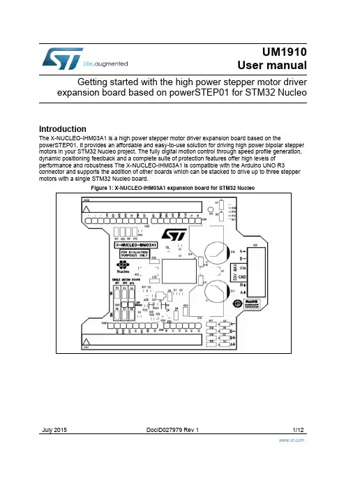
July 2015 DocID027979 Rev 1 1/12UM1910 User manualGetting started with the high power stepper motor driver expansion board based on powerSTEP01 for STM32 NucleoIntroductionThe X-NUCLEO-IHM03A1 is a high power stepper motor driver expansion board based on thepowerSTEP01. It provides an affordable and easy-to-use solution for driving high power bipolar stepper motors in your STM32 Nucleo project. The fully digital motion control through speed profile generation, dynamic positioning feedback and a complete suite of protection features offer high levels of performance and robustness The X-NUCLEO-IHM03A1 is compatible with the Arduino UNO R3connector and supports the addition of other boards which can be stacked to drive up to three stepper motors with a single STM32 Nucleo board.Figure 1: X-NUCLEO-IHM03A1 expansion board for STM32 NucleoContents UM1910 Contents1Getting started (3)2Hardware description and configuration (4)2.1Selecting the chip select and clock lines of the SPI (6)2.2Multi-motor configuration (6)3Revision history (11)UM1910Getting started1 Getting startedThe X-NUCLEO-IHM03A1 expansion board is a high power stepper motor driver covering a wide range of applications. In particular, the maximum ratings of the board are the following. ∙ Power stage supply voltage (VS) from 10.5 V to 50 V ∙ Motor phase current up to 10 A r.m.s.Follow this sequence to start your project with the board:1. Check the jumper position based on your configuration (see Section 2: "Hardware description and configuration").2. Plug the board to the STM32 Nucleo board through Arduino UNO R3 for the X-NUCLEO-IHM03A1.3. Supply the board through the input 1 (VS) and 2 (ground) of the connector CN1. The power OK (green) and fault (red) LEDs will turn on.4.Develop your application using the examples provided with the firmware library, X-CUBE-SPN3, high power stepper motor driver software expansion for STM32Cube. Further support material is available on the powerSTEP01 (/powerstep) and STM32 Nucleo web pages (/stm32nucleo).Up to three expansion boards can be stacked on the same STM32 Nucleo board as described in Section 2.2: "Multi-motor configuration".2 Hardware description and configurationFigure 2: "Jumper and connector positions" shows the position of the connectors and theconfiguration jumpers of the board.Figure 2: Jumper and connector positionsBelow are the pinout details for the Arduino UNO R3 and the ST Morpho connectors.Notes:(1)All the unlisted pins are not connected.Notes:(1)All the unlisted pins are not connected.2.1 Selecting the chip select and clock lines of the SPIThe chip select and the clock lines of the SPI interface can be selected via the appropriateresistors indicated in Table 3: "Chip select line selection" and Table 4: "Clock lineselection".2.2 Multi-motor configurationThe expansion boards can be stacked on a single STM32 Nucleo board in order to drive upto the three stepper motors (one expansion board for each motor is required).The configuration is changed by mounting the resistors from R3 to R8 as listed in Table 5:"Multi-motor setup table".The other resistors are not mounted.By default, the stepper driver board is configured for a single-motor setup, so the boardconfiguration must be changed in multi-motor setups before stacking the boards on theSTM32 Nucleo.UM1910 Revision history 3 Revision historyUM1910IMPORTANT NOTICE – PLEASE READ CAREFULLYSTMicroelectronics NV and its subsidiaries (“ST”) reserve the right to make changes, corrections, enhancements, modifications, and improvements to ST products and/or to this document at any time without notice. Purchasers should obtain the latest relevant information on ST products before placing orders. ST products are sold pursuant to ST’s terms and conditions of sale in place at the time of or der acknowledgement.Purchasers are solely responsible for the choice, selection, and use of ST products and ST assumes no liability for application assistance or the design of Purchasers’ products.No license, express or implied, to any intellectual property right is granted by ST herein.Resale of ST products with provisions different from the information set forth herein shall void any warranty granted by ST for such product.ST and the ST logo are trademarks of ST. All other product or service names are the property of their respective owners.Information in this document supersedes and replaces information previously supplied in any prior versions of this document.© 2015 STMicroelectronics – All rights reserved。
STM32开发板使用说明1、开发板使用到的软件及安装说明在开始学习开发板之前需要安装的软件有:1、KEIL3.80A,2、PL-2303HX驱动,3、串口调试助手,4、下载器MCUISP。
这些软件在课件文件下面的软件文件里。
具体安装步骤如下:1.KEIL3.80A的安装,打开路径:课件\软件\KEIL3.80A\MDK3.80A安装手册,根据上面的步骤安装软件。
2.PL-2303HX驱动的安装,打开路径:课件\软件\PL-2303HX新版驱动,可根据使用电脑的操作系统来选择安装的软件,如选择安装XP驱动,可打开XP驱动,根据里面的安装说明来安装软件。
一般只要运行PL-2303 Driver Installer。
exe就可以了。
3.串口调试助手的安装,打开路径:课件\软件\串口调试助手,点击sscom33。
exe即可,也可以创建快捷方式在桌面。
4.下载器MCUISP的安装,打开路径:课件\软件\下载器MCUISP,点击mcuisp。
exe 即可,也可以创建快捷方式在桌面。
2、开发环境介绍及使用说明首先是我们之前安装的keil3.80a。
再点击Project->New uVision Project如下图所示:弹出create new project 对话框,新建一个文件夹TEST,然后把工程名字设为test。
点击保存。
弹出选择器件的对话框,因为我们的开发板使用的是STM32F103RBT6 ,所以在这里我们选择STMicroelectronics 下面的STM32F103RB( 如果使用的是其他系列的芯片,选择相应的型号就可以了)。
如下图所示:点击OK,MDK会弹出一个对话框,问你是否加载启动代码到当前工程下面,这里我们选择是。
启动代码是一段和硬件相关的汇编代码。
是必不可少的!在上面点击了是以后,MDK 就把启动代码STM32F10x。
s 加入到了我们的工程下面。
如下图所示:到这里,我们就可以开始编写自己的代码了。

一、STM32实验部分安排:1.1、第一次实验(1)实验板和调试器(2)开发调试软件MDK和HJTAG(3)工程建立和配置、程序下载和运行1.2、第二次(4)基本程序的编写(程序结构、库函数及其说明)(5)程序调试1.3、第三次:(6)程序的ISP(7)程序编写(中断、外设)1.4、第四次:(8)程序的设计UCOSII 程序演示上机考核内容(9)上机考试二、关于实验开发板:2.1、实验板硬件说明处理器:STM32F103VBT6,主频:72MHz128KB FLASH,20K SRAM启动跳线设置一个SD存储卡接口20Pin JTAG调试接口一个USB Device接口三个功能键:Reset,Wakeup,Temper四位八段数码管输出一路AD输入RTC( 带后备电池)USB供电2个三线RS232串行口四个LED灯一个CAN总线接口,通过DB9接口引出I2C接口,连接24C02 E2PROM2.2、软件例程:BKP备份寄存器例程EXTI芯片中断实验调用配置例程DEBUG仿真模拟调试例程DMA通信实验例程8段数码管显示例程SYSTICK实验例程PWR电源管理程序RTC实时时钟程序时钟配置实验例程TIMWWDG看门狗实验例程中断向量配置实验例程NVICIWDG实验例程ADC模数转换例程GPIO的控制实验,LED(发光二极管)、KEY(按键)等CAN实验TIM实验例程串口通讯例程利用CortexM3位块管理功能读写SRAM中的变量程序RCC芯片内部时钟管理程序SPI总线通信例程USB测试例程uC/OS-II移植2.3 WIGGLER仿真器三、STM32实验开发板使用指导四、软件的安装、硬件连接及软件配置4.1、MDK4.10 prc 和HJTAG的安装4.2、实验板的硬件连接(1)保证原理图的P3跳线为:boot0=GND,boot1=GND (2)JTAG线连接连接好计算机并口线和实验板(3)实验板上电使用USB线连接号计算机和实验板,若连接成功JTAG 仿真器和实验板上相应的LED均会发亮4.3、HJTAG的启动和配置(保证实验板的硬件连接已成功)(1)运行桌面上的H-JTAG。
STM32主机使用说明书一、介绍纳英特STM32智能机器人平台采用ST公司的STM32103FVET6作为主控制器,内核采用了ARM公司Cortex M3存储容量大、运行速度快、外围接口丰富、稳定可靠,支持图形化及C语言编程,同时兼容原配件,是您进行竞赛、教学的理想选择。
二、布局三.操作3.1搭建根据需要搭建机器人整机,连接传感器与马达,连接马达等,具体搭建方法请参考相应的项目手册,如灭火、足球项目的不同方案。
3.2编程根据项目需要对机器人进行编程。
可使用图形化的积木式编程模式,也可以使用C语言模式,软件的使用方法请参阅《纳英特积木式编程系统使用说明书》。
3.3下载软件上编程完成,编译通过,要下载时先把数据线连接好,再开启电源,这时主机会自动进入下载模式,被电脑识别为一个U盘,然后在软件上点击下载即可。
注:下载过程其实是将软件编译好的可执行文件***.bin文件拷贝到主机的这个U盘中,可执行的文件名是8.3格式的短文件名,不支持中文。
当软件新建的项目名为中文名时,下载时软件会跳出一个另存为的对话框,以英文或数字命名存储到U 盘即可;当项目名为英文或数字时,生成的***.bin文件的文件名即为项目名。
3.4运行程序下载完后,会保存在主机的U盘中,可同时存多个程序。
运行时,选择所需要的运行的程序名称即可。
主机开机后,屏幕上显示4个菜单选项,可通过上下键选择。
第一项为“运行”,后面显示的是当前的程序文件名,如果要运行的程序就是当前显示的程序,直接按确认键即可;如果要运行的程序不是当前显示的程序,则进入“选择程序”一项,屏幕会显示U盘中所存在的每一个程序名,通过上下键选择要运行的程序按确认键返回到原来的界面,再选择“运行”,按确认键。
3.5调试观察机器人运行结果是否符合预期的要求,如不符合,可重复以上4个步骤反复调试,直到符合预期的要求。
三、测试和设置主机固件中包含一个硬件的测试和设置的程序,在开机后的界面中选择“测试设置”,按确认键进入,屏幕显示“测试程序”,“参数修改”,“蓝牙设置”,“系统信息”。
July 2017 DocID030409 Rev 21/24UM2183 User manualGetting started with the X-NUCLEO-IDW04A1 Wi-Fi expansionboard based on SPWF04SA module for STM32 NucleoIntroductionThis document provides detailed hardware requirements and board connections for the X-NUCLEO-IDW04A1 Wi-Fi expansion board based on SPWF04SA Serial-to-Wi-Fi modules, to allow expansion of the STM32 Nucleo boards. The SPWF04SA module is FCC (FCC ID: S9NSPWFS04), IC certified (IC: 8976C-SPWFS04) and CE certified and includes an STM32 MCU, a low-power 2.4 GHz IEEE 802.11 b/g/n transceiver with integrated power amplifier and power management, and an SMD antenna. The X-NUCLEO-IDW04A1 can be plugged onto STM32 Nu cleo boards via the Arduino™ UNO R3 connector (ST morpho connector compatibility is also available). Therefore, different expansion boards can easily be stacked on the X-NUCLEO-IDW04A1 board, allowing evaluation of Wi-Fi connectivity together with several devices in different application scenarios. The expansion board features: ∙ Onboard SPWF04SA module (order code: SPWF04SA) based on the STM32 MCU and a low power Wi-Fi b/g/n transceiver SoC∙ USART or SPI configurable connections∙ Jumpers to drive the SPWF04SA module RESET and low power capabilities ∙ Push button to explore Wi-Fi protected setup feature∙Connectors for SPWF04SA module GPIOs (user software dependent)Figure 1: X-NUCLEO-IDW04A1 expansion boardContentsUM2183Contents1Getting started (5)1.1 Hardware requirements ..................................................................... 5 1.2 System requirements ........................................................................ 5 1.3Board setup ....................................................................................... 6 2 Hardware description . (8)2.1 X-NUCLEO-IDW04A1 expansion board for STM32 Nucleo .............. 8 2.2 STM32 Nucleo connections ............................................................ 12 2.3 UART/SPI interface and GPIO connection options ......................... 12 2.4 Current measurement ..................................................................... 13 2.5X-NUCLEO-IDW04A1 component placement details ...................... 14 3 Component description . (16)3.1 SPWF04SA module ........................................................................ 16 3.2 User push-buttons and LEDs .......................................................... 16 3.3User interface configuration (16)4 Radio certification (18)4.1 Formal notices required by the U.S. federal communicationscommission (FCC) ....................................................................................... 18 4.2 Formal notices required by industry Canada (IC) ............................ 18 4.3Formal notices required by the ETSI (CE) (18)5Bill of materials .............................................................................. 19 6 Schematic diagrams ...................................................................... 22 7Revision history (23)UM2183List of tablesList of tablesTable 1: UART/SPI 0 Ω resistor configuration ............................................................................................ 6 Table 2: STM32 Nucleo board/X-NUCLEO-IDW04A1 interconnection (ST morpho connector: CN7) ...... 9 Table 3: STM32 Nucleo board/X-NUCLEO-IDW04A1 interconnection (ST morpho connector: CN7): hardware ................................................................................................................................................... 10 Table 4: STM32 Nucleo board/X-NUCLEO-IDW04A1 interconnection (ST morpho connector: CN10) .. 10 Table 5: STM32 Nucleo board/X-NUCLEO-IDW04A1 interconnection (Arduino UNO R3 connector: CN6 - power) ..................................................................................................................................................... 11 Table 6: STM32 Nucleo board/X-NUCLEO-IDW04A1 interconnection (Arduino UNO R3 connector: CN8 - analog) .................................................................................................................................................... 11 Table 7: STM32 Nucleo board/X-NUCLEO-IDW04A1 interconnection (Arduino UNO R3 connector: CN5 - digital) ..................................................................................................................................................... 11 Table 8: STM32 Nucleo board/X-NUCLEO-IDW04A1 interconnection (Arduino UNO R3 connector: CN9 - digital) ..................................................................................................................................................... 11 Table 9: SPWF04SA module UART interface with STM32 Nucleo board ............................................... 12 Table 10: SPWF04SA module SPI interface with STM32 Nucleo board ................................................. 13 Table 11: SPWF04SA module details ...................................................................................................... 16 Table 12: Push-buttons and LED functions .............................................................................................. 16 Table 13: X-NUCLEO-IDW04A1 board user mode configuration settings ............................................... 17 Table 14: X-NUCLEO-IDW04A1 bill of materials ..................................................................................... 19 Table 15: Document revision history .. (23)List of figuresUM2183List of figuresFigure 1: X-NUCLEO-IDW04A1 expansion board ...................................................................................... 1 Figure 2: X-NUCLEO-IDW04A1 expansion board connected to an STM32 Nucleo board ........................ 5 Figure 3: UART default jumper configuration ............................................................................................. 6 Figure 4: SPI jumper configuration ............................................................................................................. 6 Figure 5: SPWF04SA module to STM32 Nucleo connector scheme ......................................................... 9 Figure 6: X-NUCLEO-IDW04A1 expansion board component placement details: top ............................ 14 Figure 7: X-NUCLEO-IDW04A1 expansion board component placement details: bottom ...................... 15 Figure 8: X-NUCLEO-IDW04A1 circuit schematic (22)UM2183Getting started1Getting started1.1Hardware requirementsThe X-NUCLEO-IDW04A1 is an expansion board for the STM32 Nucleo boards. To function correctly, it must be plugged on a STM32 Nucleo board through the Arduino™ UNO R3 connectors as shown in the figure below. Information on STM32 Nucleo is available at /stm32nucleo .Figure 2: X-NUCLEO-IDW04A1 expansion board connected to an STM32 Nucleo boardThe X-NUCLEO-IDW04A1 can be connected to any STM32 Nucleo board, even though complete testing was performed on the NUCLEO-L476RG, NUCLEO-F401RE and NUCLEO-F411RE development boards.1.2 System requirementsUsing the STM32 Nucleo boards with the X-NUCLEO-IDW04A1 expansion board requires: ∙ a Windows PC (7, 8 and above) to install the firmware package;∙a USB type A to Mini-B USB cable to connect the STM32 Nucleo board to the PC.Installation of the board firmware package (order code: X-CUBE-WIFI1) and the Wi-Fi graphical user interface utility on the user PC requires: ∙ 128 MB of RAM∙40 MB of hard disk spaceThe X-CUBE-WIFI1 firmware and relative documentation are available on .Getting startedUM21831.3 Board setupTo set up the board: 1 Ensure that a jumper on JP3 is connected (position 1-2); it sends the RESET signal to the SPWF04A1 module on the board.2Ensure that jumpers on JP6, JP7, JP8, JP9 are connected (position 1-2); they link UART module signals to STM32 Nucleo UART peripheral.If the SPI interface is preferred, ensure that jumpers JP6, JP7, JP8, JP9 (position 2-3) are connected.3Ensure that jumpers on JP10, JP11, JP12, JP13 are connected (for position and configuration, refer to Figure 3: "UART default jumper configuration"and MicroPython 0 Ω resistors are unsoldered.These jumpers are needed to properly drive UART module signals to the STM32 Nucleo.Figure 3: UART default jumper configurationIf the SPI interface is preferred, ensure that jumpers on JP10, JP11, JP12, JP13 are connected (for position and configuration, refer to Figure 4: "SPI jumperconfiguration" and MicroPython 0 Ω resistors are unsoldered. Moreover, JP5 must be closed.Figure 4: SPI jumper configurationIf the MicroPython feature is preferred, remove jumpers on JP10, JP11, JP12, JP13 (refer to the following table for a full 0 Ω resistor configuration).Table 1: UART/SPI 0 Ω resistor configurationPeripheral R9 R11 R36 R42 R43 R44 R47 R48 UART M M NM NM M NM NM M SPINMNMMMNMMMNM4Plug the X-NUCLEO-IDW04A1 on the STM32 Nucleo board, as shown in Figure 2: "X-NUCLEO-IDW04A1 expansion board connected to an STM32 Nucleo board".UM2183 Getting started5 Power the STM32 Nucleo development board through the Mini-B USB cable.6 Program the STM32 Nucleo development board using the sample firmwareprovided.7 Reset the STM32 Nucleo development board MCU through the onboard Resetbutton.8 The board setup is ready to evaluate Wi-Fi connectivity.Hardware descriptionUM21832Hardware description2.1X-NUCLEO-IDW04A1 expansion board for STM32 NucleoThe expansion board allows testing of the functionality of the SPWF04SA module, which embeds a low power Wi-Fi b/g/n transceiver SoC, an SMD antenna and an STM32 MCU. Board functionality can be manipulated through the firmware packaged with the X-CUBE-WIFI1 software, which must be programmed on the STM32 Nucleo board microcontroller (refer to user manuals available on for further information on STM32 Nucleo boards).The SPWF04SA module and the STM32 Nucleo board are connected through connectors CN5, CN6, CN8 and CN9 (Figure 5: "SPWF04SA module to STM32 Nucleo connectorscheme"). Moreover, considering that signals are also replicated on CN7 (Table 2: "STM32 Nucleo board/X-NUCLEO-IDW04A1 interconnection (ST morpho connector: CN7)") and CN10 (Table 4: "STM32 Nucleo board/X-NUCLEO-IDW04A1 interconnection (ST morpho connector: CN10)"), it is useful to show the indirect connection between STM32 Nucleo board and X-NUCLEO-IDW04A1 (Table 5: "STM32 Nucleo board/X-NUCLEO-IDW04A1 interconnection (Arduino UNO R3 connector: CN6 - power)", Table 6: "STM32 Nucleoboard/X-NUCLEO-IDW04A1 interconnection (Arduino UNO R3 connector: CN8 - analog)", Table 7: "STM32 Nucleo board/X-NUCLEO-IDW04A1 interconnection (Arduino UNO R3 connector: CN5 - digital)" and Table 8: "STM32 Nucleo board/X-NUCLEO-IDW04A1 interconnection (Arduino UNO R3 connector: CN9 - digital)").UM2183 Hardware descriptionFigure 5: SPWF04SA module to STM32 Nucleo connector schemeTable 2: STM32 Nucleo board/X-NUCLEO-IDW04A1 interconnection (ST morpho connector:Hardware description UM2183 Table 3: STM32 Nucleo board/X-NUCLEO-IDW04A1 interconnection (ST morpho connector:Notes:(1)Disabled by 0 Ω default configurationTable 4: STM32 Nucleo board/X-NUCLEO-IDW04A1 interconnection (ST morpho connector:Notes:(1)Disabled by 0Ω default configurationUM2183 Hardware description Table 5: STM32 Nucleo board/X-NUCLEO-IDW04A1 interconnection (Arduino UNO R3Table 6: STM32 Nucleo board/X-NUCLEO-IDW04A1 interconnection (Arduino UNO R3Notes:(1)Disabled by 0 Ω default configurationTable 7: STM32 Nucleo board/X-NUCLEO-IDW04A1 interconnection (Arduino UNO R3Table 8: STM32 Nucleo board/X-NUCLEO-IDW04A1 interconnection (Arduino UNO R3Notes:(1)Disabled by 0 Ω default configuration(2)used by STM32 Nucleo board and connected to ST-LINKa Disabled by 0 Ω default configurationHardware descriptionUM21832.2 STM32 Nucleo connectionsThe X-NUCLEO-IDW04A1 expansion board is designed to be plugged directly on theSTM32 Nucleo board connectors. The X-NUCLEO-IDW04A1 is configured by default to be compatible with as many STM32 Nucleo boards as possible. It may also be configured, via jumper or resistor placement, to use different I/O configurations to match specific customer targets.2.3 UART/SPI interface and GPIO connection optionsThe connection between the SPWF04SA and the STM32 Nucleo board is made via a four-wire UART (with hardware flow control; refer to Table 9: "SPWF04SA module UARTinterface with STM32 Nucleo board") or a five-wire SPI (see Table 10: "SPWF04SA module SPI interface with STM32 Nucleo board"), and some GPIOs. A multiple connection arrangement offers the maximum modularity.The alternative pins could be useful in case of conflicts with additional STM32 Nucleo expansion boards.Notes:(1)Please refer to UM1724 for instructions on modifying the STM32 Nucleo board to use these pins.UM2183Hardware descriptionNotes:(1)Please refer to UM1724 for instructions on modifying the STM32 Nucleo board to use these pins.To use the optional connections, you need to modify the firmware for the right allocation of STM32 Nucleo resources. 2.4 Current measurementTo monitor SPWF04SA module power consumption, remove R3 (0 Ω resistor) and, using jumper JP1 contacts as connectors, insert an ammeter probe between connector pins 1 and 2 and measure current absorption.Since SPWF04SA power consumption is usually very low, accurate instrumentation able to take measurements in the order of a few µA may be required.Hardware description UM2183 2.5 X-NUCLEO-IDW04A1 component placement detailsFigure 6: X-NUCLEO-IDW04A1 expansion board component placement details: topUM2183 Hardware description Figure 7: X-NUCLEO-IDW04A1 expansion board component placement details: bottomComponent descriptionUM21833Component descriptionThis section describes the devices included in the X-NUCLEO-IDW04A1 expansion board.3.1SPWF04SA moduleThe SPWF04SA module is FCC (FCC ID: S9NSPWFS04), IC (IC: 8976C-SPWFS04) and CE certified.It embeds a low power Wi-Fi b/g/n transceiver SoC, which is a highly integrated Wi-Fi system dedicated to the WLAN management and compliant with Wi-Fi networkspecifications. It interfaces with the STM32 Nucleo boards via UART or SPI and some GPIO pins.The SPWF04SA module also integrates an SMD antenna and has an embedded 38.4 MHz oscillator for the embedded Wi-Fi radio.3.2 User push-buttons and LEDsThe X-NUCLEO-IDW04A1 expansion board has two push-buttons and four LEDs to control certain I/O signals and transmit SPWF04SA module status information.The associated hardware and firmware functions are shown in the following table.3.3 User interface configurationTo properly interface the X-NUCLEO-IDW04A1 expansion board according to the selected user mode (UART or SPI), you have to configure jumpers JP6, JP7, JP8 and JP9 as specified in Table 13: "X-NUCLEO-IDW04A1 board user mode configuration settings".The X-NUCLEO-IDW04A1 board default configuration is VCOM UART.UM2183 Component descriptionRadio certificationUM21834Radio certification4.1Formal notices required by the U.S. federal communications commission (FCC)Any changes or modifications to this equipment not expressly approved bySTMicroelectronics may cause harmful interference and void the user’s authority to operate this equipment. This device complies with Part 15 of the FCC Rules. Operation is subject to the following two conditions: 1. this device may not cause harmful interference2.this device must accept any interference received, including any interference that may cause undesired operation.This device uses, generates and radiates radio frequency energy. The radio frequency energy produced by this device is well below the maximum exposure limit established by the federal communications commission (FCC). The X-NUCLEO-IDW04A1 contains the FCC certified SPWF04SA module (FCC ID: S9NSPWFS04 ).4.2 Formal notices required by industry Canada (IC)English:This device complies with Industry Canada license-exempt RSS standard(s). Operation is subject to the following two conditions: 1. this device may not cause interference2.this device must accept any interference, including interference that may cause undesired operation of the device.French:Le présent appareil est conforme aux CNR d'Industrie Canada applicables aux appareils radio exempts de licence. 'Exploitation est autorisée aux deux conditions suivantes: (1) 1. l'appareil ne doit pas produire de brouillage2.l'utilisateur de l'appareil doit accepter tout brouillage radioélectrique subi, même si le brouillage est susceptible d'en compromettre le fonctionnement.The X-NUCLEO-IDW04A1 contains the IC certified SPWF04SA module (IC: 8976C-SPWFS04)4.3 Formal notices required by the ETSI (CE)This module complies with the following European EMI/EMC and safety directives and standards: ∙ ETSI EN 300 328 V1.9.1:2015∙ EN 301 489-1 V1.9.2:2011 + EN 301 489-17 V2.2.1:2012 + EN 301 489-1 V1.8.1:2008∙ EN 60950-1:2006 + A11:2009 + A1:2010 + A12:2011 + A2:2013 ∙EN 62479:2010UM2183 Bill of materials 5 Bill of materialsSchematic diagrams UM21836 Schematic diagramsFigure 8: X-NUCLEO-IDW04A1 circuit schematicUM2183 Revision history 7 Revision historyUM2183IMPORTANT NOTICE – PLEASE READ CAREFULLYSTMicroelectronics NV and its subsidiaries (“ST”) reserve the right to make changes, corrections, enhancements, modifications , andimprovements to ST products and/or to this document at any time without notice. Purchasers should obtain the latest relevant information on ST products before placing orders. ST products are sold pursuant to ST’s terms and conditions of sale in place at the time of or der acknowledgement.Purchasers are solely responsible for the choice, selection, and use of ST products and ST assumes no liability for application assistance or the design of Purchasers’ products.No license, express or implied, to any intellectual property right is granted by ST herein.Resale of ST products with provisions different from the information set forth herein shall void any warranty granted by ST for such product.ST and the ST logo are trademarks of ST. All other product or service names are the property of their respective owners.Information in this document supersedes and replaces information previously supplied in any prior versions of this document.© 2017 STMicroelectronics – All rights reserved。
STM32-参考⼿册-中⽂.pdf23 串⾏外设接⼝(SPI)⼩容量产品是指闪存存储器容量在16K ⾄32K 字节之间的STM32F101xx、STM32F102xx和STM32F103xx微控制器。
中容量产品是指闪存存储器容量在64K⾄128K字节之间的STM32F101xx、STM32F102xx和STM32F103xx微控制器。
⼤容量产品是指闪存存储器容量在256K⾄512K字节之间的STM32F101xx和STM32F103xx微控制器。
互联型产品是指STM32F105xx和STM32F107xx微控制器。
除⾮特别说明,本章描述的模块适⽤于整个STM32F10xxx微控制器系列。
23.1 SPI简介在⼤容量产品和互联型产品上,SPI接⼝可以配置为⽀持SPI协议或者⽀持I2S⾳频协议。
SPI接⼝默认⼯作在SPI⽅式,可以通过软件把功能从SPI模式切换到I2S模式。
在⼩容量和中容量产品上,不⽀持I2S⾳频协议。
串⾏外设接⼝(SPI)允许芯⽚与外部设备以半/全双⼯、同步、串⾏⽅式通信。
此接⼝可以被配置成主模式,并为外部从设备提供通信时钟(SCK)。
接⼝还能以多主配置⽅式⼯作。
它可⽤于多种⽤途,包括使⽤⼀条双向数据线的双线单⼯同步传输,还可使⽤CRC校验的可靠通信。
I2S也是⼀种3引脚的同步串⾏接⼝通讯协议。
它⽀持四种⾳频标准,包括飞利浦I2S标准,MSB 和LSB对齐标准,以及PCM标准。
它在半双⼯通讯中,可以⼯作在主和从2种模式下。
当它作为主设备时,通过接⼝向外部的从设备提供时钟信号。
警告:由于 SPI3/I2S3 的部分引脚与 JTAG 引脚共享 (SPI3_NSS/I2S3_WS 与 JTDI ,SPI3_SCK/I2S3_CK与JTDO),因此这些引脚不受IO控制器控制,他们(在每次复位后)被默认保留为JTAG⽤途。
如果⽤户想把引脚配置给SPI3/I2S3,必须(在调试时)关闭JTAG并切换⾄SWD接⼝,或者(在标准应⽤时)同时关闭JTAG和SWD接⼝。
STM32核心板用户手册编著:产品部2013年10月4日目录1软件安装 (1)1.1JLink驱动 (1)1.2MDK3.8A (3)1.3PL-2303HX驱动 (8)1.4本章小结 (9)2工程 (10)2.1新建工程 (10)2.2编译工程 (16)2.3下载测试 (18)2.3.1串口下载 (18)2.3.2JTAG下载 (22)1软件安装本章节主要介绍几款软件的安装,打开“stm32核心板资料\软件”,就能看见如下几个文件夹(如图1.1)。
图1.1五款软件文件夹1.1JLink驱动双击“JLINK驱动”文件夹,如图1.1.1,左边为JLink软件说明,右边问软件安装包。
图1.1.1“JLINK驱动”文件夹内容现在我们开始安装JLink驱动,双击右边图标,如下图图1.1.2。
图1.1.2点击“YES”或“NEXT”就可以完成驱动安装。
图1.1.3安装进度此软件安装时间是比较短的,安装进程完成后会直接跳入下一个窗口,点击“Finish”后,此软件就安装好了。
将JLink插入电脑的USB端口,会听到提示音,打开设备管理器,就可以查看到电脑是否识别此设备了。
如图1.1.4。
图1.1.4识别J-Link查找到J-Link driver,说明驱动已近安装好。
1.2MDK3.8AMDK3.8A,我们用它作为我们的编译器,此软件安装好后需要注册,如果不注册,编译的工程过大时,编译就会出现问题。
好了,下面我们就开始软件安装与注册。
打开文件夹MDK3.8A,就可以看到下面几个文件,如图1.2.1:图1.2.1“MDK3.8A”文件夹下内容双击第一个文件,开始我们的软件安装。
双击后如图1.2.2:图1.2.2开始安装点击“Next”。
图1.2.3小方框内打“勾”,点击“Next”;图1.2.4选择软件安装路径,点击“Next”;图1.2.5安装窗口提示,填写适当内容。
点击“Next”;图1.2.6这款软件安装的时间相对长一些,请耐心等待一下。
用户手册多功能STM32F103嵌入式开发平台ATK-战舰STM32开发板用户手册修订历史版本日期原因V1.002013/12/26第一次发布V1.012014/08/12修正部分内容V2.02015/8/21修改为战舰V3的参数User Manual目录1.特性参数 (1)2.源码&教程&技术支持 (4)2.1程序源码 (4)2.2教程 (5)2.2.1文档教程 (5)2.2.2视频教程 (5)2.2.3应用文档 (5)2.3技术支持 (6)3.结构尺寸 (6)4.其他信息 (8)1.特性参数ATK-战舰STM32开发板-V3.0(V3.0是版本号,下面均以ATK-战舰STM32开发板表示该产品)是ALIENTEK 推出的一款多功能STM32F103嵌入式开发平台,该平台具有板载资源丰富、扩展资源多、例程完善、教程详细等众多特点。
ALIENTEK 战舰STM32F103V3的资源图如图1.1所示:图1.1战舰STM32F103资源图从图1.1.1可以看出,ALIENTEK 战舰STM32F103,资源十分丰富,并把STM32F103的内部资源发挥到了极致,基本所有STM32F103的内部资源,都可以在此开发板上验证,同时扩充丰富的接口和功能模块,整个开发板显得十分大气。
W25Q128128MFLASH 引出IO 口WIRELESS 模块接口CAN/USB 选择口JTAG/SWD 接口USB 串口/串口1USB SLAVE 后备电池接口USB 转串口OLED/摄像头模块接口STM32F103ZET6有源蜂鸣器红外接收头DS18B20/DHT11接口启动选择端口复位按钮参考电压选择端口4个按键触摸按钮电源指示灯多功能端口24C02EEPROM 录音输入接口MIC (咪头)耳机输出接口ATK 模块接口3.3V 电源输入/输出CAN 接口RS232/模块选择接口LCD 接口IS62WV512168M SRAM以太网接口(RJ45)RS232接口(母)RS485接口RS232/RS485选择接口小喇叭(在底部)电源开关DC6~24V 电源输入JOYPAD/RS232接口(公)引出IO 口引出IO 口光敏传感器5V 电源输入/输出SD 卡接口(在背面)JOYPAD/RS232选择开关2个LED2.8寸TFTLCD触摸屏×1红外遥控器×1RS232串口线×1游戏手柄×1资料光盘(DVD)×2T口USB数据线×1杜邦线×2工作温度1-20℃~+70℃外形尺寸112mm*156mm表1.1ATK-战舰STM32开发板基本特性注1:仅限战舰STM32开发板底板和2.8寸TFTLCD触摸屏模块。