数字电路与系统设计第5章习题答案
- 格式:doc
- 大小:292.00 KB
- 文档页数:5
![VHDL硬件描述语言与数字逻辑电路设计 (5)[88页]](https://uimg.taocdn.com/d12544e5a45177232f60a29e.webp)

将下列各式写成按权展开式:()10=3×10²+5×101+2×100+6×10⁻¹()2=1×22+1×20+1×2-1+1×2-3()8=5×81+54×80+6×8-1()16=1×162+3×161+10×160+4×16-1+15×16-2按十进制0~17的次序,列表填写出相应的二进制、八进制、十六进制数。
解:略二进制数00000000~和0000000000~11分别可以代表多少个数?解:分别代表28=256和210=1024个数。
将下列个数分别转换成十进制数:(00)2,(1750)8,(3E8)16解:(00)2=(1000)10(1750)8=(1000)10(3E8)16=(1000)10将下列各数分别转换为二进制数:(210)8,(136)10,(88)16解:结果都为:()2将下列个数分别转换成八进制数:(111111)2,(63)10,(3F)16解:结果都为(77)8将下列个数分别转换成十六进制数:()2,(377)8,(255)10解:结果都为(FF)16转换下列各数,要求转换后保持原精度:解:()10=()10——小数点后至少取10位(0010 1011 0010)2421BCD=()2()余3循环BCD码=()2用下列代码表示(123)10,()2:解:(1)8421BCD码:(123)10=(0001 0010 0011)8421BCD()2=()10=(0001 0101)8421BCD(2)余3 BCD码(123)10=(0100 0101 0110)余3BCD()2=()10=(0100 1000)余3BCD已知A=(1011010)2,B=(101111)2,C=(1010100)2,D=(110)2(1)按二进制运算规律求A+B,A-B,C×D,C÷D,(2)将A、B、C、D转换成十进制数后,求A+B,A-B,C×D,C÷D,并将结果与(1)进行比较。
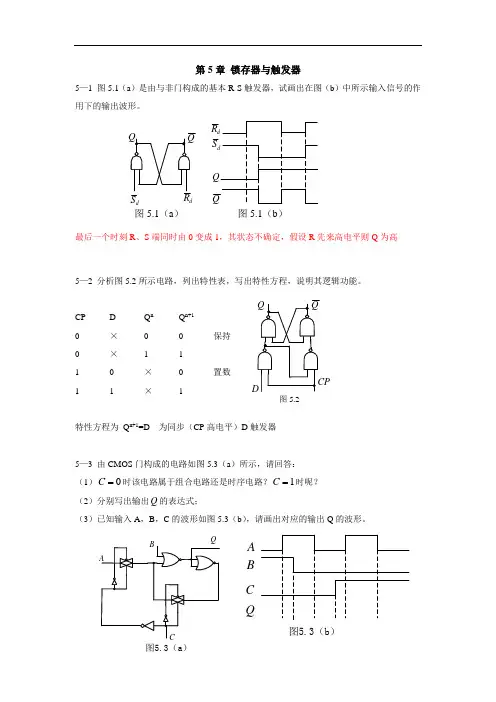
第5章锁存器与触发器5—1 图5.1(a)是由与非门构成的基本R-S触发器,试画出在图(b)中所示输入信号的作用下的输出波形。
dRdSQQ图 5.1(a)图 5.1(b)最后一个时刻R、S端同时由0变成1,其状态不确定,假设R先来高电平则Q为高5—2 分析图5.2所示电路,列出特性表,写出特性方程,说明其逻辑功能。
CP D Q n Q n+10 ×0 0 保持0 × 1 11 0 ×0 置数1 1 × 1特性方程为Q n+1=D 为同步(CP高电平)D触发器5—3 由CMOS门构成的电路如图5.3(a)所示,请回答:(1)0=C时该电路属于组合电路还是时序电路?1=C时呢?(2)分别写出输出Q的表达式;(3)已知输入A,B,C的波形如图5.3(b),请画出对应的输出Q的波形。
图5.2Q图5.3(a)ABCQ图5.3(b)答: 1) 0=C 时该电路属于组合电路(输出反馈截止)1时为时序电路。
2)C=0时 B A Q +=C=1时 n n n Q B Q B Q⋅=+=+15—4 已知CP 和D 的波形如图4.4所示,试对应画出习题5—2中电路的输出1Q 以及D 触发器(上升沿触发)的输出2Q 的波形。
(1Q 2Q 的初始状态为“0”5—5 今有两个TTL J-K 触发器,一个是主从触发方式,另一个是下降沿触发,已知两者的输入波形均如图5.5所示,试分别画出两个触发器的输出波形。
初始状态均为“0”。
对于主从JK 触发器,由于在CP 为1的全部时间内主触发器都可以接收输入信号,所以在CP 为1的期间输入信号发生变化后,CP 下降沿到达时从触发器的状态不一定按此刻输入信号的状态来确定,而必须考虑整个CP 为1期间内输入信号的变化过程才能确定触发器DQ QCPJQ Q 主从边沿A B C Q 图5.3(b)D Q Q的状态。
主从JK 触发器在Q 为0时主触发器只能接收置1输入信号,Q 为1时只能接收置0信号。

自我检查题5.1 时序电路和组合电路的根本区别是什么?同步时序电路与异步时序电路有何不同?解答:从功能上看,时序电路任何时刻的稳态输出不仅和该时刻的输入相关,而且还决定于该时刻电路的状态,从电路结构上讲,时序电路一定含有记忆和表示电路状态的存储器。
而组合电路任何时刻的稳态输出只决定于该时刻各个输入信号的取值,由常用门电路组成则是其电路结构的特点。
在同步时序电路中,各个触发器的时钟信号是相同的,都是输入CP 脉冲,异步时序电路则不同,其中有的触发器的时钟信号是输入cp 脉冲,有的则是其他触发器的输出,前者触发器的状态更新时同步的,后者触发器状态更新有先有后,是异步的。
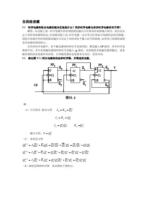
5.2 画出图T5.2所示电路的状态和时序图,并简述其功能。
图T5.2解:(1)写方程式 驱动方程 nQ K J 200==n Q K J 011==n n Q Q J 012=, n Q K 22=输出方程:nQ Y 2= (2) 求状态方程nn n n n n n n n n n Q Q Q Q Q Q Q Q Q K Q J Q 02020202000010+=+=+=+ n n n n n n n n n n n Q Q Q Q Q Q Q Q Q K Q J Q 01011010111111+=+=+=+ n n n n n n n n n n n Q Q Q Q Q Q Q Q Q K Q J Q 01222201222212=+=+=+(3)画状态图和时序图 状态图如下图所示:101时序图如下图所示:CP Q 0Q 1Q 25.3 试用边沿JK 触发器和门电路设计一个按自然态序进行计数的七进制同步加法计数器。
解:(1)状态图如下图:(2)求状态方程、输出方程CQ Q Q n n n /101112+++的卡诺图如下图所示:输出方程为nn Q Q C 12=状态方程:n n n n n Q Q Q Q Q 120112+=+ n n n n n n Q Q Q Q Q Q 0120111+=+ n n n n n Q Q Q Q Q 120110+=+驱动方程:n n n n n n n n n n n n n n n Q Q Q Q Q Q Q Q Q Q Q Q Q Q Q 0122120121220112)(++=++=+n n n n n n Q Q Q Q Q Q 1021011+=+n n n n n Q Q Q Q Q 0012101)(++=+与JK 触发器的特性方程 比较,可以得到驱动方程 n n Q Q J 012= 、 n Q K 12=n Q J 01= 、n n Q Q K 021=n n n n Q Q Q Q J 12120=+= 10=K(4) 无效状态转换情况 111/1000 能自启动(5) 逻辑图如下图所示:5.4 画出用时钟脉冲上升沿触发的边沿D 触发器组成的4位二进制异步加法计数器和减法计数器的逻辑电路图。
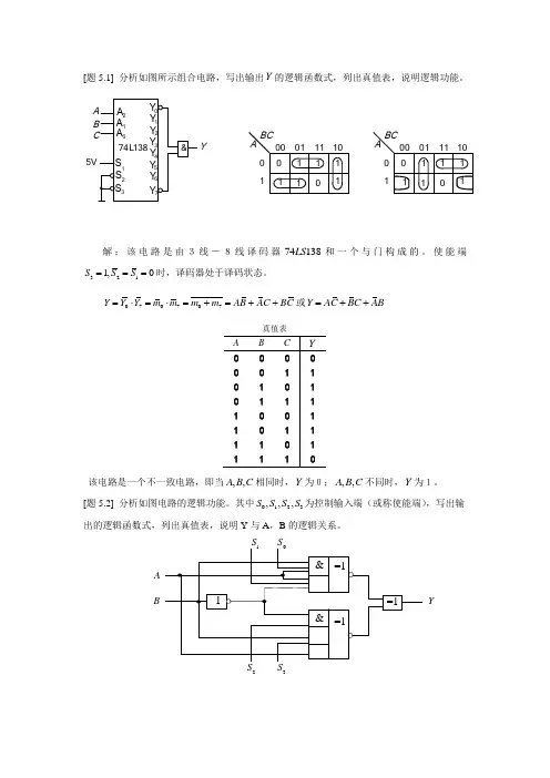
110001111001BC A111100110001111001BCA111100[题5.1] 分析如图所示组合电路,写出输出Y 的逻辑函数式,列出真值表,说明逻辑功能。
解:该电路是由3线-8线译码器74138LS 和一个与门构成的。
使能端3211,0S S S ===时,译码器处于译码状态。
070707Y Y Y m m m m AB AC BC =⋅=⋅=+=++或Y AC BC AB =++该电路是一个不一致电路,即当,,A B C 相同时,Y为0;,,A B C 不同时,Y 为1。
[题5.2] 分析如图电路的逻辑功能。
其中0123,,,S S S S 为控制输入端(或称使能端),写出输出的逻辑函数式,列出真值表,说明Y 与A ,B 的逻辑关系。
Y真值表23AB Y解:0123Y ABS ABS BS BS A =+⊕++[题5.5]试用与非门设计一个水坝水位控制器。
如图为水坝水位示意图。
A,B 为两个电极,当电极被水浸没时,会有输出信号。
如果水面在A 以下为正常状态,绿灯亮;水面在A 、B 间为异常状态,黄灯亮;水面在B 以上为危险状态,红灯亮。
解:(1)列真值表。
根据题意,该控制器有两个输入A,B ;三个输出,,G Y R ,G 代表绿灯,Y 代表黄灯,R代表红灯。
输入变量:水在电极之上,用1表示,水在电极之下,用0表示。
输出变量:1表示灯亮,0表示灯灭。
列出真制表。
(2)化简 G A = Y AB = R B =(3)逻辑图真值表B A B + 1 1 A BA BC00011110011010101A BC 00011110010111100[题5.8] 某学校有三个实验室,每个实验室各需2kW 电力。
这三个实验室由两台发电机组供电,一台是2kW ,另一台是4kW 。
三个实验室有时可能不同时工作,试设计一逻辑 电路,使资源合理分配。
解:(1)列真值表设输入变量为A 、B 、C 表示三个实验室,工作为1,不工作为0;设输出变量为1Y 、2Y ,分别表示2kW ,4kW 的发电机,启动为1,不启动为0。
C H A P T E R5T H E C M O S I N V E R T E R Quantification of integrity,performance,and energy metrics of an inverterOptimization of an inverter design5.1Exercises and Design Problems5.2The Static CMOS Inverter—An IntuitivePerspective5.3Evaluating the Robustness of the CMOSInverter:The Static Behavior5.3.1Switching Threshold5.3.2Noise Margins5.3.3Robustness Revisited5.4Performance of CMOS Inverter:The DynamicBehavior5.4.1Computing the Capacitances5.4.2Propagation Delay:First-OrderAnalysis5.4.3Propagation Delay from a DesignPerspective5.5Power,Energy,and Energy-Delay5.5.1Dynamic Power Consumption5.5.2Static Consumption5.5.3Putting It All Together5.5.4Analyzing Power Consumption UsingSPICE5.6Perspective:Technology Scaling and itsImpact on the Inverter Metrics180Section 5.1Exercises and Design Problems 1815.1Exercises and Design Problems1.[M,SPICE,3.3.2]The layout of a static CMOS inverter is given in Figure 5.1.(λ=0.125µm).a.Determine the sizes of the NMOS and PMOS transistors.b.Plot the VTC (using HSPICE)and derive its parameters (V OH ,V OL ,V M ,V IH ,and V IL ).c.Is the VTC affected when the output of the gates is connected to the inputs of 4similargates?.d.Resize the inverter to achieve a switching threshold of approximately 0.75V .Do not lay-out the new inverter,use HSPICE for your simulations.How are the noise margins affected by this modification?2.Figure 5.2shows a piecewise linear approximation for the VTC.The transition region isapproximated by a straight line with a slope equal to the inverter gain at V M .The intersectionof this line with the V OH and the V OL lines defines V IH and V IL .a.The noise margins of a CMOS inverter are highly dependent on the sizing ratio,r =k p /k n ,of the NMOS and PMOS e HSPICE with V Tn =|V Tp |to determine the valueof r that results in equal noise margins?Give a qualitative explanation.b.Section 5.3.2of the text uses this piecewise linear approximation to derive simplifiedexpressions for NM H and NM L in terms of the inverter gain.The derivation of the gain isbased on the assumption that both the NMOS and the PMOS devices are velocity saturatedat V M .For what range of r is this assumption valid?What is the resulting range of V M ?c.Derive expressions for the inverter gain at V M for the cases when the sizing ratio is justabove and just below the limits of the range where both devices are velocity saturated.What are the operating regions of the NMOS and the PMOS for each case?Consider theeffect of channel-length modulation by using the following expression for the small-signalresistance in the saturation region:r o,sat =1/(λI D ).Figure 5.1CMOS inverter layout.InOutGND V DD =2.5V.Poly Metal1NMOSPMOSPolyMetal12λ182THE CMOS INVERTER Chapter 53.[M,SPICE,3.3.2]Figure 5.3shows an NMOS inverter with resistive load.a.Qualitatively discuss why this circuit behaves as an inverter.b.Find V OH and V OL calculate V IH and V IL .c.Find NM L and NM H ,and plot the VTC using HSPICE.d.Compute the average power dissipation for:(i)V in =0V and (ii)V in =2.5Ve HSPICE to sketch the VTCs for R L =37k,75k,and 150k on a single graph.ment on the relationship between the critical VTC voltages (i.e.,V OL ,V OH ,V IL ,V IH )and the load resistance,R L .g.Do high or low impedance loads seem to produce more ideal inverter characteristics?4.[E,None,3.3.3]For the inverter of Figure 5.3and an output load of 3pF:a.Calculate t plh ,t phl ,and t p .b.Are the rising and falling delays equal?Why or why not?pute the static and dynamic power dissipation assuming the gate is clocked as fast as possible.5.The next figure shows two implementations of MOS inverters.The first inverter uses onlyNMOS transistors.V OH V OL inV outFigure 5.2A different approach to derive V IL and V IH .V outV in M 1W/L =1.5/0.5+2.5VFigure 5.3Resistive-load inverterR L =75k ΩSection 5.1Exercises and Design Problems183a.Calculate V OH ,V OL ,V M for each case.e HSPICE to obtain the two VTCs.You must assume certain values for the source/drain areas and perimeters since there is no layout.For our scalable CMOS process,λ =0.125μm,and the source/drain extensions are 5λfor the PMOS;for the NMOS the source/drain contact regions are 5λx5λ.c.Find V IH ,V IL ,NM L and NM H for each inverter and comment on the results.How can you increase the noise margins and reduce the undefined region?ment on the differences in the VTCs,robustness and regeneration of each inverter.6.Consider the following NMOS inverter.Assume that the bulk terminals of all NMOS deviceare connected to GND.Assume that the input IN has a 0V to 2.5V swing.a.Set up the equation(s)to compute the voltage on node x .Assume γ=0.5.b.What are the modes of operation of device M2?Assume γ=0.c.What is the value on the output node OUT for the case when IN =0V?Assume γ=0.d.Assuming γ=0,derive an expression for the switching threshold (V M )of the inverter.Recall that the switching threshold is the point where V IN =V OUT .Assume that the devicesizes for M1,M2and M3are (W/L)1,(W/L)2,and (W/L)3respectively.What are the limitson the switching threshold?For this,consider two cases:i)(W/L)1>>(W/L)2V DD =2.5V V IN V OUTV DD =2.5V V IN V OUT M 2M 1M 4M 3W/L=0.375/0.25W/L=0.75/0.25W/L=0.375/0.25W/L=0.75/0.25Figure 5.4Inverter ImplementationsV DD =2.5V OUTM1IN M2M3V DD =2.5Vx184THE CMOS INVERTER Chapter 5ii)(W/L)2>>(W/L)17.Consider the circuit in Figure 5.5.Device M1is a standard NMOS device.Device M2has allthe same properties as M1,except that its device threshold voltage is negative and has a valueof -0.4V.Assume that all the current equations and inequality equations (to determine themode of operation)for the depletion device M2are the same as a regular NMOS.Assume thatthe input IN has a 0V to 2.5V swing.a.Device M2has its gate terminal connected to its source terminal.If V IN =0V ,what is the output voltage?In steady state,what is the mode of operation of device M2for this input?pute the output voltage for V IN =2.5V .You may assume that V OUT is small to simplify your calculation.In steady state,what is the mode of operation of device M2for this input?c.Assuming Pr (IN =0)=0.3,what is the static power dissipation of this circuit?8.[M,None,3.3.3]An NMOS transistor is used to charge a large capacitor,as shown in Figure5.6.a.Determine the t pLH of this circuit,assuming an ideal step from 0to 2.5V at the input node.b.Assume that a resistor R S of 5k Ωis used to discharge the capacitance to ground.Deter-mine t pHL .c.Determine how much energy is taken from the supply during the charging of the capacitor.How much of this is dissipated in M1.How much is dissipated in the pull-down resistanceduring discharge?How does this change when R S is reduced to 1k Ω.d.The NMOS transistor is replaced by a PMOS device,sized so that k p is equal to the k n ofthe original NMOS.Will the resulting structure be faster?Explain why or why not.9.The circuit in Figure 5.7is known as the source follower configuration.It achieves a DC levelshift between the input and the output.The value of this shift is determined by the current I 0.Assume x d =0,γ=0.4,2|φf |=0.6V ,V T 0=0.43V ,k n ’=115μA/V 2and λ=0.V DD =2.5VOUTM1(4μm/1μm)IN M2(2μm/1μm),V Tn =-0.4VFigure 5.5A depletion load NMOSinverterV DD =2.5VOutFigure 5.6Circuit diagram with annotated W/L ratios=5pFSection 5.1Exercises and Design Problems 185a.Suppose we want the nominal level shift between V i and V o to be 0.6V in the circuit in Figure 5.7(a).Neglecting the backgate effect,calculate the width of M2to provide this level shift (Hint:first relate V i to V o in terms of I o ).b.Now assume that an ideal current source replaces M2(Figure 5.7(b)).The NMOS transis-tor M1experiences a shift in V T due to the backgate effect.Find V T as a function of V o for V o ranging from 0to 2.5V with 0.5V intervals.Plot V T vs.V oc.Plot V o vs.V i as V o varies from 0to 2.5V with 0.5V intervals.Plot two curves:one neglecting the body effect and one accounting for it.How does the body effect influence the operation of the level converter?d.At V o (with body effect)=2.5V,find V o (ideal)and thus determine the maximum error introduced by the body effect.10.For this problem assume:V DD =2.5V ,W P /L =1.25/0.25,W N /L =0.375/0.25,L =L eff =0.25μm (i.e.x d =0μm),C L =C inv-gate ,k n ’=115μA/V 2,k p ’=-30μA/V 2,V tn0=|V tp0|=0.4V,λ =0V -1, γ=0.4,2|φf |=0.6V ,and t ox =e the HSPICE model parameters for parasitic capacitance given below (i.e.C gd0,C j ,C jsw ),and assume that V SB =0V for all problems except part (e).Figure 5.7NMOS source follower configuration V DD =2.5V V iV oV DD =2.5VV i V oV bias =(a)(b)I o1um/0.25um M1186THE CMOS INVERTER Chapter 5##Parasitic Capacitance Parameters (F/m)##NMOS:CGDO=3.11x10-10,CGSO=3.11x10-10,CJ=2.02x10-3,CJSW=2.75x10-10PMOS:CGDO=2.68x10-10,CGSO=2.68x10-10,CJ=1.93x10-3,CJSW=2.23x10-10a.What is the V m for this inverter?b.What is the effective load capacitance C Leff of this inverter?(include parasitic capacitance,refer to the text for K eq and m .)Hint:You must assume certain values for the source/drain areas and perimeters since there is no layout.For our scalable CMOS process,λ =0.125μm,and the source/drain extensions are 5λfor the PMOS;for the NMOS the source/drain contact regions are 5λx5λ.c.Calculate t PHL ,t PLH assuming the result of (b)is ‘C Leff =6.5fF’.(Assume an ideal step input,i.e.t rise =t fall =0.Do this part by computing the average current used to charge/dis-charge C Leff .)d.Find (W p /W n )such that t PHL =t PLH .e.Suppose we increase the width of the transistors to reduce the t PHL ,t PLH .Do we get a pro-portional decrease in the delay times?Justify your answer.f.Suppose V SB =1V,what is the value of V tn ,V tp ,V m ?How does this qualitatively affect C Leff ?ing Hspice answer the following questions.a.Simulate the circuit in Problem 10and measure t P and the average power for input V in :pulse(0V DD 5n 0.1n 0.1n 9n 20n),as V DD varies from 1V -2.5V with a 0.25V interval.[t P =(t PHL +t PLH )/2].Using this data,plot ‘t P vs.V DD ’,and ‘Power vs.V DD ’.Specify AS,AD,PS,PD in your spice deck,and manually add C L =6.5fF.Set V SB =0Vfor this problem.b.For Vdd equal to 2.5V determine the maximum fan-out of identical inverters this gate candrive before its delay becomes larger than 2ns.c.Simulate the same circuit for a set of ‘pulse’inputs with rise and fall times of t in_rise,fall =1ns,2ns,5ns,10ns,20ns.For each input,measure (1)the rise and fall times t out_rise andV DD =2.5VV IN V OUTC L =C inv-gateL =L P =L N =0.25μmV SB-+(W p /W n =1.25/0.375)Figure 5.8CMOS inverter with capacitiveSection 5.1Exercises and Design Problems 187t out_fall of the inverter output,(2)the total energy lost E total ,and (3)the energy lost due to short circuit current E short .Using this data,prepare a plot of (1)(t out_rise +t out_fall )/2vs.t in_rise,fall ,(2)E total vs.t in_rise,fall ,(3)E short vs.t in_rise,fall and (4)E short /E total vs.t in_rise,fall.d.Provide simple explanations for:(i)Why the slope for (1)is less than 1?(ii)Why E short increases with t in_rise,fall ?(iii)Why E total increases with t in_rise,fall ?12.Consider the low swing driver of Figure 5.9:a.What is the voltage swing on the output node (V out )?Assume γ=0.b.Estimate (i)the energy drawn from the supply and (ii)energy dissipated for a 0V to 2.5V transition at the input.Assume that the rise and fall times at the input are 0.Repeat the analysis for a 2.5V to 0V transition at the input.pute t pLH (i.e.the time to transition from V OL to (V OH +V OL )/2).Assume the input rise time to be 0.V OL is the output voltage with the input at 0V and V OH is the output volt-age with the input at 2.5V .pute V OH taking into account body effect.Assume γ =0.5V 1/2for both NMOS and PMOS.13.Consider the following low swing driver consisting of NMOS devices M1and M2.Assumean NWELL implementation.Assume that the inputs IN and IN have a 0V to 2.5V swing andthat V IN =0V when V IN =2.5V and vice-versa.Also assume that there is no skew between INand IN (i.e.,the inverter delay to derive IN from IN is zero).a.What voltage is the bulk terminal of M2connected to?V in V out V DD =2.5V W L 3μm 0.25μm =p 2.5V0V C L =100fFW L 1.5μm 0.25μm=n Figure 5.9Low Swing DriverV LOW =0.5VOutM1ININ M225μm/0.25μm 25μm/0.25μmC L =1pFFigure 5.10Low Swing Driver188THE CMOS INVERTER Chapter 5b.What is the voltage swing on the output node as the inputs swing from 0V to 2.5V .Showthe low value and the high value.c.Assume that the inputs IN and IN have zero rise and fall times.Assume a zero skewbetween IN and IN.Determine the low to high propagation delay for charging the outputnode measured from the the 50%point of the input to the 50%point of the output.Assumethat the total load capacitance is 1pF,including the transistor parasitics.d.Assume that,instead of the 1pF load,the low swing driver drives a non-linear capacitor,whose capacitance vs.voltage is plotted pute the energy drawn from the lowsupply for charging up the load capacitor.Ignore the parasitic capacitance of the driver cir-cuit itself.14.The inverter below operates with V DD =0.4V and is composed of |V t |=0.5V devices.Thedevices have identical I 0and n.a.Calculate the switching threshold (V M )of this inverter.b.Calculate V IL and V IH of the inverter.15.Sizing a chain of inverters.a.In order to drive a large capacitance (C L =20pF)from a minimum size gate (with inputcapacitance C i =10fF),you decide to introduce a two-staged buffer as shown in Figure5.12.Assume that the propagation delay of a minimum size inverter is 70ps.Also assumeV DD =0.4VV IN V OUTFigure 5.11Inverter in Weak Inversion RegimeSection 5.1Exercises and Design Problems 189that the input capacitance of a gate is proportional to its size.Determine the sizing of thetwo additional buffer stages that will minimize the propagation delay.b.If you could add any number of stages to achieve the minimum delay,how many stages would you insert?What is the propagation delay in this case?c.Describe the advantages and disadvantages of the methods shown in (a)and (b).d.Determine a closed form expression for the power consumption in the circuit.Consider only gate capacitances in your analysis.What is the power consumption for a supply volt-age of 2.5V and an activity factor of 1?16.[M,None,3.3.5]Consider scaling a CMOS technology by S >1.In order to maintain compat-ibility with existing system components,you decide to use constant voltage scaling.a.In traditional constant voltage scaling,transistor widths scale inversely with S,W ∝1/S.To avoid the power increases associated with constant voltage scaling,however,youdecide to change the scaling factor for W .What should this new scaling factor be to main-tain approximately constant power.Assume long-channel devices (i.e.,neglect velocitysaturation).b.How does delay scale under this new methodology?c.Assuming short-channel devices (i.e.,velocity saturation),how would transistor widthshave to scale to maintain the constant power requirement?1InAdded Buffer StageOUTC L =20pF C i =10fF‘1’is the minimum size inverter.??Figure 5.12Buffer insertion for driving large loads.190THE CMOS INVERTER Chapter5DESIGN PROBLEMUsing the0.25μm CMOS introduced in Chapter2,design a static CMOSinverter that meets the following requirements:1.Matched pull-up and pull-down times(i.e.,t pHL=t pLH).2.t p=5nsec(±0.1nsec).The load capacitance connected to the output is equal to4pF.Notice that thiscapacitance is substantially larger than the internal capacitances of the gate.Determine the W and L of the transistors.To reduce the parasitics,useminimal lengths(L=0.25μm)for all transistors.Verify and optimize the designusing SPICE after proposing a first design using manual -pute also the energy consumed per transition.If you have a layout editor(suchas MAGIC)available,perform the physical design,extract the real circuitparameters,and compare the simulated results with the ones obtained earlier.。

第1章 数字电路基础知识1 电子电路主要分为两类:一类是电子电路主要分为两类:一类是 模拟电路 ,另一类是,另一类是 数字电路 。
2 模拟电路处理的是模拟电路处理的是 模拟信号 ,而数字电路处理的是,而数字电路处理的是 数字信号 。
3 晶体管(即半导体三极管)的工作状态有三种:晶体管(即半导体三极管)的工作状态有三种:截止截止、 放大和 饱和。
在模拟电路中,晶体管主要工作在体管主要工作在 放大状态 。
4 在数字电路中,晶体管工作在在数字电路中,晶体管工作在 截止与 饱和状态,也称为状态,也称为 “开关”状态。
状态。
5 模拟信号是一种模拟信号是一种大小随时间连续变化大小随时间连续变化的电压或电流,数字信号是一种的电压或电流,数字信号是一种突变突变的电压和电流。
6 模拟信号的电压或电流的大小是模拟信号的电压或电流的大小是随时间连续缓慢变化的随时间连续缓慢变化的,而数字信号的特点是“保持”(一段时间内维持低电压或高电压)和“段时间内维持低电压或高电压)和“突变突变”(低电压与高电压的转换瞬间完成)。
7 在数字电路中常将0~1v 范围的电压称为范围的电压称为低电平低电平,用,用““0”来表示;将3~5v 范围的电压称为高电平,用,用““1”来表示。
来表示。
介绍了数字电路的发展状况和数字电路的一些应用领域,并将数字电路和模拟电路进行了比较,让读者了解两者的区别,以利于后面数字电路的学习。
以利于后面数字电路的学习。
第2章 门电路1 基本门电路有基本门电路有与门与门、或门、非门三种。
三种。
2 与门电路的特点是:只有输入端都为只有输入端都为 高电平 时,输出端才会输出高电平;只要有一个输入端为“0”,输出端就会输出输出端就会输出 低电平 。
与门的逻辑表达式是与门的逻辑表达式是 Y A B =· 。
3 或门电路的特点是:只要有一个输入端为只要有一个输入端为 高电平 ,输出端就会输出高电平。
只有输入端都为 低电平 时,输出端才会输出低电平。
第1章习题1.1 名词解释PROM CPLD FPGA ASICJTAG边界扫描FPGA/CPLD编程与配置逻辑综合PAL EDA GAL IP-CORE ISP ASIC RTL FPGA SOPC CPLDIP-CORE SOC和SOPC EDA/CAD1.2 现代EDA技术的特点有哪些?采用HDL描述、自顶向下、开放标准、具有完备设计库1.3 什么是Top-down设计方式?(P4)1.4 数字系统的实现方式有哪些?各有什么优缺点?74LS系列/4000系列常规逻辑门设计:设计难度大、调试复杂采用CPLD/FPGA等可编程器件来设计:用HDL描述、设计难度小、调试仿真方便,开发费用低,但单位成本较高,适合小批量应用专用集成电路设计:设计掩模成本高,适合大批量应用1.5什么是IP复用技术?IP核对EDA技术的应用和发展有什么意义?(P5)IP可重复使用的一种功能设计,可节省设计时间、缩短开发周期,避免重复劳动为大规模SOC设计提供开发基础、和开发平台。
1.6 用硬件描述语言设计数字电路有什么优势?优势:可进行行为级、RTL级、门级多层面对电路进行描述、可功能仿真时序分析,与工艺无关。
1.8 基于FPGA/CPLD的数字系统设计流程包括哪些步骤?(P8 图1.7)1.9 什么是综合?常用的综合工具有哪些?HDL→RTL→门级→网表的描述转换过程ALTERA:MAX-PLUSII,Quartus, Xilinx:ISE , Lattice: ispLERVER1.10 功能仿真与时序仿真有什么区别?功能仿真不考虑器件延时,而时序分析必须考虑在不同器件中的物理信号的延时1.11 数字逻辑设计描述分哪几个层级,各有什么特点。
1.12、为何任意组合逻辑电路可用通用的与阵列、或阵列组合来实现。
可表示为布尔代数方程,由乘积项的和表示1.13 FPGA与CPLD在实现方式或内部结构上的主要区别查表、与或阵列1.14 VerilogHDL与计算机程序设计语言主要区别(描述并行电路行为或结构、描述的串行指令流)1.15 简述“逻辑综合”功能作用。
CHAPTER 5P5.1. For each problem, restate each Boolean equation into a form such that it can be translatedinto the p and n-complex of a CMOS gate.a. ()()Out ABC BD ABC BD A B C B D =+=+=+++b. ()()()Out AB AC BC AB AC BC A B A C B C =++=++=+++c. ()()Out A B CD A AB C D A A B CD A A B CD A =+++=++=+++=++AbVddVddAb BbAAbVddP5.2.AP5.3. First, convert the equation into its p and n-complex.()()()()()()()()()()()Out A B C BC AB AB C BC AB AB C BC AB AB C BC AB AB C BC AB AB C B C =⊕+=++=++=+=++=+++VddP5.4. The truth table is given below in terms of voltages. The function is F A B =The worse case V OH is V DD and the worse case V OL is 0V.P5.5. The first circuit is a NOR gate while the second is a NAND gate. The V OL and V OHcalculated are for the worst-case scenario. To find this, assume only one transistor turns on, this just reduces to a pseudo-NMOS/PMOS inverter, so the other transistors are not important.a. The V OL for the pseudo-NMOS (in 0.18μm) is:()()()2,1N N OXNSAT OX P GSP TPP SATOL W C L N DD TN GSP TP CP PDD TN SAT P N OX v C W V V I V k V V V V E L V V v W L C μ-==--+-=()2DD TP N N OX V V W C μ-()()()()()20.1DD TP CP P DD TN SAT P N DD TPDDN N DD TP CP P DD TN V V E L V V v W L V V V W V V E L V V μ-+--==-+-()()()()()()()()()()()()226440.18100.2100.210 1.80.50.14μm=1.40.11.8270 1.80.5240.2 1.80.5SAT P N DD TPN DD N DD TP CP P DD TN v W L V V W V V V E L V V μλ---=-+-⨯⨯⨯-==-+-Since the minimum width is 2λ, we make that the width. The V OH for the pseudo-PMOS (in 0.18μm) is:()()()()()()2221SDPSDP CP PN P V P OX P SGP TP SDP SAT OX N GSN TN V GSN TN CN N N E L SAT OX I sat I lin C W V V V v C W V V V V E L L v C μ=---=-++()2P OX N DD TN DD TN CN NC W V V V V E L μ-=-+()()()()()()2201DD OH DD OH CP PV V P DD TPDDOH V V P E L W V V VV L ------+()()()()()()20.1824620.184.8(70) 1.80.50.180.2(10)(810)1.80.51.80.5 1.21P P W L ---⨯-=-++4.2P W λ≈The pseudo-PMOS circuit will have bigger devices than the pseudo-NMOS.P5.6. The steps to solving this question are the same as the pseudo-NMOS question in Chapter4.a. For V OH , recognize that GS T V V >= for operation so the output can only be as high asDD T V V -. Since 0SB V ≠, body effect must be taken into account and the full equationis:()()()001.20.40.2OH DD T DDT V V V V Vγγ=-+=-+=-+ Iteration produces V OH =0.73V.b. For V OL , we must first recognize that the worst-case V OL occurs when only one of the pull-down transistors is on. Next we identify the regions of operation of the transistors. In this case, the pull-up transistor is always in saturation and the pull-down is most likely in the linear region since it will have a high input (high V GS ) and a low output (low V DS ). Then, we equate the two currents together and solve for V OL :()()()()()()()()221222222211111224620.61(1)(270)1.20.4(0.13)(10)(810)1.20.42(1.20.42)0.61DS DS CN OL OLV N OX GS T DS sat OX GS T V GS T CN E LV OL OL V OL I sat I lin W C V V V W v C V V V V E LL V V V μ-=---=-++--⨯--=--++Using a programmable calculator or a spreadsheet program, V OL = 0.205V. The dc current with the output low is:()()()()2222222260.20520.2050.61(1)(270)(1.610)1.20.4(0.205)146.5DS DS CN V N OX GS T DS DS V ELW C V V V I L Aμμ---=+⨯--=+=The power with the output low is:(46.5)(1.2)55.8DS DD P I V A V W μμ===P5.7. See Example 5.2 which is based on the NAND gate. This question is the same except thatit addresses the NOR gate.With both inputs tied together, 88N P W W λλ==2χ=== ()()1.80.520.50.77V 112DD TP TNS V V V V χχ-+-+===++In the SPICE solution, the reason why the results vary for input A and B is due to body-effect.P5.8. The solution is shown below. Notice that there is no relevance with the lengths andwidths of the transistors when it comes to V OH , although they the do matter when calculating V OL.01.80.50.3 2.51Vout GG T GG out T V V V V V V γ=-=++=++=P5.9. For t PLH , we need to size the pull-up PMOS appropriately.()()()()15120.70.720.70.73010010845010PLH eqp LOAD p SQLOAD PLHLt RC R C WL W R C k t λλ--====Ω⨯=⨯For V OL :()()()()()()()()()()()()()2246660.1220.10.63 4.210810 1.610 1.20.4 1.08mA1.20.4240.1(270)(1.610)1.20.40.11138.577377232(3OLOL CN P sat OX GS T P GS T CP V N N OX OL TN OLN P V N N E LNN NW v C V V I sat V V E LW C V V V W I sat L L W W W stack L μλλλ---⨯⨯⨯--===-+-+--⨯--==++===⨯=2)155(2)W stack λ=P5.10. The circuit is shown below:()()()()()()()()31512315120.720.70.7301075106350100.720.70.712.510751026.6275010PLH EQP LOAD PP EQPLOAD PLHPHL EQN LOAD NN EQNLOAD PHLLt RC R C W L W R C t Lt RC R C W L W R C t λλλλλ----====⨯⨯=⨯====⨯⨯=≈⨯Because the number of transistors in series is more than one, we must multiply the widths by the appropriate number. Here, all the NMOS transistors will have a width of 54λ. The PMOS transistors will have widths of 126λ and 190λ, respectively.P5.11. We estimate the dc power and dynamic switching power for this problem.a. The circuit’s dc power can be computed by computing the dc current when the output is low. This is given by I DS =550uA/um x 0.1um=55uA. Then P DC =66uW when the output is low.b. Its dynamic power can be calculated by simply using the equation 2dyn DD P CV f α=. Therefore, P dyn =(50fF)(V DD -V TN )(V DD )(100MHz)=4.4uW.P5.12. The pseudo-NMOS inverter has static current when the output is low. We can estimate itas:()()()()()()()()224660.110810 1.610 1.20.425.6A 1.20.4240.1P sat OX GS T P GS T CP W v C V V I sat V V E Lμ--⨯⨯⨯--===-+-+Then the average static power is P stat =(25.6uA)(1.2)/2 =15.4uW.The dynamic power is dyn DD swing avg P CV V f ==(50fF)(1.2)(1.1)f avg assuming that V OL is 0.1V.For the CMOS inverter, the static power is almost zero: P stat =I sub V DD . It is far less than the pseudo-NMOS case. The dynamic power dyn DD swing avg P CV V f ==(50fF)(1.2)2f avg is slightly larger than the pseudo-NMOS case.VVINCMOS InverterV V INPseudo-NMOSP5.13. Model development to compute αsc .P5.14. The energy delivered by the voltage source is:()()200202DDDDV C sourceDD DD L L DDCL DDV CDDcap C LC L C C LdvE i t V dt V C dt C V dvC V dt dv V E i t v dt C v dt C v dv C dt∞∞∞∞========⎰⎰⎰⎰⎰⎰As can be seen, only half the energy is stored in the capacitor. The other half was dissipated as heat through the resistor.P5.15. The average dynamic power does not depend on temperature if the frequency stays thesame. However, the short-circuit current will increase as temperature increases. In addition, the subthreshold current increases as temperature increases. So the overall power dissipation will be higher. P5.16. The circuit is shown below. The delay should incorporate both Q and Qb settling in400ps. All NMOS and PMOS devices are the same size in both NAND gates.QQW()()()()()()()()15331220.70.70.70.720.71001030100.1212.5100.10.72400101μm N P P PHL PLH UP LOAD DOWN LOAD LOAD eqp eqn P N LOAD eqp eqn LOAD eqp eqn PL Lt t t R C R C C R R W W C R L R L WC R L R L W t --⎛⎫=+=+=+ ⎪⎝⎭+=++==≈P5.17. The small glitch in J propagates through the flop even though it is small. This is due tothe fact that the JK-flop of Figure 5.20 has the 1’s catching problem. P5.18. The small glitch in J does not propagate through the flop since the edge-triggeredconfiguration does not have a 1’s catching problem.P5.19. The positive-edge triggered FF is as follows:QQDS(a) With CK=D=0 and S=R=1, the outputs are(b) Now CK=0。
5.11画出图P5.11电路Q端的波形。
设初态为“0”。
图P5.14 图P5.15 5.15 画出图P5.15电路中Q端的波形。
解:Q 端波形如图P5.15所示。
5.16 试作出图P5.16电路中Q A 、Q B 的波形。
解:Q 端波形如图P5.16所示。
R D CP CP ⊕Q 2
Q 1Q 2
A R D
B Q A
Q B
图P5.16 图P5.17
5.17 试作出图P5.17电路中Q 1、Q 2 的波形。
解:Q 端波形如图P5.17所示。
5.18 试作出图P5.18电路中Q 1和Q 2的波形(设Q 1和Q 2的初态均为“0”),并说明Q 1和
Q 2对于CP 2各为多少分频。
解:Q 端波形如图P5.18所示。
Q 1和Q 2对于CP 2都是4分频,即
图P5.18 图P5.19
5.19 已知电路如图P5.19,试作出Q 端的波形。
设Q 的初态为“0”。
解:Q 端波形如图P5.19所示。
5.20 已知输入u I 、输出u O 波形分别如图P5.20所示,试用两个D 触发器将该输入波形u I
转换成输出波形u O 。
解:实现电路如图P5.20所示。
图P5.20
?)
?,(2
22
1==CP Q CP Q f f f f CP 2CP 1Q 1Q 2
CP A Q
u I
u O。
第1章习题及解答1.1 将下列二进制数转换为等值的十进制数。
(1)(11011)2 (2)(10010111)2(3)(1101101)2 (4)(11111111)2(5)(0.1001)2(6)(0.0111)2(7)(11.001)2(8)(101011.11001)2题1.1 解:(1)(11011)2 =(27)10 (2)(10010111)2 =(151)10(3)(1101101)2 =(109)10 (4)(11111111)2 =(255)10(5)(0.1001)2 =(0.5625)10(6)(0.0111)2 =(0.4375)10(7)(11.001)2=(3.125)10(8)(101011.11001)2 =(43.78125)10 1.3 将下列二进制数转换为等值的十六进制数和八进制数。
(1)(1010111)2 (2)(110111011)2(3)(10110.011010)2 (4)(101100.110011)2题1.3 解:(1)(1010111)2 =(57)16 =(127)8(2)(110011010)2 =(19A)16 =(632)8(3)(10110.111010)2 =(16.E8)16 =(26.72)8(4)(101100.01100001)2 =(2C.61)16 =(54.302)81.5 将下列十进制数表示为8421BCD码。
(1)(43)10 (2)(95.12)10(3)(67.58)10 (4)(932.1)10题1.5 解:(1)(43)10 =(01000011)8421BCD(2)(95.12)10 =(10010101.00010010)8421BCD(3)(67.58)10 =(01100111.01011000)8421BCD(4)(932.1)10 =(100100110010.0001)8421BCD1.7 将下列有符号的十进制数表示成补码形式的有符号二进制数。
第5章 习题解答5-1 由与非门组成的大体RS 触发器的d d S ,R 之间什么缘故要有约束?当违背约束条件时,输出端Q 、Q 会显现什么情形?试举例说明。
解:由与非门组成的大体RS 触发器的d R 和d S 之间的约束条件是:不许诺d R 和d S 同时为0。
当违背约束条件即当d R =d S =0时,Q 、Q 端将同时为1,作为大体存储单元来讲,这既不是0状态,又不是1状态,没成心义。
5-2 试列出或非门组成的大体RS 触发器的真值表,它的输入端R d 和S d 之间是不是也要有约束?什么缘故?解:真值表如右表所示、Rd 、Sd 之同也要有约束条件,即不许诺Rd=Sd=1, 不然Q 、Q 端会同时显现低电平。
5-3 画出图5-33由与非门组成的大体RS 触发器输出端Q 、Q 的电压波形,输入端D D S R 、的电压波形如图中所示。
图5-33解:见以下图:5-4 画出图5-34由或非门组成的大体RS触发器输出端Q、Q的电压波形,输入端S D、R D的电压波形如图中所示。
图5-34解:见以下图:5-5 图5-35所示为一个防抖动输出的开关电路。
当拨动开关S时,由于开关触点接通R S、的电压波形如图中所示。
试画出Q、Q端对应的电压波形。
刹时发生振颤,D D图5-35解:见以下图:5-6 在图5-36电路中、假设CP、S、R的电压波形如图中所示,试画出Q、Q端与之对应的电压波形。
假定触发器的初始状态为Q=0。
图5-36解:见以下图:5-7 在图5-37(a)所示的主从RS触发器中,CP、R、S的波形如图5-37(b)所示,试画Q、Q和Q的波形图。
出相应的Q m、m图5-37解:主从RS触发器的工作进程是:在CP=l期间主触发器接收输入信号,但输出端并非改变状态,只有当CP下降沿到来时从触发器甚才翻转,称为下降沿触发。
依照主从RS 触发器状态转换图可画出波形图如下图所示。
5-8 在图5-38(a)所示的主从JK触发器中,CP、J、K的波形如图5-38(b)所示,试画Q、Q和Q的波形图。
画出图电路Q端的波形。
设初态为“0”。
图图画出图电路中Q端的波形。
解:Q端波形如图所示。
试作出图电路中Q A、Q B的波形。
解:Q端波形如图所示。
R D
CP CP⊕Q2
Q1
Q2
A
D
B
Q
A
Q
B
图图
试作出图电路中Q1、Q2的波形。
解:Q端波形如图所示。
试作出图电路中Q1和Q2的波形(设Q1和Q2的初态均为“0”),并说明Q1和Q2对于CP2各为多少分频。
解:Q端波形如图所示。
Q1和Q2对于CP2都是4分频,即
图图
已知电路如图,试作出Q端的波形。
设Q的初态为“0”。
解:Q端波形如图所示。
已知输入u
I 、输出u
O
波形分别如图所示,试用两个D触发器将该输入波形u
I
转换成输出波
形u
O。
解:实现电路如图所示。
?)
?,
(
2
2
2
1=
=
CP
Q
CP
Q
f
f
f
f
CP2 CP1 Q1
Q2CP A Q
u I
u
O
图。