芯嵌stm32开发板原理图V3.0版本
- 格式:pdf
- 大小:66.30 KB
- 文档页数:1

UM0723User manual1 kW three-phase motor control demonstration boardfeaturing L6390 drivers and STGP10NC60KD IGBT 1 IntroductionThis document describes the 1 kW three-phase motor control demonstration board featuringthe L6390 high and low-side drivers and the STGP10NC60KD IGBT. The demonstrationboard is an AC/DC inverter that generates a three-phase waveform for driving three or two-phase motors such as induction motors or PMSM motors up to 1000 W with or withoutsensors.The main device presented in this user manual is a universal, fully evaluated, and populateddesign consisting of a three-phase inverter bridge based on the 600 V STMicroelectronics™IGBT STGP10NC60KD in a TO-220 package mounted on a heatsink, and the L6390 high-voltage high-side and low-side driver featuring an integrated comparator for hardwareprotection features such as overcurrent and overtemperature. The driver also integrates anoperational amplifier suitable for advanced current sensing. Thanks to this advancedcharacteristic, the system has been specifically designed to achieve an accurate and fastconditioning of the current feedback, therefore matching the typical requirements in fieldoriented control (FOC).The board has been designed to be compatible with single-phase mains, supplying from90 VAC to 285 VAC or from 125 VDC to 400 VDC for DC voltage. With reconfiguration of theinput sourcing, the board is suitable also for low-voltage DC applications up to 35 VDC. Thisdocument is associated with the release of the STEVAL-IHM023V2 demonstration board(see Figure1 below).Figure 1.STEVAL-IHM023V2June 2011Doc ID 15870 Rev 41/48Contents UM0723Contents1Introduction . . . . . . . . . . . . . . . . . . . . . . . . . . . . . . . . . . . . . . . . . . . . . . . . 12System introduction . . . . . . . . . . . . . . . . . . . . . . . . . . . . . . . . . . . . . . . . . 62.1Main characteristics . . . . . . . . . . . . . . . . . . . . . . . . . . . . . . . . . . . . . . . . . . 62.2Target applications . . . . . . . . . . . . . . . . . . . . . . . . . . . . . . . . . . . . . . . . . . . 62.3Safety and operating instructions . . . . . . . . . . . . . . . . . . . . . . . . . . . . . . . . 72.3.1General terms . . . . . . . . . . . . . . . . . . . . . . . . . . . . . . . . . . . . . . . . . . . . . 72.3.2Demonstration board intended use . . . . . . . . . . . . . . . . . . . . . . . . . . . . . 72.3.3Demonstration board installation . . . . . . . . . . . . . . . . . . . . . . . . . . . . . . . 72.3.4Electrical connections . . . . . . . . . . . . . . . . . . . . . . . . . . . . . . . . . . . . . . . 82.3.5Demonstration board operation . . . . . . . . . . . . . . . . . . . . . . . . . . . . . . . . 83Board description . . . . . . . . . . . . . . . . . . . . . . . . . . . . . . . . . . . . . . . . . . . 93.1System architecture . . . . . . . . . . . . . . . . . . . . . . . . . . . . . . . . . . . . . . . . . . 93.2The board schematic . . . . . . . . . . . . . . . . . . . . . . . . . . . . . . . . . . . . . . . . 103.3Circuit description . . . . . . . . . . . . . . . . . . . . . . . . . . . . . . . . . . . . . . . . . . . 163.3.1Power supply . . . . . . . . . . . . . . . . . . . . . . . . . . . . . . . . . . . . . . . . . . . . . 163.3.2Inrush limitation . . . . . . . . . . . . . . . . . . . . . . . . . . . . . . . . . . . . . . . . . . . 173.3.3Brake function . . . . . . . . . . . . . . . . . . . . . . . . . . . . . . . . . . . . . . . . . . . . 173.3.4Gate driving circuit . . . . . . . . . . . . . . . . . . . . . . . . . . . . . . . . . . . . . . . . . 183.3.5Overcurrent protection . . . . . . . . . . . . . . . . . . . . . . . . . . . . . . . . . . . . . . 183.3.6Current sensing amplifying network . . . . . . . . . . . . . . . . . . . . . . . . . . . . 193.3.7The tachometer and Hall/encoder inputs . . . . . . . . . . . . . . . . . . . . . . . . 233.3.8Temperature feedback and overtemperature protection . . . . . . . . . . . . 234Hardware setting of the STEVAL-IHM023V2 . . . . . . . . . . . . . . . . . . . . . 244.1Hardware settings for six-step (block commutation) control of BLDCmotors . . . . . . . . . . . . . . . . . . . . . . . . . . . . . . . . . . . . . . . . . . . . . . . . . . . 244.2Hardware settings for “Field Oriented Control” (FOC) in single-shunttopology current reading configuration . . . . . . . . . . . . . . . . . . . . . . . . . . . 264.3Hardware settings for FOC in three-shunt configuration . . . . . . . . . . . . . 27 5Description of jumpers, test pins, and connectors . . . . . . . . . . . . . . . 302/48Doc ID 15870 Rev 4UM0723Contents 6Connector placement . . . . . . . . . . . . . . . . . . . . . . . . . . . . . . . . . . . . . . . 33 7Bill of material . . . . . . . . . . . . . . . . . . . . . . . . . . . . . . . . . . . . . . . . . . . . . 34 8PCB layout . . . . . . . . . . . . . . . . . . . . . . . . . . . . . . . . . . . . . . . . . . . . . . . . 40 9Ordering information . . . . . . . . . . . . . . . . . . . . . . . . . . . . . . . . . . . . . . . 44 10Using STEVAL-IHM023V2 with STM32 PMSM FOC firmwarelibrary v3.0 . . . . . . . . . . . . . . . . . . . . . . . . . . . . . . . . . . . . . . . . . . . . . . . . 4410.1Environmental considerations . . . . . . . . . . . . . . . . . . . . . . . . . . . . . . . . . 4410.2Hardware requirements . . . . . . . . . . . . . . . . . . . . . . . . . . . . . . . . . . . . . . 4510.3Software requirements . . . . . . . . . . . . . . . . . . . . . . . . . . . . . . . . . . . . . . . 4510.4STM32 FOC firmware library v3.0 customization . . . . . . . . . . . . . . . . . . . 45 11Conclusion . . . . . . . . . . . . . . . . . . . . . . . . . . . . . . . . . . . . . . . . . . . . . . . . 47 12References . . . . . . . . . . . . . . . . . . . . . . . . . . . . . . . . . . . . . . . . . . . . . . . . 47 13Revision history . . . . . . . . . . . . . . . . . . . . . . . . . . . . . . . . . . . . . . . . . . . 47Doc ID 15870 Rev 43/48List of tables UM0723 List of tablesTable 1.Current reading configuration. . . . . . . . . . . . . . . . . . . . . . . . . . . . . . . . . . . . . . . . . . . . . . . 23 Table 2.Jumper settings for high-voltage BLDC motor in six-step control. . . . . . . . . . . . . . . . . . . . 24 Table 3.Jumper settings for low-voltage BLDC motor in six-step control . . . . . . . . . . . . . . . . . . . . 25 Table 4.Jumper settings for high-voltage PMAC or generic AC motor in single-shuntFOC control . . . . . . . . . . . . . . . . . . . . . . . . . . . . . . . . . . . . . . . . . . . . . . . . . . . . . . . . . . . . 26 Table 5.Jumper settings for low-voltage BLDC motor in single-shunt FOC control. . . . . . . . . . . . . 27 Table 6.Jumper settings for FOC of HV PMSM, BLDC, or AC IM in three-shunt configuration for current reading . . . . . . . . . . . . . . . . . . . . . . . . . . . . . . . . . . . . . . . . . . . . . . . . . . . . . . . 28 Table 7.Jumper settings for FOC of LV PMSM or BLDC in three-shunt configuration for current reading . . . . . . . . . . . . . . . . . . . . . . . . . . . . . . . . . . . . . . . . . . . . . . . . . . . . . . . . . . 29 Table 8.Jumpers description . . . . . . . . . . . . . . . . . . . . . . . . . . . . . . . . . . . . . . . . . . . . . . . . . . . . . . 30 Table 9.Connector pinout description . . . . . . . . . . . . . . . . . . . . . . . . . . . . . . . . . . . . . . . . . . . . . . . 31 Table 10.Testing pins description . . . . . . . . . . . . . . . . . . . . . . . . . . . . . . . . . . . . . . . . . . . . . . . . . . . 32 Table 11.Bill of material. . . . . . . . . . . . . . . . . . . . . . . . . . . . . . . . . . . . . . . . . . . . . . . . . . . . . . . . . . . 34 Table 12.STEVAL-IHM023V2 motor control workbench parameters . . . . . . . . . . . . . . . . . . . . . . . . 45 Table 13.Document revision history . . . . . . . . . . . . . . . . . . . . . . . . . . . . . . . . . . . . . . . . . . . . . . . . . 47 4/48Doc ID 15870 Rev 4UM0723List of figures List of figuresFigure 1.STEVAL-IHM023V2 . . . . . . . . . . . . . . . . . . . . . . . . . . . . . . . . . . . . . . . . . . . . . . . . . . . . . . . 1 Figure 2.Motor control system architecture. . . . . . . . . . . . . . . . . . . . . . . . . . . . . . . . . . . . . . . . . . . . . 9 Figure 3.STEVAL- IHM023V2 schematic - part 1. . . . . . . . . . . . . . . . . . . . . . . . . . . . . . . . . . . . . . . 10 Figure 4.STEVAL- IHM023V2 schematic - part 2. . . . . . . . . . . . . . . . . . . . . . . . . . . . . . . . . . . . . . . 11 Figure 5.STEVAL- IHM023V2 schematic - part 3. . . . . . . . . . . . . . . . . . . . . . . . . . . . . . . . . . . . . . . 12 Figure 6.STEVAL- IHM023V2 schematic - part 4. . . . . . . . . . . . . . . . . . . . . . . . . . . . . . . . . . . . . . . 13 Figure 7.STEVAL- IHM023V2 schematic - part 5. . . . . . . . . . . . . . . . . . . . . . . . . . . . . . . . . . . . . . . 14 Figure 8.STEVAL- IHM023V2 schematic - part 6. . . . . . . . . . . . . . . . . . . . . . . . . . . . . . . . . . . . . . . 15 Figure 9.Power supply block diagram. . . . . . . . . . . . . . . . . . . . . . . . . . . . . . . . . . . . . . . . . . . . . . . . 17 Figure 10.Gate driving network. . . . . . . . . . . . . . . . . . . . . . . . . . . . . . . . . . . . . . . . . . . . . . . . . . . . . . 18 Figure 11.Overcurrent protection . . . . . . . . . . . . . . . . . . . . . . . . . . . . . . . . . . . . . . . . . . . . . . . . . . . . 19 Figure 12.Three-shunt configuration. . . . . . . . . . . . . . . . . . . . . . . . . . . . . . . . . . . . . . . . . . . . . . . . . . 21 Figure 13.Six-step current sensing configuration . . . . . . . . . . . . . . . . . . . . . . . . . . . . . . . . . . . . . . . . 22 Figure 14.NTC placement on the heatsink. . . . . . . . . . . . . . . . . . . . . . . . . . . . . . . . . . . . . . . . . . . . . 23 Figure 15.STEVAL-IHM023V2 connectors placement . . . . . . . . . . . . . . . . . . . . . . . . . . . . . . . . . . . . 33 Figure 16.Silk screen - top side . . . . . . . . . . . . . . . . . . . . . . . . . . . . . . . . . . . . . . . . . . . . . . . . . . . . . 41 Figure 17.Silk screen - bottom side . . . . . . . . . . . . . . . . . . . . . . . . . . . . . . . . . . . . . . . . . . . . . . . . . . 42 Figure 18.Copper tracks - top side . . . . . . . . . . . . . . . . . . . . . . . . . . . . . . . . . . . . . . . . . . . . . . . . . . . 43 Figure 19.Copper tracks - bottom side . . . . . . . . . . . . . . . . . . . . . . . . . . . . . . . . . . . . . . . . . . . . . . . . 43Doc ID 15870 Rev 45/48System introduction UM07236/48Doc ID 15870 Rev 42 System introduction2.1 Main characteristicsThe information below lists the converter specification data and the main parameters set forthe STEVAL-IHM023V2 demonstration board.●Minimum input voltage 125 VDC or 90 VAC ●Maximum input voltage 400 VDC or 285 VAC●With applied input voltage doubler - the range is from 65 VAC to 145 VAC ●Voltage range for low-voltage motor control applications from 18 VDC to 35 VDC ●Possibility to use auxiliary +15 V supply voltage ●Maximum output power for motors up to 1000 W ●Regenerative brake control feature ●Input inrush limitation with bypassing relay●+ 15 V auxiliary power supply based on buck converter with VIPer™16●IGBT power switch STGP10NC60KD in TO-220 package - compatible with other ST IGBTs or power MOSFETs in TO-220 package●Fully populated board conception with testing points and isolated plastic safety cover ●Motor control connector for interface with STM3210B-EVAL board and other ST motor control dedicated kits ●Tachometer input ●Hall/encoder inputs●Possibility to connect BEMF daughterboard for sensorless six-step control of BLDC motors●PCB type and size:–Material of PCB - FR-4–Double-sided layout –Copper thickness: 60 µm–T otal dimensions of demonstration board: 127 mm x 180 mm.2.2 Target applications●Washing machines ●Home appliances●Medical applications - rehabilitative beds●High-power, high-efficiency water pumps for heating applications.UM0723System introductionDoc ID 15870 Rev 47/482.3 Safety and operating instructions2.3.1 General termsWarning:During assembly, testing, and operation, the demonstrationboard poses several inherent hazards, including bare wires, moving or rotating parts, and hot surfaces. There is a danger of serious personal injury and damage to property, if the kit or components are improperly used or installed incorrectly. The kit is not electrically isolated from the AC/DC input. The demonstration board is directly linked to the mains voltage. No insulation has been placed between the accessible parts and the high-voltage. All measurement equipment must be isolated from the mains before powering the board. When using an oscilloscope with the demonstration board, it must be isolated from the AC line. This prevents a shock from occurring as a result of touching any single point in the circuit, but does NOT prevent shocks when touching two or more points in the circuit. Do not touch the demonstration board after disconnection from the voltage supply, as several parts and power terminals, which contain energized capacitors, need to be allowed to discharge.All operations involving transportation, installation and use, as well as maintenance, are to be carried out by skilled technical personnel (national accident prevention rules must be observed). For the purpose of these basic safety instructions, “skilled technical personnel” are suitably qualified people who are familiar with the installation, use and maintenance of powered electronic systems.2.3.2 Demonstration board intended useThe STEVAL-IHM023V2 demonstration board is a component designed for demonstration purposes only and is not to be used for electrical installation or machinery. The technical data as well as information concerning the power supply conditions should be taken from the documentation and strictly observed.2.3.3 Demonstration board installationThe installation and cooling of the demonstration kit boards must be in accordance with the specifications and the targeted application.●The motor drive converters are protected against excessive strain. In particular, no components are to be bent or isolating distances altered during the course of transportation or handling.●No contact must be made with other electronic components and contacts.●The boards contain electro-statically sensitive components that are prone to damage through improper use. Electrical components must not be mechanically damaged or destroyed.System introduction UM07238/48Doc ID 15870 Rev 42.3.4 Electrical connectionsApplicable national accident prevention rules must be followed when working on the mainpower supply with a motor drive. The electrical installation must be completed in accordance with the appropriate requirements.2.3.5 Demonstration board operationA system architecture which supplies power to the demonstration board should be equipped with additional control and protective devices in accordance with the applicable safety requirements (e.g. compliance with technical equipment and accident prevention rules).UM0723Board descriptionDoc ID 15870 Rev 49/483 Board description3.1 System architectureA generic motor control system can be basically schematized as the arrangement of fourmain blocks (see Figure 2 below).●A control block - its main task is to accept user commands and motor driveconfiguration parameters and to provide all digital signals to implement the proper motor driving strategy. The ST demonstration board based on the STM32™microcontroller STM3210B-EVAL can be used as a control block thanks to the motor control connector used on the board.●A power block - makes a power conversion from the DC bus transferring to the motor by means of a three-phase inverter topology. The power block is based on high-voltage (high and low-side) drivers (L6390) and power switches (STGP10NC60KD) in TO-220 packages.●The motor itself - the STEVAL-IHM023V2 demonstration board is able to properly drive any PMSM, but the FOC itself is conceived for sinusoidal-shaped BEMF . The demonstration board is also suitable for driving any three or two-phase asynchronous motor or low-voltage BLDC motors.●Power supply block - able to work from 90 VAC to 285 VAC or from 125 VDC to400 VDC. With reconfiguration of the power stage with jumpers, the board can also be used for low-voltage applications from 18 VDC to 35 VDC. By supplying the electronic parts on the board through an external + 15 V connector, the board can be used for a wide voltage range up to 400 VDC. Please refer to Section 4 for detailed settings of the jumpers according to the required application.Referring to the above motor control system architecture, the STEVAL-IHM023V2 includes the power supply and the power block hardware blocks.Board description UM0723 3.2 The board schematic10/48Doc ID 15870 Rev 4Doc ID 15870 Rev 411/4812/48Doc ID 15870 Rev 4Doc ID 15870 Rev 413/4814/48Doc ID 15870 Rev 4Doc ID 15870 Rev 415/483.3 Circuitdescriptionsupply3.3.1 PowerThe power supply in the STEVAL-IHM023V2 demonstration board is implemented asa multifunctional block which allows to supply the inverter in all ranges of input voltage up to285 VAC or 400 VDC. If the input AC voltage does not surpass 145 VAC, it is possible toapply the input voltage doubler, this is done by shorting the W14 jumper. This configurationalmost doubles the input AC voltage to a standard level and allows to evaluate the motorcontrol application with a low level of input AC voltage.For high-voltage applications it is necessary to set W3 jumpers to position “HIGHVOLT AGE”, the auxiliary power supply for supplying all active components on thedemonstration board is implemented as a buck converter based on the U6 VIPer16L whichworks with fixed frequency 60 kHz. The output voltage of the converter is +15 VDC voltagewhich is fed into the L6390 drivers as supply voltage as well as into the linear regulatorL78L33ACD and L78M05ACDT. The linear regulator provides +3.3 VDC and +5 VDC forsupplying the operational amplifiers and other related parts placed on the demonstrationboard. The selection of supply voltage for hardware peripherals placed on the board is donewith jumper W1. In the “3.3 V” position the supply voltage selected is +3.3 V and in the “5 V”position it is +5 V. Thanks to jumper W6, it is possible to supply the connected MCU drivingboard with related supply voltage. In this case, the maximal consumptive current of the MCUunit has not overreached 50 mA. Please refer to the ST released VIPer16LD datasheet forfurther information on this concept.For low-voltage applications, the step-down converter must be disabled by setting the W3jumper to position “<35 V ONL Y”. In this case, the other linear regulator, L7815, isconnected directly on the bus line, to provide auxiliary voltage + 15 VDC.Note:Please note that the voltage range in this kind of application must be in the range + 18 VDC to + 35 VDC.For low-voltage DC motor applications which require a voltage lower than + 18 VDC, a dualsupply mode can be used. Voltage on the input connector is normally linked through powerswitches to the motor and an external auxiliary voltage is fed through the J3 connector froman external power source. The voltage of the external power supply used must be in therange + 14.8 V to + 15.5 V with maximal consumption current 0.5 A.The information regarding the value of the supply bus voltage on the main filteringcapacitors is sensed with the voltage divider built around R2, R4, and R7 and is fed into thededicated control unit through the J5 connector. The proper voltage partitioning for appliedresistors values is 0.0075.The presence of +15 VDC on the board is indicated with green LED D7. For a betterunderstanding of the concept, Figure9 describes the power supply in a block diagram.16/48Doc ID 15870 Rev 4limitation3.3.2 InrushThe input stage of the demonstration board is provided with the 10 Ω NTC resistor toeliminate input inrush current peak during charging of the bulk capacitors. T o achievea higher efficiency of the inverter, it is possible to bypass the NTC after the startup phase.The NTC bypass signal is provided from the MCU board through the J5 connector. Theyellow D27 LED diode is turned off when the inrush NTC is bypassed.The STEVAL-IHM023V2 demonstration board contains only a basic EMI filter based on X2and Y2 capacitors. The main function of this demonstration board is as a universal testingplatform. For this reason, the EMI filter is not able to absorb EMI distortion coming from theinverter for all ranges of the applications used and the design of the filter is up to the user.The EMI filter must be designed according to the motor and final target applications used.The heatsink itself is connected to the earth pin in the input J1 connector. If thedemonstration board is used only with DC voltage, it is recommended to connect theheatsink to a negative voltage potential - common ground.function3.3.3 BrakeThe hardware brake feature has been implemented on the STEVAL-IHM023V2demonstration board. This feature connects the external resistive load applied to the J6connector to the bus to eliminate overvoltage generated when the motor acts asa generator. Such a connected load must be able to dissipate all motor generated energy.The brake feature functions automatically in the case of bus overvoltage. Voltage on the busis sensed through the voltage divider with resistors R23, R24, and R31 and compared to thevoltage reference built around the Zener diode D26. The brake dummy load is switched onwhen voltage on the bus reaches 440 VDC and is switched off when the voltage falls below420 VDC. This voltage level has been chosen to be fully compliant with the possible use offront-end PFC stage. Another possibility, to activate the brake dummy load, is to use theexternal signal coming through the J5 motor connector (PWM_Brake signal) from theconnected MCU board. This function is active with the jumper W5 in position “R_BRAKE”.The brake threshold levels can be modified by calculating R23, R24, and R34 new values.The D28 red LED diode indicates acting brake switch.Doc ID 15870 Rev 417/4818/48Doc ID 15870 Rev 43.3.4 Gate driving circuitThe gates of the switches of the IGBT used are controlled by the L6390D drivers. Pleaserefer to the L6390 datasheet for a detailed analysis of the driver parameters.Figure 10 shows the correct driving of the IGBT. As can be seen, the charging current for the IGBT is different compared to the discharging current due to the diode used. The configuration used provides the best trade-off between efficiency and EMI distortion.Thanks to the high-performance L6390 driver, the deadtime insertion between the HVG and LVG outputs is hardware-guaranteed. In this case, considering the value of the deadtime resistors used to be 47 k Ω, the DT of about 600 ns is applied on the outputs in case:●The deadtime is not present on HIN and LIN inputs signals.●The deadtime present on HIN and LIN inputs is less than hardware-set DT .On the contrary, the hardware-set deadtime is not the sum of the deadtime present on the outputs between LVG and HVG if the deadtime present on the HIN and LIN inputs signals is higher than the hardware-set deadtime.3.3.5 Overcurrent protectionHardware overcurrent protection (OCP) is implemented on the board. This feature takes fulladvantage of the L6390 driver where an internal comparator is implemented. Thanks to the internal connection between the comparator output and shutdown block, the intervention time of the overcurrent protection is extremely low, ranging slightly above 200 ns. Please see Figure 11 below for details of the OCP .Considering that the overcurrent protection acts as soon as the voltage on the CP+ pin of the L6390 rises above (approximately equal to) 0.53 V, and considering the default value of the shunt resistor, it follows that the default value for the maximum allowed current is equal to:Equation 1with the default values this gives:I SHUNT_MAX = 7 AI SHUNTMAXV REF R SHUNT ---------------------1R1R2-------+⎝⎠⎛⎞×=The overcurrent protection can be disabled with software if the W5 jumper is set to the “OCPOFF” position. This may be necessary and is often useful when the user decides to makethe brake operate by turning on the three low-side switches. In fact, if the motor acts asa generator, it's necessary to protect the hardware, preventing the bus voltage fromexceeding a safety threshold. In addition to dissipating the motor energy on a brake resistor,it's possible to short the motor phases, preventing the motor current from flowing throughthe bulk capacitors.Please note that with disabling of the OCP, the demonstration board is not protected againstany overcurrent event.3.3.6 Current sensing amplifying networkThe STEVAL-IHM023V2 motor control demonstration board can be configured to run invarious current reading configuration modes:●Three-shunt configuration - suitable for the use of field oriented control (FOC)●Single-shunt configuration - suitable for the use of FOC in a single-shunt configuration●Single-shunt six-step configuration - suitable for scalar controlConfiguration with a shunt resistor, where voltage amplified with an operational amplifier issensed, was chosen as the current sensing networks. Single-shunt configuration requiresa single op amp, three-shunt configuration requires three op amps. Just for compatibilitypurposes, one of them is common to both basic configurations.The configuration jumpers W10 and W11 allow the user to set the common op amp toachieve the compatibility between single-shunt six-step configuration (suitable for scalarcontrol) and three-shunt or single-shunt FOC current reading configuration.Three-shunt FOC or single-shunt FOC current reading configurationThe details of the three-shunt current sensing reading configuration are shown in Figure12.In this configuration, the alternating signal on the shunt resistor, with positive and negativeDoc ID 15870 Rev 419/4820/48Doc ID 15870 Rev 4values, must be converted to be compatible with the single positive input of themicrocontroller A/D converter used to read the current value. This means that the op amp must be polarized in order to obtain a voltage on the output that makes it possible to measure the symmetrical alternating input signal.The op amp is used in follower mode with the gain of the op amp set by resistor r and R:Equation 2It is possible to calculate the voltage on the output of the op amp, OP OUT - V OUT , as the sum of a bias, V BIAS , and a signal, V SIGN , component equal to: Equation 3T otal gain of the circuit including the resistors’ divider is equal to:Equation 4with the default values this gives:●V BIAS = 1.7 V ●G = 4.3●G TOT = 1.7●Maximum current amplifiable without distortion is 6.5 A.Please observe that the user can modify the max. current value by changing the values ofthe shunt resistors.G R r +r------------=V OUT V SIGN V BIAS+=V BIAS 3.31R1-------1R2-------1R3-------++⎝⎠⎛⎞R3×---------------------------------------------------------G×=V SIGN I R SHUNT×1R1-------1R2-------1R3-------++⎝⎠⎛⎞R1×---------------------------------------------------------G×=G TOT V SIGNV IN ----------------V SIGN R SHUNT I×----------------------------==。
UM0723User manual1 kW three-phase motor control demonstration boardfeaturing L6390 drivers and STGP10NC60KD IGBT 1 IntroductionThis document describes the 1 kW three-phase motor control demonstration board featuringthe L6390 high and low-side drivers and the STGP10NC60KD IGBT. The demonstrationboard is an AC/DC inverter that generates a three-phase waveform for driving three or two-phase motors such as induction motors or PMSM motors up to 1000 W with or withoutsensors.The main device presented in this user manual is a universal, fully evaluated, and populateddesign consisting of a three-phase inverter bridge based on the 600 V STMicroelectronics™IGBT STGP10NC60KD in a TO-220 package mounted on a heatsink, and the L6390 high-voltage high-side and low-side driver featuring an integrated comparator for hardwareprotection features such as overcurrent and overtemperature. The driver also integrates anoperational amplifier suitable for advanced current sensing. Thanks to this advancedcharacteristic, the system has been specifically designed to achieve an accurate and fastconditioning of the current feedback, therefore matching the typical requirements in fieldoriented control (FOC).The board has been designed to be compatible with single-phase mains, supplying from90 VAC to 285 VAC or from 125 VDC to 400 VDC for DC voltage. With reconfiguration of theinput sourcing, the board is suitable also for low-voltage DC applications up to 35 VDC. Thisdocument is associated with the release of the STEVAL-IHM023V2 demonstration board(see Figure1 below).Figure 1.STEVAL-IHM023V2June 2011Doc ID 15870 Rev 41/48Contents UM0723Contents1Introduction . . . . . . . . . . . . . . . . . . . . . . . . . . . . . . . . . . . . . . . . . . . . . . . . 12System introduction . . . . . . . . . . . . . . . . . . . . . . . . . . . . . . . . . . . . . . . . . 62.1Main characteristics . . . . . . . . . . . . . . . . . . . . . . . . . . . . . . . . . . . . . . . . . . 62.2Target applications . . . . . . . . . . . . . . . . . . . . . . . . . . . . . . . . . . . . . . . . . . . 62.3Safety and operating instructions . . . . . . . . . . . . . . . . . . . . . . . . . . . . . . . . 72.3.1General terms . . . . . . . . . . . . . . . . . . . . . . . . . . . . . . . . . . . . . . . . . . . . . 72.3.2Demonstration board intended use . . . . . . . . . . . . . . . . . . . . . . . . . . . . . 72.3.3Demonstration board installation . . . . . . . . . . . . . . . . . . . . . . . . . . . . . . . 72.3.4Electrical connections . . . . . . . . . . . . . . . . . . . . . . . . . . . . . . . . . . . . . . . 82.3.5Demonstration board operation . . . . . . . . . . . . . . . . . . . . . . . . . . . . . . . . 83Board description . . . . . . . . . . . . . . . . . . . . . . . . . . . . . . . . . . . . . . . . . . . 93.1System architecture . . . . . . . . . . . . . . . . . . . . . . . . . . . . . . . . . . . . . . . . . . 93.2The board schematic . . . . . . . . . . . . . . . . . . . . . . . . . . . . . . . . . . . . . . . . 103.3Circuit description . . . . . . . . . . . . . . . . . . . . . . . . . . . . . . . . . . . . . . . . . . . 163.3.1Power supply . . . . . . . . . . . . . . . . . . . . . . . . . . . . . . . . . . . . . . . . . . . . . 163.3.2Inrush limitation . . . . . . . . . . . . . . . . . . . . . . . . . . . . . . . . . . . . . . . . . . . 173.3.3Brake function . . . . . . . . . . . . . . . . . . . . . . . . . . . . . . . . . . . . . . . . . . . . 173.3.4Gate driving circuit . . . . . . . . . . . . . . . . . . . . . . . . . . . . . . . . . . . . . . . . . 183.3.5Overcurrent protection . . . . . . . . . . . . . . . . . . . . . . . . . . . . . . . . . . . . . . 183.3.6Current sensing amplifying network . . . . . . . . . . . . . . . . . . . . . . . . . . . . 193.3.7The tachometer and Hall/encoder inputs . . . . . . . . . . . . . . . . . . . . . . . . 233.3.8Temperature feedback and overtemperature protection . . . . . . . . . . . . 234Hardware setting of the STEVAL-IHM023V2 . . . . . . . . . . . . . . . . . . . . . 244.1Hardware settings for six-step (block commutation) control of BLDCmotors . . . . . . . . . . . . . . . . . . . . . . . . . . . . . . . . . . . . . . . . . . . . . . . . . . . 244.2Hardware settings for “Field Oriented Control” (FOC) in single-shunttopology current reading configuration . . . . . . . . . . . . . . . . . . . . . . . . . . . 264.3Hardware settings for FOC in three-shunt configuration . . . . . . . . . . . . . 27 5Description of jumpers, test pins, and connectors . . . . . . . . . . . . . . . 302/48Doc ID 15870 Rev 4UM0723Contents 6Connector placement . . . . . . . . . . . . . . . . . . . . . . . . . . . . . . . . . . . . . . . 33 7Bill of material . . . . . . . . . . . . . . . . . . . . . . . . . . . . . . . . . . . . . . . . . . . . . 34 8PCB layout . . . . . . . . . . . . . . . . . . . . . . . . . . . . . . . . . . . . . . . . . . . . . . . . 40 9Ordering information . . . . . . . . . . . . . . . . . . . . . . . . . . . . . . . . . . . . . . . 44 10Using STEVAL-IHM023V2 with STM32 PMSM FOC firmwarelibrary v3.0 . . . . . . . . . . . . . . . . . . . . . . . . . . . . . . . . . . . . . . . . . . . . . . . . 4410.1Environmental considerations . . . . . . . . . . . . . . . . . . . . . . . . . . . . . . . . . 4410.2Hardware requirements . . . . . . . . . . . . . . . . . . . . . . . . . . . . . . . . . . . . . . 4510.3Software requirements . . . . . . . . . . . . . . . . . . . . . . . . . . . . . . . . . . . . . . . 4510.4STM32 FOC firmware library v3.0 customization . . . . . . . . . . . . . . . . . . . 45 11Conclusion . . . . . . . . . . . . . . . . . . . . . . . . . . . . . . . . . . . . . . . . . . . . . . . . 47 12References . . . . . . . . . . . . . . . . . . . . . . . . . . . . . . . . . . . . . . . . . . . . . . . . 47 13Revision history . . . . . . . . . . . . . . . . . . . . . . . . . . . . . . . . . . . . . . . . . . . 47Doc ID 15870 Rev 43/48List of tables UM0723 List of tablesTable 1.Current reading configuration. . . . . . . . . . . . . . . . . . . . . . . . . . . . . . . . . . . . . . . . . . . . . . . 23 Table 2.Jumper settings for high-voltage BLDC motor in six-step control. . . . . . . . . . . . . . . . . . . . 24 Table 3.Jumper settings for low-voltage BLDC motor in six-step control . . . . . . . . . . . . . . . . . . . . 25 Table 4.Jumper settings for high-voltage PMAC or generic AC motor in single-shuntFOC control . . . . . . . . . . . . . . . . . . . . . . . . . . . . . . . . . . . . . . . . . . . . . . . . . . . . . . . . . . . . 26 Table 5.Jumper settings for low-voltage BLDC motor in single-shunt FOC control. . . . . . . . . . . . . 27 Table 6.Jumper settings for FOC of HV PMSM, BLDC, or AC IM in three-shunt configuration for current reading . . . . . . . . . . . . . . . . . . . . . . . . . . . . . . . . . . . . . . . . . . . . . . . . . . . . . . . 28 Table 7.Jumper settings for FOC of LV PMSM or BLDC in three-shunt configuration for current reading . . . . . . . . . . . . . . . . . . . . . . . . . . . . . . . . . . . . . . . . . . . . . . . . . . . . . . . . . . 29 Table 8.Jumpers description . . . . . . . . . . . . . . . . . . . . . . . . . . . . . . . . . . . . . . . . . . . . . . . . . . . . . . 30 Table 9.Connector pinout description . . . . . . . . . . . . . . . . . . . . . . . . . . . . . . . . . . . . . . . . . . . . . . . 31 Table 10.Testing pins description . . . . . . . . . . . . . . . . . . . . . . . . . . . . . . . . . . . . . . . . . . . . . . . . . . . 32 Table 11.Bill of material. . . . . . . . . . . . . . . . . . . . . . . . . . . . . . . . . . . . . . . . . . . . . . . . . . . . . . . . . . . 34 Table 12.STEVAL-IHM023V2 motor control workbench parameters . . . . . . . . . . . . . . . . . . . . . . . . 45 Table 13.Document revision history . . . . . . . . . . . . . . . . . . . . . . . . . . . . . . . . . . . . . . . . . . . . . . . . . 47 4/48Doc ID 15870 Rev 4UM0723List of figures List of figuresFigure 1.STEVAL-IHM023V2 . . . . . . . . . . . . . . . . . . . . . . . . . . . . . . . . . . . . . . . . . . . . . . . . . . . . . . . 1 Figure 2.Motor control system architecture. . . . . . . . . . . . . . . . . . . . . . . . . . . . . . . . . . . . . . . . . . . . . 9 Figure 3.STEVAL- IHM023V2 schematic - part 1. . . . . . . . . . . . . . . . . . . . . . . . . . . . . . . . . . . . . . . 10 Figure 4.STEVAL- IHM023V2 schematic - part 2. . . . . . . . . . . . . . . . . . . . . . . . . . . . . . . . . . . . . . . 11 Figure 5.STEVAL- IHM023V2 schematic - part 3. . . . . . . . . . . . . . . . . . . . . . . . . . . . . . . . . . . . . . . 12 Figure 6.STEVAL- IHM023V2 schematic - part 4. . . . . . . . . . . . . . . . . . . . . . . . . . . . . . . . . . . . . . . 13 Figure 7.STEVAL- IHM023V2 schematic - part 5. . . . . . . . . . . . . . . . . . . . . . . . . . . . . . . . . . . . . . . 14 Figure 8.STEVAL- IHM023V2 schematic - part 6. . . . . . . . . . . . . . . . . . . . . . . . . . . . . . . . . . . . . . . 15 Figure 9.Power supply block diagram. . . . . . . . . . . . . . . . . . . . . . . . . . . . . . . . . . . . . . . . . . . . . . . . 17 Figure 10.Gate driving network. . . . . . . . . . . . . . . . . . . . . . . . . . . . . . . . . . . . . . . . . . . . . . . . . . . . . . 18 Figure 11.Overcurrent protection . . . . . . . . . . . . . . . . . . . . . . . . . . . . . . . . . . . . . . . . . . . . . . . . . . . . 19 Figure 12.Three-shunt configuration. . . . . . . . . . . . . . . . . . . . . . . . . . . . . . . . . . . . . . . . . . . . . . . . . . 21 Figure 13.Six-step current sensing configuration . . . . . . . . . . . . . . . . . . . . . . . . . . . . . . . . . . . . . . . . 22 Figure 14.NTC placement on the heatsink. . . . . . . . . . . . . . . . . . . . . . . . . . . . . . . . . . . . . . . . . . . . . 23 Figure 15.STEVAL-IHM023V2 connectors placement . . . . . . . . . . . . . . . . . . . . . . . . . . . . . . . . . . . . 33 Figure 16.Silk screen - top side . . . . . . . . . . . . . . . . . . . . . . . . . . . . . . . . . . . . . . . . . . . . . . . . . . . . . 41 Figure 17.Silk screen - bottom side . . . . . . . . . . . . . . . . . . . . . . . . . . . . . . . . . . . . . . . . . . . . . . . . . . 42 Figure 18.Copper tracks - top side . . . . . . . . . . . . . . . . . . . . . . . . . . . . . . . . . . . . . . . . . . . . . . . . . . . 43 Figure 19.Copper tracks - bottom side . . . . . . . . . . . . . . . . . . . . . . . . . . . . . . . . . . . . . . . . . . . . . . . . 43Doc ID 15870 Rev 45/48System introduction UM07236/48Doc ID 15870 Rev 42 System introduction2.1 Main characteristicsThe information below lists the converter specification data and the main parameters set forthe STEVAL-IHM023V2 demonstration board.●Minimum input voltage 125 VDC or 90 VAC ●Maximum input voltage 400 VDC or 285 VAC●With applied input voltage doubler - the range is from 65 VAC to 145 VAC ●Voltage range for low-voltage motor control applications from 18 VDC to 35 VDC ●Possibility to use auxiliary +15 V supply voltage ●Maximum output power for motors up to 1000 W ●Regenerative brake control feature ●Input inrush limitation with bypassing relay●+ 15 V auxiliary power supply based on buck converter with VIPer™16●IGBT power switch STGP10NC60KD in TO-220 package - compatible with other ST IGBTs or power MOSFETs in TO-220 package●Fully populated board conception with testing points and isolated plastic safety cover ●Motor control connector for interface with STM3210B-EVAL board and other ST motor control dedicated kits ●Tachometer input ●Hall/encoder inputs●Possibility to connect BEMF daughterboard for sensorless six-step control of BLDC motors●PCB type and size:–Material of PCB - FR-4–Double-sided layout –Copper thickness: 60 µm–T otal dimensions of demonstration board: 127 mm x 180 mm.2.2 Target applications●Washing machines ●Home appliances●Medical applications - rehabilitative beds●High-power, high-efficiency water pumps for heating applications.UM0723System introductionDoc ID 15870 Rev 47/482.3 Safety and operating instructions2.3.1 General termsWarning:During assembly, testing, and operation, the demonstrationboard poses several inherent hazards, including bare wires, moving or rotating parts, and hot surfaces. There is a danger of serious personal injury and damage to property, if the kit or components are improperly used or installed incorrectly. The kit is not electrically isolated from the AC/DC input. The demonstration board is directly linked to the mains voltage. No insulation has been placed between the accessible parts and the high-voltage. All measurement equipment must be isolated from the mains before powering the board. When using an oscilloscope with the demonstration board, it must be isolated from the AC line. This prevents a shock from occurring as a result of touching any single point in the circuit, but does NOT prevent shocks when touching two or more points in the circuit. Do not touch the demonstration board after disconnection from the voltage supply, as several parts and power terminals, which contain energized capacitors, need to be allowed to discharge.All operations involving transportation, installation and use, as well as maintenance, are to be carried out by skilled technical personnel (national accident prevention rules must be observed). For the purpose of these basic safety instructions, “skilled technical personnel” are suitably qualified people who are familiar with the installation, use and maintenance of powered electronic systems.2.3.2 Demonstration board intended useThe STEVAL-IHM023V2 demonstration board is a component designed for demonstration purposes only and is not to be used for electrical installation or machinery. The technical data as well as information concerning the power supply conditions should be taken from the documentation and strictly observed.2.3.3 Demonstration board installationThe installation and cooling of the demonstration kit boards must be in accordance with the specifications and the targeted application.●The motor drive converters are protected against excessive strain. In particular, no components are to be bent or isolating distances altered during the course of transportation or handling.●No contact must be made with other electronic components and contacts.●The boards contain electro-statically sensitive components that are prone to damage through improper use. Electrical components must not be mechanically damaged or destroyed.System introduction UM07238/48Doc ID 15870 Rev 42.3.4 Electrical connectionsApplicable national accident prevention rules must be followed when working on the mainpower supply with a motor drive. The electrical installation must be completed in accordance with the appropriate requirements.2.3.5 Demonstration board operationA system architecture which supplies power to the demonstration board should be equipped with additional control and protective devices in accordance with the applicable safety requirements (e.g. compliance with technical equipment and accident prevention rules).UM0723Board descriptionDoc ID 15870 Rev 49/483 Board description3.1 System architectureA generic motor control system can be basically schematized as the arrangement of fourmain blocks (see Figure 2 below).●A control block - its main task is to accept user commands and motor driveconfiguration parameters and to provide all digital signals to implement the proper motor driving strategy. The ST demonstration board based on the STM32™microcontroller STM3210B-EVAL can be used as a control block thanks to the motor control connector used on the board.●A power block - makes a power conversion from the DC bus transferring to the motor by means of a three-phase inverter topology. The power block is based on high-voltage (high and low-side) drivers (L6390) and power switches (STGP10NC60KD) in TO-220 packages.●The motor itself - the STEVAL-IHM023V2 demonstration board is able to properly drive any PMSM, but the FOC itself is conceived for sinusoidal-shaped BEMF . The demonstration board is also suitable for driving any three or two-phase asynchronous motor or low-voltage BLDC motors.●Power supply block - able to work from 90 VAC to 285 VAC or from 125 VDC to400 VDC. With reconfiguration of the power stage with jumpers, the board can also be used for low-voltage applications from 18 VDC to 35 VDC. By supplying the electronic parts on the board through an external + 15 V connector, the board can be used for a wide voltage range up to 400 VDC. Please refer to Section 4 for detailed settings of the jumpers according to the required application.Referring to the above motor control system architecture, the STEVAL-IHM023V2 includes the power supply and the power block hardware blocks.Board description UM0723 3.2 The board schematic10/48Doc ID 15870 Rev 4Doc ID 15870 Rev 411/4812/48Doc ID 15870 Rev 4Doc ID 15870 Rev 413/4814/48Doc ID 15870 Rev 4Doc ID 15870 Rev 415/483.3 Circuitdescriptionsupply3.3.1 PowerThe power supply in the STEVAL-IHM023V2 demonstration board is implemented asa multifunctional block which allows to supply the inverter in all ranges of input voltage up to285 VAC or 400 VDC. If the input AC voltage does not surpass 145 VAC, it is possible toapply the input voltage doubler, this is done by shorting the W14 jumper. This configurationalmost doubles the input AC voltage to a standard level and allows to evaluate the motorcontrol application with a low level of input AC voltage.For high-voltage applications it is necessary to set W3 jumpers to position “HIGHVOLT AGE”, the auxiliary power supply for supplying all active components on thedemonstration board is implemented as a buck converter based on the U6 VIPer16L whichworks with fixed frequency 60 kHz. The output voltage of the converter is +15 VDC voltagewhich is fed into the L6390 drivers as supply voltage as well as into the linear regulatorL78L33ACD and L78M05ACDT. The linear regulator provides +3.3 VDC and +5 VDC forsupplying the operational amplifiers and other related parts placed on the demonstrationboard. The selection of supply voltage for hardware peripherals placed on the board is donewith jumper W1. In the “3.3 V” position the supply voltage selected is +3.3 V and in the “5 V”position it is +5 V. Thanks to jumper W6, it is possible to supply the connected MCU drivingboard with related supply voltage. In this case, the maximal consumptive current of the MCUunit has not overreached 50 mA. Please refer to the ST released VIPer16LD datasheet forfurther information on this concept.For low-voltage applications, the step-down converter must be disabled by setting the W3jumper to position “<35 V ONL Y”. In this case, the other linear regulator, L7815, isconnected directly on the bus line, to provide auxiliary voltage + 15 VDC.Note:Please note that the voltage range in this kind of application must be in the range + 18 VDC to + 35 VDC.For low-voltage DC motor applications which require a voltage lower than + 18 VDC, a dualsupply mode can be used. Voltage on the input connector is normally linked through powerswitches to the motor and an external auxiliary voltage is fed through the J3 connector froman external power source. The voltage of the external power supply used must be in therange + 14.8 V to + 15.5 V with maximal consumption current 0.5 A.The information regarding the value of the supply bus voltage on the main filteringcapacitors is sensed with the voltage divider built around R2, R4, and R7 and is fed into thededicated control unit through the J5 connector. The proper voltage partitioning for appliedresistors values is 0.0075.The presence of +15 VDC on the board is indicated with green LED D7. For a betterunderstanding of the concept, Figure9 describes the power supply in a block diagram.16/48Doc ID 15870 Rev 4limitation3.3.2 InrushThe input stage of the demonstration board is provided with the 10 Ω NTC resistor toeliminate input inrush current peak during charging of the bulk capacitors. T o achievea higher efficiency of the inverter, it is possible to bypass the NTC after the startup phase.The NTC bypass signal is provided from the MCU board through the J5 connector. Theyellow D27 LED diode is turned off when the inrush NTC is bypassed.The STEVAL-IHM023V2 demonstration board contains only a basic EMI filter based on X2and Y2 capacitors. The main function of this demonstration board is as a universal testingplatform. For this reason, the EMI filter is not able to absorb EMI distortion coming from theinverter for all ranges of the applications used and the design of the filter is up to the user.The EMI filter must be designed according to the motor and final target applications used.The heatsink itself is connected to the earth pin in the input J1 connector. If thedemonstration board is used only with DC voltage, it is recommended to connect theheatsink to a negative voltage potential - common ground.function3.3.3 BrakeThe hardware brake feature has been implemented on the STEVAL-IHM023V2demonstration board. This feature connects the external resistive load applied to the J6connector to the bus to eliminate overvoltage generated when the motor acts asa generator. Such a connected load must be able to dissipate all motor generated energy.The brake feature functions automatically in the case of bus overvoltage. Voltage on the busis sensed through the voltage divider with resistors R23, R24, and R31 and compared to thevoltage reference built around the Zener diode D26. The brake dummy load is switched onwhen voltage on the bus reaches 440 VDC and is switched off when the voltage falls below420 VDC. This voltage level has been chosen to be fully compliant with the possible use offront-end PFC stage. Another possibility, to activate the brake dummy load, is to use theexternal signal coming through the J5 motor connector (PWM_Brake signal) from theconnected MCU board. This function is active with the jumper W5 in position “R_BRAKE”.The brake threshold levels can be modified by calculating R23, R24, and R34 new values.The D28 red LED diode indicates acting brake switch.Doc ID 15870 Rev 417/4818/48Doc ID 15870 Rev 43.3.4 Gate driving circuitThe gates of the switches of the IGBT used are controlled by the L6390D drivers. Pleaserefer to the L6390 datasheet for a detailed analysis of the driver parameters.Figure 10 shows the correct driving of the IGBT. As can be seen, the charging current for the IGBT is different compared to the discharging current due to the diode used. The configuration used provides the best trade-off between efficiency and EMI distortion.Thanks to the high-performance L6390 driver, the deadtime insertion between the HVG and LVG outputs is hardware-guaranteed. In this case, considering the value of the deadtime resistors used to be 47 k Ω, the DT of about 600 ns is applied on the outputs in case:●The deadtime is not present on HIN and LIN inputs signals.●The deadtime present on HIN and LIN inputs is less than hardware-set DT .On the contrary, the hardware-set deadtime is not the sum of the deadtime present on the outputs between LVG and HVG if the deadtime present on the HIN and LIN inputs signals is higher than the hardware-set deadtime.3.3.5 Overcurrent protectionHardware overcurrent protection (OCP) is implemented on the board. This feature takes fulladvantage of the L6390 driver where an internal comparator is implemented. Thanks to the internal connection between the comparator output and shutdown block, the intervention time of the overcurrent protection is extremely low, ranging slightly above 200 ns. Please see Figure 11 below for details of the OCP .Considering that the overcurrent protection acts as soon as the voltage on the CP+ pin of the L6390 rises above (approximately equal to) 0.53 V, and considering the default value of the shunt resistor, it follows that the default value for the maximum allowed current is equal to:Equation 1with the default values this gives:I SHUNT_MAX = 7 AI SHUNTMAXV REF R SHUNT ---------------------1R1R2-------+⎝⎠⎛⎞×=The overcurrent protection can be disabled with software if the W5 jumper is set to the “OCPOFF” position. This may be necessary and is often useful when the user decides to makethe brake operate by turning on the three low-side switches. In fact, if the motor acts asa generator, it's necessary to protect the hardware, preventing the bus voltage fromexceeding a safety threshold. In addition to dissipating the motor energy on a brake resistor,it's possible to short the motor phases, preventing the motor current from flowing throughthe bulk capacitors.Please note that with disabling of the OCP, the demonstration board is not protected againstany overcurrent event.3.3.6 Current sensing amplifying networkThe STEVAL-IHM023V2 motor control demonstration board can be configured to run invarious current reading configuration modes:●Three-shunt configuration - suitable for the use of field oriented control (FOC)●Single-shunt configuration - suitable for the use of FOC in a single-shunt configuration●Single-shunt six-step configuration - suitable for scalar controlConfiguration with a shunt resistor, where voltage amplified with an operational amplifier issensed, was chosen as the current sensing networks. Single-shunt configuration requiresa single op amp, three-shunt configuration requires three op amps. Just for compatibilitypurposes, one of them is common to both basic configurations.The configuration jumpers W10 and W11 allow the user to set the common op amp toachieve the compatibility between single-shunt six-step configuration (suitable for scalarcontrol) and three-shunt or single-shunt FOC current reading configuration.Three-shunt FOC or single-shunt FOC current reading configurationThe details of the three-shunt current sensing reading configuration are shown in Figure12.In this configuration, the alternating signal on the shunt resistor, with positive and negativeDoc ID 15870 Rev 419/4820/48Doc ID 15870 Rev 4values, must be converted to be compatible with the single positive input of themicrocontroller A/D converter used to read the current value. This means that the op amp must be polarized in order to obtain a voltage on the output that makes it possible to measure the symmetrical alternating input signal.The op amp is used in follower mode with the gain of the op amp set by resistor r and R:Equation 2It is possible to calculate the voltage on the output of the op amp, OP OUT - V OUT , as the sum of a bias, V BIAS , and a signal, V SIGN , component equal to: Equation 3T otal gain of the circuit including the resistors’ divider is equal to:Equation 4with the default values this gives:●V BIAS = 1.7 V ●G = 4.3●G TOT = 1.7●Maximum current amplifiable without distortion is 6.5 A.Please observe that the user can modify the max. current value by changing the values ofthe shunt resistors.G R r +r------------=V OUT V SIGN V BIAS+=V BIAS 3.31R1-------1R2-------1R3-------++⎝⎠⎛⎞R3×---------------------------------------------------------G×=V SIGN I R SHUNT×1R1-------1R2-------1R3-------++⎝⎠⎛⎞R1×---------------------------------------------------------G×=G TOT V SIGNV IN ----------------V SIGN R SHUNT I×----------------------------==。
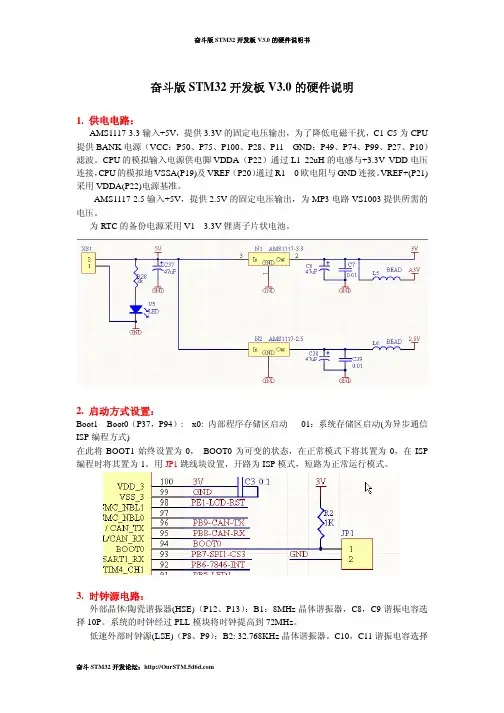
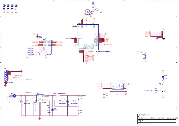
奋斗版STM32开发板V3.0的硬件说明1. 供电电路:AMS1117-3.3输入+5V,提供3.3V的固定电压输出,为了降低电磁干扰,C1-C5为CPU 提供BANK电源(VCC:P50、P75、P100、P28、P11 GND:P49、P74、P99、P27、P10)滤波。
CPU的模拟输入电源供电脚VDDA(P22)通过L1 22uH的电感与+3.3V VDD电压连接,CPU的模拟地VSSA(P19)及VREF-(P20)通过R1 0欧电阻与GND连接。
VREF+(P21)采用VDDA(P22)电源基准。
AMS1117-2.5输入+5V,提供2.5V的固定电压输出,为MP3电路VS1003提供所需的电压。
为RTC的备份电源采用V1 3.3V锂离子片状电池。
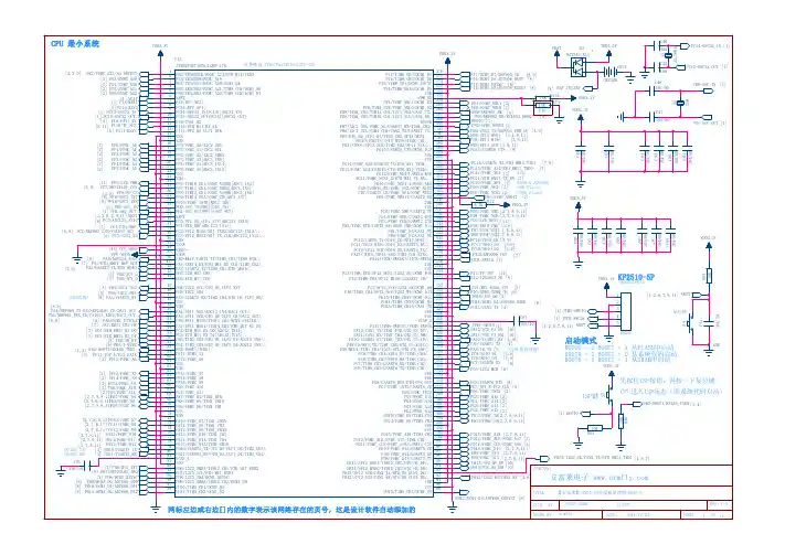
2. 启动方式设置:Boot1—Boot0(P37,P94): x0: 内部程序存储区启动01:系统存储区启动(为异步通信ISP编程方式)在此将BOOT1始终设置为0, BOOT0为可变的状态,在正常模式下将其置为0,在ISP 编程时将其置为1。
用JP1跳线块设置,开路为ISP模式,短路为正常运行模式。
3. 时钟源电路:外部晶体/陶瓷谐振器(HSE)(P12、P13):B1:8MHz晶体谐振器,C8,C9谐振电容选择10P。
系统的时钟经过PLL模块将时钟提高到72MHz。
低速外部时钟源(LSE)(P8、P9):B2: 32.768KHz晶体谐振器。
C10,C11谐振电容选择10P。
注意:根据ST公司的推荐, B2要采用电容负载为6P的晶振,否则有可能会出现停振的现象。
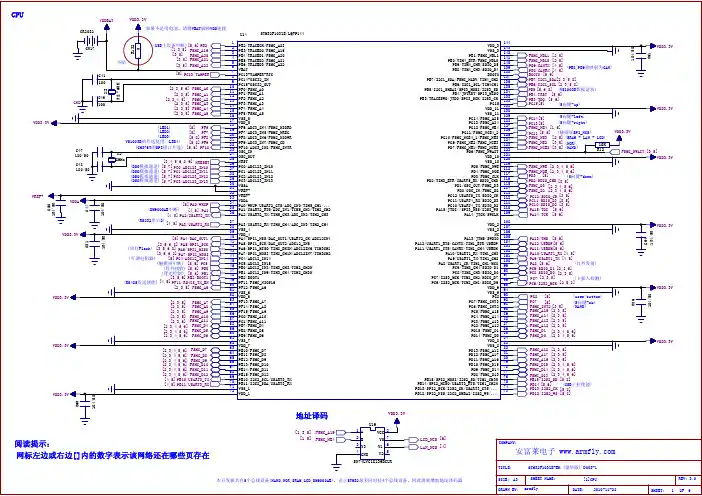
4. SPI存储电路:D2 SST25VF016B(2M Bytes)CPU采用SPI1端口PA7-SPI1-MOSI(P32)、PA6-SPI1-MISO (P31)、PA5-SPI1-SCK(P30)、PC4-SPI1-CS2(P33)控制读写访问, SPI1地址:0x4000 3800 - 0x4000 3BFF5. 显示及触摸接口模块:显示器采用2.4” TFT320X240LCD(控制器ILI9325), 采用CPU的FSMC功能,LCD片选CS采用FSMC_NE1(P88),FSMC_A16(P58)作为LCD的RS选择,FSMC_nWE(P86)作为LCD的/WR, FSMC_nOE(P85)作为LCD的/RD, LCD的RESET脚用CPU的PE1(P98)(LCD-RST),FSMC_D0---FSMC_D15和LCD的D1-D8 D10-D17相互连接,触摸屏接口采用SPI1接口,片选为PB7-SPI1-CS3,由于LCD背光采用恒流源芯片PT4101控制,采用了PWM控制信号控制背光的明暗, PWM信号由PD13-LIGHT-PWM来控制。
北京智嵌物联网电子技术ISTM32F107网络互联开发板3.0实验例程操作手册版本号:A拟制人:赵工时间:2013年7月1日目录1本文档编写目的 (1)2实验例程操作说明 (1)2.1LED闪烁实验 (1)2.2KEY_LED实验 (1)2.3RS232通讯实验 (1)2.4RS485通讯实验 (2)2.5CAN1通讯实验 (2)2.6CAN1与CAN2通讯实验 (3)2.7I2C实验—读写24c04 (4)2.8SPI通讯实验--读写SST2508B (5)2.9TCP服务器收发数据实验 (5)2.10动态IP实验 (7)2.11HTTP网页服务器实验 (7)2.12USB数据存储实验1(读写STM32F107片内flash) (9)2.13USB数据存储实验2(读写板载SST25F08B) (9)2.14U盘读写实验 (9)2.15USB鼠标实验 (11)2.16USB_JoyStickMouse实验 (11)2.17 2.4G无线模块NRF24l01通信实验 (12)2.18基于NRF24L01的无线RS232通讯实验 (12)2.19DS18B20温度试验 (13)2.20UDP客户端发送数据实验 (14)2.21UDP服务器收发数据实验 (15)2.22TCP客户端收发数据实验 (18)2.2316通道ADC采集实验 (21)2.24UDP与RS232RS485双向数据透明传输例程---开发板做服务器 (23)2.25TCP与RS232RS485双向数据透明传输实验 (23)2.26TCP与CAN双向数据透明传输实验 (23)1本文档编写目的本手册是针对STM32F107网络互联开发板V2.2的例程而编写的,包括每个实验例程的实验原理、实验步骤、注意事项等。
2实验例程操作说明2.1LED闪烁实验实验原理:通过控制PE2/PE3/PE4/PE5的电平变化实现LED灯的亮灭。
实验步骤:(1)用Keil uVision4打开LED灯闪烁实验工程,并编译。
stm32f103开发板原理图分析
1. 概述
文档适合STM32F103-EV AL开发板的用户使用,希望通过文档的描述可以使用户更快的进入产品的开发阶段。
2. 电路及接口说明
2.1. 电源模块
说明:
输入:5V DC
输出:3.3V DC
输出端接L1 会提高电源的质量。
2.2. 时钟供电模块说明:BT 为电池供电接口,板上有丝印标明正负极。
D3、D4 的作用是使板上供电和电池供电两种供电方式相互独立。
2.3. USB 通信模块
说明:开发板可以通过USB 接口供电,请不要同时使用USB 和外接电源供电。
D+为高时PC 认为有USB 设备接上并要求安装驱动程序,当只用USB 接口供电而不用USB 设备时JP7不接跳帽。
2.4. CAN 通信模块
说明:STB 接地为normal 模式,R34 不焊接。
2.5. RS232 通信模块
说明:D2、R29 为选择芯片的供电电源,板上D2 焊接,切勿两个器件同时焊接,否则5V 电源会灌到3.3V 供电电路上。
STM32F10x 的芯片的普通IO 可以接受5V 电平,可选择价格相对便宜的5V 供电的232芯片。
串口3 带CTS 和RTS 控制。
2.6. 红外通信模块
说明:红外接口与串口占用同一个串口,通过JP4、JP5 跳针来选择,跳针接1、2 脚选择RS232接口,调制接2、3 脚选择红外接口。
红外接口不焊接。
2.7. SPI 设。