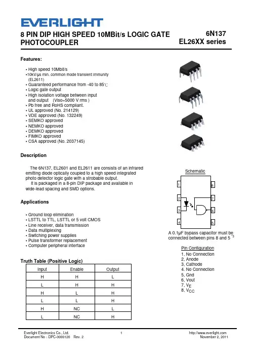
6N137数据手册
- 格式:pdf
- 大小:222.21 KB
- 文档页数:13
High Speed Optocoupler, 10 MBdVishay SemiconductorsDESCRIPTIONThe 6N137, VO2601 and VO2611 are single channel 10 Mbd optocouplers utilizing a high efficient input LED coupled with an integrated optical photodiode IC detector. The detector has an open drain NMOS-transistor output, providing less leakage compared to an open collector Schottky clamped transistor output. The VO2630, VO2631 and VO4661 are dual channel 10 MBd optocouplers. For the single channel type, an enable function on pin 7 allows the detector to be strobed. The internal shield provides a guaranteed common mode transient immunity of 5 kV/µs for the VO2601 and VO2631 and 15 kV/µs for the VO2611 and VO4661. The use of a 0.1 µF bypass capacitor connected between pin 5 and 8 is recommended.AGENCY APPROVALS•UL1577, file no. E52744 system code H or J, double protection•CUL - file no. E52744, equivalent to CSA bulletin 5A •DIN EN 60747-5-5 (VDE 0884) available with option 1•BSI IEC 60950FEATURES•Choice of CMR performance of 15 kV/µs,5 kV/µs, and 100 V/µs•High speed: 10 Mbd typical•+ 5 V CMOS compatibility•Pure tin leads•Guaranteed AC and DC performance over temperature: - 40 °C to + 100 °C temperature range •Meets IEC 60068-2-42 (SO2) and IEC 60068-2-43 (H2S) requirements•Low input current capability: 5 mA•Lead (Pb)-free component•Component in accordance to RoHS 2002/95/EC and WEEE 2002/96/ECAPPLICATIONS•Microprocessor system interface•PLC, ATE input/output isolation•Computer peripheral interface•Digital fieldbus isolation: CC-link, DeviceNet, profibus, SDS•High speed A/D and D/A conversion•AC plasma display panel level shifting•Multiplexed data transmission•Digital control power supply•Ground loop eliminationORDER INFORMATIONPART REMARKS6N137100 V/µs, single channel, DIP-86N137-X006100 V/µs, single channel, DIP-8 400 mil 6N137-X007100 V/µs, single channel, SMD-8 VO2601 5 kV/µs, single channel, DIP-8VO2601-X006 5 kV/µs, single channel, DIP-8 400 mil VO2601-X007 5 kV/µs, single channel, SMD-8 VO261115 kV/µs, single channel, DIP-8 VO2611-X00615 kV/µs, single channel, DIP-8 400 mil VO2611-X00715 kV/µs, single channel, SMD-8 VO2630100 V/µs, dual channel, DIP-8VO2630-X006100 V/µs, dual channel, DIP-8 400 mil VO2630-X007100 V/µs, dual channel, SMD-8VO2631 5 kV/µs, dual channel, DIP-8VO2631-X006 5 kV/µs, dual channel, DIP-8 400 milHigh Speed Optocoupler, 10 MBdVishay SemiconductorsNoteFor additional information on the available options refer to option information.Notes (1)T amb = 25°C, unless otherwise specified.Stresses in excess of the absolute maximum ratings can cause permanent damage to the device. Functional operation of the device is not implied at these or any other conditions in excess of those given in the operational sections of this document. Exposure to absolute maximum ratings for extended periods of the time can adversely affect reliability.(2)Refer to reflow profile for soldering conditions for surface mounted devices (SMD). Refer to wave profile for soldering conditions for through VO2631-X007 5 kV/µs, dual channel, SMD-8VO466115 kV/µs, dual channel, DIP-8VO4661-X00615 kV/µs, dual channel, DIP-8 400 mil VO4661-X00715 kV/µs, dual channel, SMD-8ORDER INFORMATIONPART REMARKSTRUTH TABLE (Positive Logic)LED ENABLEOUTPUTON H L OFF H H ON L H OFF L H ON NC L OFFNCHABSOLUTE MAXIMUM RATINGS (1)PARAMETER TEST CONDITIONSYMBOLVALUEUNITINPUTAverage forward current (single channel)I F 20mA Average forward current(per channel for dual channel)I F 15mA Reverse input voltage V R 5V Enable input voltage V E V CC + 0.5 VV Enable input current I E 5mA Surge currentt = 100 µsI FSM 200mA Output power dissipation (single channel)P diss 35mW Output power dissipation(per channel for dual channel)P diss25mWOUTPUT Supply voltage 1 min maximumV CC 7V Output current I O 50mA Output voltageV O 7V Output power dissipation (single channel)P diss 85mW Output power dissipation(per channel for dual channel)P diss60mWCOUPLERIsolation test voltage t = 1.0 sV ISO 5300V RMS Storage temperature T stg - 55 to + 150°C Operating temperature T amb- 40 to + 100°C Lead solder temperature for 10 s 260°C Solder reflow temperature (2)260°CVishay SemiconductorsHigh Speed Optocoupler, 10 MBdNoteT amb = 25 °C, unless otherwise specified.Minimum and maximum values are testing requirements. Typical values are characteristics of the device and are the result of engineering evaluation. Typical values are for information only and are not part of the testing requirements.RECOMMENDED OPERATING CONDITIONSPARAMETER TEST CONDITIONSYMBOL MIN.MAX.UNIT Operating temperature T amb - 40100°C Supply voltage V CC 4.5 5.5V Input current low level I FL 0250µA Input current high level I FH 515mA Logic high enable voltage V EH 2V CC V Logic low enable voltage V EL 00.8V Output pull up resistor R L 3304K ΩFanoutR L = 1 k ΩN5-ELECTRICAL CHARACTERISTICSPARAMETER TEST CONDITIONSYMBOLMIN.TYP.MAX.UNITINPUTInput forward voltage I F = 10 mA V F 1.11.4 1.7V Reverse current V R = 5 V I R 0.0110µA Input capacitance f = 1 MHz, V F = 0 VC I55pFOUTPUTHigh level supply current (single channel)V E = 0.5 V, I F = 0 mA I CCH 4.17.0mA V E = V CC , I F = 0 mAI CCH 3.3 6.0mA High level supply current (dual channel)I F = 0 mA I CCH 6.512.0mA Low level supply current (single channel)V E = 0.5 V, I F = 10 mA I CCL 4.07.0mA V E = V CC , I F = 10 mAI CCL 3.3 6.0mA Low level supply current (dual channel)I F = 10 mAI CCL 6.512.0mA High level output current V E = 2 V, V O = 5.5 V, I F = 250 µAI OH 0.0021µA Low level output voltage V E = 2 V, I F = 5 mA,I OL (sinking) = 13 mA V OL 0.20.6V Input threshold current V E = 2 V, V O = 5.5 V,I OL (sinking) = 13 mAI TH 2.4 5.0mA High level enable current V E = 2 V I EH - 0.6- 1.6mA Low level enable current V E = 0.5 VI EL - 0.8- 1.6mA High level enable voltage V EH 2V Low level enable voltageV EL0.8VHigh Speed Optocoupler, 10 MBdVishay SemiconductorsNotes(1)Over recommended temperature (T amb = - 40 °C to + 100 °C), V CC = 5 V, I F = 7.5 mA unless otherwise specified.All typicals at T amb = 25 °C, V CC = 5 V.(2)75 ns applies to the 6N137 only, a JEDEC registered specificationFig. 1 - Single Channel Test Circuit for t PLH , t PHL , t r and t fFig. 2 - Dual Channel Test Circuit for t PLH , t PHL , t r and t fSWITCHING CHARACTERISTICS (1)PARAMETERTEST CONDITION SYMBOL MIN.TYP.MAX.UNIT Propagation delay time to high output levelR L = 350 Ω, C L = 15 pF t PLH 204875 (2)ns t PLH 100ns Propagation delay time to low output levelR L = 350 Ω, C L = 15 pF t PHL 255075 (2)ns t PHL 100ns Pulse width disortion R L = 350 Ω, C L = 15 pF |t PHL - t PLH |2.935ns Propagation delay skew R L = 350 Ω, C L = 15 pF t PSK 840ns Output rise time (10 to 90 %)R L = 350 Ω, C L = 15 pF t r 23ns Output fall time (90 to 10 %)R L = 350 Ω, C L = 15 pF t f 7ns Propagation delay time of enable from V EH to V EL R L = 350 Ω, C L = 15 pF,V EL = 0 V, V EH = 3 V t ELH 12ns Propagation delay time of enable from V EL to V EHR L = 350 Ω, C L = 15 pF,V EL = 0 V, V EH = 3 Vt EHL11nsVishay SemiconductorsHigh Speed Optocoupler, 10 MBdFig. 3 - Single Channel Test Circuit for t EHL , and t ELHNotes(1)For 6N137 and VO2630(2)For VO2601 and VO2631(3)For VO2611 and VO4661Fig. 4 - Single Channel Test Circuit for Common Mode Transient ImmunityCOMMON MODE TRANSIENT IMMUNITYPARAMETERTEST CONDITIONSYMBOL MIN.TYP.MAX.UNIT Common mode transient immunity (high)|V CM | = 10 V, V CC = 5 V, I F = 0 mA,V O(min.) = 2 V, R L = 350 Ω, T amb = 25 °C (1)|CM H |100V/µs |V CM | = 50 V, V CC = 5 V, I F = 0 mA,V O(min.) = 2 V, R L = 350 Ω, T amb = 25 °C (2)|CM H |500010 000V/µs |V CM | = 1 kV, V CC = 5 V, I F = 0 mA,V O(min.) = 2 V, R L = 350 Ω, T amb = 25 °C (3)|CM H |15 00025 000V/µs |V CM | = 10 V, V CC = 5 V, I F = 7.5 mA,V O(max.) = 0.8 V, R L = 350 Ω, T amb = 25 °C (1)|CM L |100V/µs |V CM | = 50 V, V CC = 5 V, I F = 7.5 mA,V O(max.) = 0.8 V, R L = 350 Ω, T amb = 25 °C (2)|CM L |500010 000V/µs |V CM | = 1 kV, V CC = 5 V, I F = 7.5 mA,V O(max.) = 0.8 V, R L = 350 Ω, T amb = 25 °C (3)|CM L |15 00025 000V/µsHigh Speed Optocoupler, 10 MBdVishay SemiconductorsFig. 5 - Dual Channel Test Circuit for Common Mode Transient ImmunityNoteAs per IEC 60747-5-2, §7.4.3.8.1, this optocoupler is suitable for “safe electrical insulation” only within the safety ratings. Compliance with the safety ratings shall be ensured by means of prodective circuits.SAFETY AND INSULATION RATINGSPARAMETER TEST CONDITION SYMBOLMIN.TYP.MAX.UNITClimatic classification according to IEC 68 part 155/100/21Comparative tracking index CTI 175399Peak transient overvoltage V IOTM 8000V Peak insulation voltage V IORM 890V Safety rating - power output P SO 500mW Safety rating - input current I SI 300mA Safety rating - temperature T SI175°C Creepage distance standard DIP-87mm Clearance distance standard DIP-87mm Creepage distance 400 mil DIP-88mm Clearance distance400 mil DIP-88mm Insulation thickness, reinforced ratedper BSI 609500.2mmVishay Semiconductors High Speed Optocoupler, 10 MBd TYPICAL CHARACTERISTICST amb = 25 °C, unless otherwise specifiedFig. 6 - Forward Voltage vs. Ambient Temperature Fig. 7 - Forward Voltage vs. Forward Current Fig. 8 - Reverse Current vs. Ambient TemperatureFig. 9 - Low Level Supply Current vs. Ambient Temperature Fig. 10 - High Level Supply Current vs. Ambient Temperature Fig. 11 - Input Threshold On Current vs. Ambient TemperatureHigh Speed Optocoupler, 10 MBd Vishay SemiconductorsFig. 12 - Input Threshold Off Current vs. Ambient Temperature Fig. 13 - Low Level Output Voltage vs. Ambient Temperature Fig. 14 - Low Level Output Current vs. Ambient Temperature Fig. 15 - High Level Output Current vs. Ambient Temperature Fig. 16 - Output Voltage vs. Forward Input CurrentFig. 17 - Propagation Delay vs. Ambient TemperatureVishay Semiconductors High Speed Optocoupler, 10 MBdFig. 18 - Propagation Delay vs. Forward Current Fig. 19 - Pulse Width Distortion vs. Ambient Temperature Fig. 20 - Pulse Width Distortion vs. Forward CurrentFig. 21 - Rise and Fall Time vs. Ambient Temperature Fig. 22 - Rise and Fall Time vs. Forward CurrentFig. 23 - Enable Propagation Delay vs. Ambient TemperatureHigh Speed Optocoupler, 10 MBd Vishay Semiconductors PACKAGE DIMENSIONS in inches (millimeters) For technical questions, contact: optocoupler.answers@ Document Number: 84732184Rev. 1.3, 06-Oct-086N137, VO2601, VO2611, VO2630, VO2631, VO4661Vishay Semiconductors High Speed Optocoupler, 10 MBdOZONE DEPLETING SUBSTANCES POLICY STATEMENTIt is the policy of Vishay Semiconductor GmbH to1.Meet all present and future national and international statutory requirements.2.Regularly and continuously improve the performance of our products, processes, distribution and operating systems with respect to their impact on the health and safety of our employees and the public, as well as their impact on the environment.It is particular concern to control or eliminate releases of those substances into the atmosphere which are known as ozone depleting substances (ODSs).The Montreal Protocol (1987) and its London Amendments (1990) intend to severely restrict the use of ODSs and forbid their use within the next ten years. Various national and international initiatives are pressing for an earlier ban on these substances.Vishay Semiconductor GmbH has been able to use its policy of continuous improvements to eliminate the use of ODSs listed in the following documents.1.Annex A, B and list of transitional substances of the Montreal Protocol and the London Amendments respectively.2.Class I and II ozone depleting substances in the Clean Air Act Amendments of 1990 by the Environmental Protection Agency (EPA) in the USA.3.Council Decision 88/540/EEC and 91/690/EEC Annex A, B and C (transitional substances) respectively.Vishay Semiconductor GmbH can certify that our semiconductors are not manufactured with ozone depleting substances and do not contain such substances.We reserve the right to make changes to improve technical designand may do so without further notice.Parameters can vary in different applications. All operating parameters must be validated for each customer application by the customer. Should the buyer use Vishay Semiconductors products for any unintended or unauthorized application, the buyer shall indemnify Vishay Semiconductors against all claims, costs, damages, and expenses, arising out of, directly or indirectly, anyclaim of personal damage, injury or death associated with such unintended or unauthorized use.Vishay Semiconductor GmbH, P.O.B. 3535, D-74025 Heilbronn, GermanyDocument Number: 91000 Revision: 18-Jul-081DisclaimerLegal Disclaimer NoticeVishayAll product specifications and data are subject to change without notice.Vishay Intertechnology, Inc., its affiliates, agents, and employees, and all persons acting on its or their behalf (collectively, “Vishay”), disclaim any and all liability for any errors, inaccuracies or incompleteness contained herein or in any other disclosure relating to any product.Vishay disclaims any and all liability arising out of the use or application of any product described herein or of any information provided herein to the maximum extent permitted by law. The product specifications do not expand or otherwise modify Vishay’s terms and conditions of purchase, including but not limited to the warranty expressed therein, which apply to these products.No license, express or implied, by estoppel or otherwise, to any intellectual property rights is granted by this document or by any conduct of Vishay.The products shown herein are not designed for use in medical, life-saving, or life-sustaining applications unless otherwise expressly indicated. Customers using or selling Vishay products not expressly indicated for use in such applications do so entirely at their own risk and agree to fully indemnify Vishay for any damages arising or resulting from such use or sale. Please contact authorized Vishay personnel to obtain written terms and conditions regarding products designed for such applications.Product names and markings noted herein may be trademarks of their respective owners.This datasheet has been downloaded from:Free DownloadDaily Updated Database100% Free Datasheet Search Site100% Free IC Replacement Search SiteConvenient Electronic DictionaryFast Search SystemAll Datasheets Cannot Be Modified Without PermissionCopyright © Each Manufacturing Company。