AFE4361数据手册-1[1][1].0
- 格式:pdf
- 大小:411.05 KB
- 文档页数:7
PW4361E继电保护测试产品概述随着微机型继电保护装置的大量推广普及和对保护装置试验要求也不断的提高,传统的试验仪和试验方法已远远不能满足新型保护装置的需要。
微机技术的发展带来了全新的试验理念,使试验过程的智能化已成为发展的必然趋势。
PW4361E微机继电保护测试仪是我公司电力专家组和院校联手精心打造,技术性能符合GB/T7261-2000《继电器及装置基本试验方法》及DL/T624-1997《继电保护微机型试验装置技术条件》的要求,既可单机操作也可联接笔记本电脑运行,试验仪具有强大的功能,优秀的界面,独创旋转鼠标式操作取代传统的复杂的小键盘,只用一个旋钮完成全部数据的设置、修改或功能的切换。
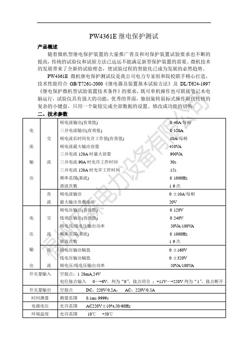
二、技术参数电流输出交流相电流输出(有效值) 0-40A/每相三并电流输出(有效值) 0-120A相电流长时间允许工作值(有效值) 10A/每相相电流最大输出容量450V A三并电流120A时最大容量900V A三并电流90A时允许工作时间30s三并电流120A时允许工作时间15s频率范围(基波) 0-1000Hz谐波次数1-9次直流相电流输出0-±10A/每相最大输出负载电压20V电压输出交流相电压输出(有效值) 0-120V线电压输出(有效值) 0-240V相电压/线电压输出功率50V A/100V A 频率范围(基波) 0-1000Hz谐波次数1-9次直流相电压输出幅值0-±160V线电压输出幅值0-±320V相电压/线电压输出功率50V A/100V A开关量输入空接点:1-20mA,24V电位接点输入0—+6V,判为“0”,接点闭合;+11V—+250V判为“1”,接点断开开关量输出空接点DC:220V/0.2A;AC:220V/0.5A时间测量测量范围0.1ms-9999s电源电压允许范围AC220V±10%,50/60Hz环境温度允许范围-10℃- +50℃额定范围内精度电流交流相电流<0.2%交流大电流端子输出<0.2%直流电流<0.2% 电压交流电压<0.2%直流电压<0.2% 其它频率精度(50Hz时) <0.01Hz相位精度<0.5O谐波失真度<0.5%时间测量精度<0.1ms三、装箱清单:PW4361E微机继电保护测试仪主机一台高强度铝合金主机包装箱一只测试导线一包电源线一根光电鼠标一个保险管一套四、外观参考图片:第二部分:质保及售后服务实施方案一、产品的质保◆本产品严格按照国家标准和企业标准制造,出厂前经过严格的检验。
BS-4361机组控制器说明书V1.00北京柏斯顿智能科技有限公司2017年2月目录1.产品介绍 (4)1.1产品功能 (4)1.2系统参数 (4)1.2.1开关量输入 (4)1.2.2PT100模拟量输入 (4)1.2.3通用模拟量输入 (4)1.2.4开关量输出 (5)1.2.5模拟量输出 (5)1.2.6电源 (5)1.2.7串口通讯 (5)1.3安装使用环境 (5)2.产品使用方法 (5)2.1通讯通道 (5)2.2拟量输入 (6)2.3开关量输入 (7)2.4开关量输出 (7)2.5模拟量输出 (7)2.6电源 (8)2.7连锁控制 (8)2.8回路调节 (9)2.9应用 (9)2.10系统参数设置 (9)2.10.1第一回路参数设置 (10)2.10.2第二回路参数设置 (11)2.10.3显示设置 (11)2.10.4量程及IO配置 (12)2.10.5调节回路配置 (13)2.10.6连锁回路配置 (14)2.10.7AI参数标定 (15)2.10.8输出及阀门位置标定 (17)2.10.9输入参数说明 (18)2.10.10通讯参数 (19)2.10.11密码设置 (20)2.11操作 (20)3.面板及接线端子 (23)4.MODBUS规约 (24)5.MODBUS数据分配 (25)6.外形及开孔尺寸 (27)BS-4361机组控制器说明书1.产品介绍BS-4361机组数字控制器(DDC)是我公司针对各种小型紧凑型空调应用场合,研发的专用于小规模完整的机组控制器,它尽量将小规模机组的各种控制集中在一台控制器重,并带有汉字操作界面(TFT),本控制器是一个柜(盘)面嵌装仪表,机组的启动/停止、参数的控制操作和信息的指示都集中于仪表的TFT面板上。
本控制器使用于空调行业的新风机组,空调机组及加热器/换热器等须多种信号混合控制的场合。
1.1产品功能●2寸TFT显示器,176X220点阵,16位真彩色,最大11行汉字。
Single and Dual Input Analyzersfor High-level ConductivityAX430, AX433, AX413 and AX436■ Cost effective– select one or two Conductivity inputs or combine pH/Redox (ORP) with Conductivity in one analyzer –integral PID controller (AX430)■ Advanced measuring capabilities– conductivity range up to 1,999 mS cm –1– selectable concentration ranges:0 to 15% NaOH, 0 to 18% HCl, 0 to 20% H 2SO 4,0 to 40% H 3PO 4, 0 to 20% NaCl and user-defined ■ Dosing Control functionality – long dose diagnostic alarm – initial charge function■ Reduced installation cost– easy access terminations; reduced panel space ■ High functionality at minimum cost– three alarms and two fully-isolated current outputs – direct linear, reverse acting or bi-linear output ■ Expanded monitoring and control– add-on option board provides a total of five alarm relays and four current outputs– service logbook providing historical data ■ Reduced yearly maintenance costs– 12 to 30V DC option negates the need for costly safety tests ■ Wide range of applicability – regeneration of ion exchangers– municipal water phosphoric acid control– food & beverage product/water interface detection – clean-in-place concentration monitoringMore processing power,higher performanceData SheetSS/AX4CO4_5Single and Dual Input Analyzers for High-level Conductivity AX430, AX433, AX413 and AX436SS/AX4CO4_52The AX400 SeriesAX400 analyzers incorporate the latest technology to provide highly reliable, flexible, feature-packed devices that satisfy a diverse range of process monitoring and control applications.The complete range encompasses solutions for pH/Redox (ORP), conductivity and dissolved oxygen.AX43x analyzers enable continuous measurements of one or two conductivity points with simultaneous local display and retransmission. AX43x is used with the TB4 and AC400* Series of insertion, immersion and flow-through, four-electrode conductivity cells providing measurements with exceptional accuracy and performance.AX400 Series analyzers are available for either wall-/pipe- or panel-mounting and are rated to IP66/NEMA 4X.* Check with factory for availability.High Functionality as StandardAll versions are supplied with two, fully-isolated current outputs as standard, that can be assigned to the measured parameter,sample temperature or any appropriate calculated variables.Three programmable relay set points are available which can also be assigned as required.Innovative features such as a power saving display and a diagnostic current output option all contribute to a low cost of ownership.Plug-and-Produce Expanded ControlAn advanced function card provides an additional two current outputs and two further alarm relays that can be assigned to either measured values or sample temperature.ABB Plug-and-Produce software automatically reconfigures the analyzer if an option board is added later. No user programming is necessary.A real-time clock and logbook are also included making the full-facility versions extremely powerful and versatile.Significantly Reduced Maintenance CostsThe AX400 Analyzers are supplied as standard for 85 to 265V AC operation. There are no inner switches to set.They can also be provided for 24V AC, or 12 to 30V DC, supply and recognize automatically which of the two supplies is being used. 24V DC operation reduces maintenance costs significantly by negating the need for costly, yearly safety tests to ensure compliance with safety procedures.Energy Saving DisplayThe backlit display has been designed to operate in all types of environments and shows both the measured parameter(s) and,on a separate 16-character display line, diagnostic and computed information.On dual-input analyzers both measured parameters are displayed simultaneously.For conservation of energy, the backlight can be set to switch off automatically after 60s of inactivity.Backlight Can be Set to Switch-off When InactiveEasy Access Installation TerminalsE asy access to the terminations ensures rapid and cost-effective installation. The wall-/pipe-mount version has been designed to ensure that cable connection is simple and convenient. Ingress protection of the electronics section is retained even when the terminal compartment is opened.AX400 Termination Chamber Makes Access EasyAX400 OutputsSingle and Dual Input Analyzers for High-level Conductivity AX430, AX433, AX413 and AX436SS/AX4CO4_53Advanced Conductivity and Concentration MonitoringIn addition, these analyzers enable operation directly in terms of concentration: 0 to 15% NaOH, 18% HCl, 20% H 2SO 4,40% H 3PO 4, 20% NaCl and user-defined. This is particularly suited for strength-monitoring of ion exchange regenerant acid and alkali.Cost-effective Control of CIP PlantAX43x conductivity analyzers measure up to 1,999mS cm –1enabling operation in the majority of high concentration processes. Automatic and manual temperature compensations enable effective measurements up to 300°C (572°F).Single and Dual Input Analyzers for High-level Conductivity AX430, AX433, AX413 and AX436SS/AX4CO4_54AX436 Combined Conductivity and pHThe AX436 version measures conductivity and pH with the same analyzer. The option board provides the capability to retransmit conductivity, pH and both sample temperatures. This is particularly useful in the paper industry, reducing the investment in separate instruments, for example, when used on white water or the head box.Simultaneous Conductivity and pH MeasurementDual Input MeasurementSingle and Dual Input Analyzers for High-level Conductivity AX430, AX433, AX413 and AX436SS/AX4CO4_55Long-dose Alarm FunctionAn important diagnostic capability incorporated in AX43x analyzers is the long-dose alarm function. This is useful for occasions when faults occur in the dosing system.The analyzers can be configured to provide an alarm if a set point has not been reached within a specified time. This valuable facility provides a warning that could indicate a loss of dosing chemicals, a leakage or a costly pump failure.Long-dose Alarms Warns of Dosing Systems FaultsInitial Charge FunctionIn some applications, fresh dosing chemical reagent is made up every few days. For example, in bottle-washing plants the caustic solution can become dirty and must be replaced regularly. In the case of a new charge, i.e. making up a fresh reagent dilution, a general long-dose alarm could be initiated before the reagent had attained the correct concentration.AX43x analyzers provide a simple solution by having a pre-configurable Initial Charge function. A simple button press from Initial Charge Function When Making Fresh ReagentSingle and Dual Input Analyzers for High-level Conductivity AX430, AX433, AX413 and AX436SS/AX4CO4_56AX430 Integral P, PI and PID ControlThe single input AX430 analyzers incorporate three-term PID Control, offering three modes of sophisticated control: analog,pulse length (time proportional) and pulse frequency. These are supplied as standard and can be operated in direct- or reverse-acting mode, depending upon the application.Auto/Manual and Bumpless TransferAn auto/manual feature is incorporated for rapid manual access to the control functions. The controller facilitates bumpless transfer between manual and auto modes, providing the measured variable is within the proportional band and some integral action time has been programmed.Current Output Proportional ControlIn this case, the control signal is provided by the 4 to 20mA output of AX430 analyzers rather than using the alarm/control contacts. The magnitude of the current output changes in proportion to the deviation from set point. This method is used generally with motorized valves or when controlling the speed of dosing pumps with a 4 to 20mA proportional input.Pulse-frequency Proportional ControlImpulse pumps dosing chemical reagents are controlled easily by the AX430 analyzer’s pulse-frequency proportional control output. In this case, the pulse length of the alarm/control contact is fixed and the frequency of the delivered pulses increases in proportion to the system error, as set by the proportional band.Diaphragm metering pumps must have a remote pulse input capability in order to utilize this function.Pulse-frequency control in the AX430 analyzer operates by pulsing a relay on for 300ms and off for a period of time determined by the pulse frequency. The pulse frequency (PFr) is adjustable between 1 and 120 pulses per minute. The greater the difference between the measured variable and the set point,the greater the pulse frequency.ExampleIf the pulse frequency is set at 120 pulses per minute and the percentage output is 100% then the pulse rate is 2 pulses per second. If the percentage output is reduced to 50%, the pulse rate falls to one pulse per second.Pulse-frequency Proportional ControlPower Failure RecoveryIn the event of a power failure the user can configure the control mode to be Auto, Manual or Last. This optimizes control conditions on power-up to ensure rapid recovery of process control.Time Proportioning ControlOutput = 0%Output = 50%Output = 100%Energized De-energized EnergizedDe-energizedPermanently De-energized Pulse Frequency = 120 pulses per minute0.3s 0.7ms0.3s 0.2s 0.3s 0.2sSingle and Dual Input Analyzers for High-level Conductivity AX430, AX433, AX413 and AX436SS/AX4CO4_57SpecificationConductivityRangeConductivity Programmable 0.000 to 1999mScm –1(uncompensated)Concentration0.000 to 1.999 digits (user configurable)Selectable concentration ranges 0 to 15% NaOH0 to 18% HCl 0 to 20%H 2SO 40 to 40% H 3PO 40 to 20% NaCl User-defined table Temperature–20 to 300°C (–4 to 572°F )Sensor Full Scale Measurement Ranges(a) TB4 Group A and AC400 cells 0 to 1,999mS cm –1(uncompensated)(b) TB4 Group B cells 0 to 1,999μS cm –1(uncompensated)Minimum span (a)TB4 Group A and AC400 cells 100.0μS cm –1(b)TB4 Group B cells 10.00μS cm –1Concentration 5% of the maximum set concentration range Temperature10°C (50°F)Note . Refer to corresponding data sheets for process limit specifications of TB4 and AC400 cells.Resolution, Display Conductivity(a)TB4 Group A cells 0.1 μS cm –1AC400 cells 0.1mS cm –1(b)TB4 Group B cells 0.01μS cm–1Concentration 0.001 digits(configuration dependent)Temperature 0.1°C (0.1°F)Accuracy, Display Conductivity ± 0.5% measurement range per decade Temperature10°C (21°F)Display temperature range –20 to 300°C (4 to 572°F)Temperature sensor Pt1000 or 3k BalcoTemperature coefficientProgrammable 0 to 9.99%/°C and fixed temperaturecompensation curves (programmable) for acids and neutral salt Reference temperature 25°C (77°F)Dosing control functions Long-dose alarm 0 to 10 mins. (user-configurable)Initial charge function0 to 30 mins. (user-configurable)DisplayTypeDual 5-digit, 7-segment backlit LCD Information16-character, single line dot-matrixEnergy-saving functionBacklit LCD configurable as ON or Auto-Off after 60sLogbook*Electronic record of major process events and calibration data Real-time clock*Records time for logbook and auto-manual functions *Available if option board is fitted Retransmission outputs2 (4 optional) fully-isolated standardRelay Outputs – On/OffNumber of relaysThree, supplied as standardFive, when ordered with option boardNumber of set points3 supplied as standard or 5 with option card fittedSet point adjustmentConfigurable as normal or failsafe high/low, bandwidth alarm (composite high/low) or diagnostic alert Hysteresis of readingProgrammable 0 to 5% in 0.1% increments DelayProgrammable 0 to 60s in 1s intervals Relay contactsSingle-pole changeover Rating 5A, 115/230V AC, 5A DC Insulation2kV RMS contacts to earth/groundAnalog OutputsNumber of current outputs (fully isolated)Two supplied as standard or 4 with option board fitted Output ranges0 to 10mA, 0 to 20mA or 4 to 20mAAnalog output programmable to any value between 0 and 22mA to indicate system failureAccuracy±0.25% FSD, ±0.5% of reading (whichever is the greater)Resolution0.1% at 10mA, 0.05% at 20mASingle and Dual Input Analyzers for High-level Conductivity AX430, AX433, AX413 and AX436SS/AX4CO4_58…Specification…Analog OutputsMaximum load resistance 750Ω at 20mAConfigurationCan be assigned to either measured variable or either sample temperatureDigital CommunicationsCommunicationsProfibus DP (with option board fitted)Control Function – AX430 OnlyController TypeP, PI, PID (Configurable)Control OutputsAnalogCurrent output control (0 to 100%)Time proportioning cycle time1.0 to 300.0s, programmable in increments of 0.1s Pulse frequency1 to 120 pulses per minute, programmable in increments of 1 pulse per minute Controller action Direct or reverseProportional band0.1 to 999.9%, programmable in increments of 0.1%Integral action time (Integral reset)1 to 7200s, programmable in increments of 1s (0 = Off)Derivative0.1 to 999.9s in increments of 0.1s,available only for single set point control Auto/ManualUser-programmableAccess to FunctionsDirect keypad accessMeasurement, maintenance, configuration,diagnostics or service functionsPerformed without external equipment or internal jumpersMechanical DataWall-/Pipe-mount versions IP66/NEMA4XDimensions 192mm high x 230mm wide x 94mm deep (7.56 in. high x 9.06 in. wide x 3.7 in. deep)Weight 1kg (2.2 lb)Cable Entry Types Standard 5 or 7 x M20 cable glands N. American7 x knockouts suitable for 1/2 in. Hubble glandPanel-mount versions IP66/NEMA4X (front only)Dimensions 96mm x 96mm x 162mm deep (3.78 in. x 3.78 in. x 6.38 in. deep)Weight 0.6kg (1.32 lb)Power SupplyVoltage requirements 85 to 265V AC 50/60 Hz24V AC or 12 to 30V DC (optional)Power consumption <10VAInsulationMains to earth (line to ground) 2kV RMSEnvironmental DataOperating temperature limits –20 to 65°C (–4 to 149°F)Storage temperature limits –25 to 75°C (–13 to 167°F)Operating humidity limitsUp to 95%RH non condensingEMCEmissions and immunity Meets requirements of:EN61326 (for an industrial environment)EN50081-2EN50082-2Hazardous area approvalsCENELEC ATEX IIG EEx n IIC T4Pending FM non-incendive Class I Div. 2 Groups A to D Pending CSA non-incendive Class I Div. 2 Groups A to DPendingSafetyGeneral safety EN61010-1Overvoltage Class II on inputs and outputs Pollution category 2LanguagesLanguages configurable:English Italian French SpanishGermanSingle and Dual Input Analyzers for High-level ConductivityAX430, AX433, AX413 and AX436SS/AX4CO4_5 Overall Dimensions9Single and Dual Input Analyzers for High-level ConductivityAX430, AX433, AX413 and AX436SS/AX4CO4_5 Electrical Connections10Single and Dual Input Analyzers for High-level Conductivity AX430, AX433, AX413 and AX436SS/AX4CO4_511Ordering Information4X A .g .e ,1V P r o f t i g i d e d o c e h t 614X A ,e l b i s s i m r e p 16.e l b i s s i m r e p t o n **.)2V P (e l b a i r a V s s e c o r P d n o c e S s a d e t c e l e s s i m c /S m 999,1o t 0n e h w g n i s u o h t n u o m -l e n a p n i e l b a l i a v a t o n P D s u b if o r P †.n o i t a z i l a c i p o r t f o y t i l i b a l i a v a r o f y r o t c a f k c e h CSingle and Dual Input Analyzers for High-level Conductivity AX430, AX433, AX413 and AX436SS/AX4CO4_5S S /A X 4C O 4I s s u e 5ABB LimitedOldends Lane, Stonehouse Gloucestershire GL10 3TA UKTel:+44 (0)1453 826661Fax:+44 (0)1453 829671ABB Inc.Analytical Instruments9716 S. Virginia St. Ste., E Reno, Nevada 89521USATel:+1 775 850 4800Fax:+1 775 850 4808ABB has Sales & Customer Supportexpertise in over 100 countries worldwide The Company’s policy is one of continuous product improvement and the right is reserved to modify theinformation contained herein without notice.Printed in UK (08.05)© ABB 2005。
1436112fT YPICAL APPLICATIOND ESCRIPTION Protection ControllerA PPLICATIONS nUSB Protection n Handheld Computers n Cell/Smart Phones n MP3/MP4 Players n Digital Camerasn2.5V to 5.5V Operationn Overvoltage Protection Up to 80Vn No Input Capacitor or TVS Required for Most Applicationsn 2% Accurate 5.8V Overvoltage Thresholdn 10% Accurate 50mV Overcurrent Circuit Breaker n <1μs Overvoltage Turn-Off, Gentle Shutdown n Controls N-Channel MOSFETn Adjustable Power-Up dV/dt Limits Inrush Current n Reverse Voltage Protection n Power Good Output n Low Current Shutdownn Latchoff (L TC4361-1) or Auto-Retry (L TC4361-2) After Overcurrentn Available in 8-Lead ThinSOT™ and 8-Lead (2mm × 2mm) DFN PackagesThe L TC ®4361 overvoltage/overcurrent protection control-ler safeguards 2.5V to 5.5V systems from input supply overvoltage. It is designed for portable devices with multiple power supply options including wall adaptors, car battery adaptors and USB ports.The L TC4361 controls an external N-channel MOSFET in series with the input power supply. During overvoltage transients, the L TC4361 turns off the MOSF ET within 1μs, isolating downstream components from the input supply. Inductive cable transients are absorbed by the MOSFET and load capacitance. In most applications, the L TC4361 provides protection from transients up to 80V without requiring transient voltage suppressors or other external components.The L TC4361 has a delayed start-up and adjustable dV/dt ramp-up for inrush current limiting. A PWRGD pin provides power good monitoring for V IN . The L TC4361 features a soft shutdown controlled by the ON pin and drives an optional external P-channel MOSF ET for negative voltage protection. F ollowing an overvoltage condition, the L TC4361 automati-cally restarts with a start-up delay. After an overcurrent fault, the L TC4361-1 remains off while the L TC4361-2 automatically restarts after a 130ms start-up delay.L , L T , L TC, L TM, Linear Technology and the Linear logo are registered trademarks and ThinSOT , Hot Swap, No R SENSE and PowerPath are trademarks of Linear Technology Corporation. All other trademarks are the property of their respective owners.Output Protected from Overvoltage at InputProtection from Overvoltage and OvercurrentOUT V V GATE 10V/DIVV IN , V OUT 5V/DIV 0.5μs/DIV436112 TA01bSi1470DH C OUT = 10μFV OUTV INFEATURES2436112fBias Supply Voltage (IN) ............................–0.3V to 85V Input VoltagesSENSE ...................................................–0.3V to 85V OUT, ON ...................................................–0.3V to 9V Output Voltages PWRGD ....................................................–0.3V to 9V GATE (Note 3) ........................................–0.3V to 15V GATEP ....................................................–0.3V to 85V IN to GATEP ...........................................–0.3V to 10V(Notes 1, 2)ORDER INFORMATIONLead Free FinishTAPE AND REEL (MINI)TAPE AND REEL PART MARKING*PACKAGE DESCRIPTION TEMPERATURE RANGE L TC4361CTS8-1#TRMPBF L TC4361CTS8-1#TRPBF L TDWN 8-Lead Plastic TSOT-230°C to 70°C L TC4361CTS8-2#TRMPBF L TC4361CTS8-2#TRPBF L TFMN 8-Lead Plastic TSOT-230°C to 70°C L TC4361ITS8-1#TRMPBF L TC4361ITS8-1#TRPBF L TDWN 8-Lead Plastic TSOT-23–40°C to 85°C L TC4361ITS8-2#TRMPBF L TC4361ITS8-2#TRPBF L TFMN 8-Lead Plastic TSOT-23–40°C to 85°C L TC4361CDC-1#TRMPBF L TC4361CDC-1#TRPBF LDWP 8-Lead (2mm × 2mm) Plastic DFN 0°C to 70°C L TC4361CDC-2#TRMPBF L TC4361CDC-2#TRPBF LFMP 8-Lead (2mm × 2mm) Plastic DFN 0°C to 70°C L TC4361IDC-1#TRMPBF L TC4361IDC-1#TRPBF LDWP 8-Lead (2mm × 2mm) Plastic DFN –40°C to 85°C L TC4361IDC-2#TRMPBFL TC4361IDC-2#TRPBFLFMP8-Lead (2mm × 2mm) Plastic DFN–40°C to 85°CTRM = 500 pieces. *Temperature grades are identifi ed by a label on the shipping container .Consult L TC Marketing for parts specifi ed with wider operating temperature ranges.Consult L TC Marketing for information on lead based fi nish parts.For more information on lead free part marking, go to: http://www.linear .com/leadfree/For more information on tape and reel specifi cations, go to: http://www.linear .com/tapeandreel/A BSOLUTE MAXIMUM RATINGSP IN CONFIGURATION Operating Temperature RangeLTC4361C ................................................0°C to 70°C LTC4361I .............................................–40°C to 85°C Storage Temperature Range ..................–65°C to 150°C Lead Temperature (Soldering, 10 sec) TSOT .................................................................300°CON 1OUT 2GATEP 3GND 48PWRGD 7 GATE 6 SENSE 5 INTOP VIEWTS8 PACKAGE8-LEAD PLASTIC TSOT-23T JMAX = 125°C, θJA = 195°C/WTOP VIEWGND GATEP OUT ON IN SENSE GATE PWRGDDC PACKAGE8-LEAD (2mm s 2mm) PLASTIC DFN941236578T JMAX = 125°C, θJA = 102°C/WEXPOSED PAD (PIN 9) IS GND, CONNECTION OPTIONAL3436112fE LECTRICAL CHARACTERISTICS Note 1: Stresses beyond those listed under Absolute Maximum Ratings may cause permanent damage to the device. Exposure to any Absolute Maximum Rating condition for extended periods may affect device reliability and lifetime.Note 2: All currents into device pins are positive; all currents out of device pins are negative. All voltages are referenced to GND unless otherwise specifi ed.The l denotes the specifi cations which apply over the full operatingtemperature range, otherwise specifi cations are at T A = 25°C. V IN = 5V , V ON = 0V , unless otherwise noted.SYMBOL PARAMETER CONDITIONSMIN TYP MAX UNITSSupplies V IN Input Voltage Range l 2.580V V IN(UVL)Input Undervoltage Lockout V IN Rising l 1.82.1 2.45V I INInput Supply CurrentV ON = 0V l 220400μA V ON = 2.5Vl1.510μA Thresholds V IN(OV)IN Pin Overvoltage Threshold V IN Rising l 5.684 5.8 5.916V ΔV OV Overvoltage Hysteresis l 25100200mV ΔV OC Overcurrent ThresholdV IN – V SENSEl 455055mV External Gate DriveΔV GATE External N-Channel MOSFET Gate Drive (V GATE – V OUT )2.5V ≤ V IN < 3V , I GATE = –1μA 3V ≤ V IN < 5.5V , I GATE = –1μAl l 3.54.5 4.5667.9V V V GATE(TH)GATE High Threshold for PWRGD Status V IN = 3.3VV IN = 5V l l 5.76.7 6.37.2 6.87.8V V I GATE(UP)GATE Pull-Up Current V GATE = 1V l –5–10–15μA V GATE(UP)GATE Ramp-Up V GATE = 1V to 7Vl 1.53 4.5V/ms I GATE(FST)GATE Pull-Down Current Fast Turn-Off, V IN = 6V , V GATE = 9V l 153060mA I GATE(DN)GATE Pull-Down Current V ON = 2.5V , V GATE = 9V l 104080μA Input Pins I OUT(IN)OUT Input Current V OUT = 5V , V ON = 0V V OUT = 5V , V ON = 2.5Vl l 510020±3μA μA V ON (TH)ON Input Threshold l 0.4 1.5V I ONON Pull-Down Current V ON = 2.5V l2.5510μA Output Pins V GATEP(CLP)IN to GATEP Clamp Voltage l 5 5.87.5V R GATEP GATEP Resistive Pull-Down V GATEP = 3Vl 0.82 3.2MΩV PWRGD (OL)PWRGD Output Low Voltage V IN = 5V , I PWRGD = 3mA l 0.230.4V R PWRGD PWRGD Pull-Up Resistance to OUTV IN = 6.5V , V PWRGD = 1V l250500800kΩDelay t ON GATE On DelayV IN High to I GATE = –5μAl 50130200ms t OFF GATE Off Propagation Delay V IN = Step 5V to 6.5VV IN – V SENSE = Step 0mV to 100mV l l 50.2510120μs μs t PWRGD PWRGD Delay V IN = Step 5V to 6.5VV GATE > V GATE(TH) to PWRGD Low l l 250.25651100μs ms t ON (OFF)ON High to GATE OffV ON = Step 0V to 2.5Vl25μsNote 3: An internal clamp limits V GATE to a minimum of 4.5V above V OUT .Driving this pin to voltages beyond this clamp may damage the device.4436112fT YPICAL PERFORMANCE CHARACTERISTICS PWRGD Voltage vs PWRGD CurrentGATE Off Propagation Delay vs OverdriveNormal Start-Up SequenceGATE Slow Ramp-UpEntering Sleep ModeInput Supply Currentvs Input VoltageGATE Drive vs GATE CurrentGATE Fast Pull-Down Current vs TemperatureV IN (V)10.1I I N (μA )1100100010000100436112 G011010I GATE (μA)00$V G A T E (V )4321678481012436112 G02526TEMPERATURE (°C)–5020I G A T E (F S T ) (m A )25303540–2502550436112 G0375100I PWRGD (mA)00V P W R G D (O L ) (mV )2001003004005001234436112 G045V OVDRV (V)t O F F (μs )165432780.51 1.52436012 G052.5V IN 5V/DIV V GATE 10V/DIV V OUT 5V/DIVI CABLE 0.5A/DIV20ms/DIV436112 G07FIGURE 5 CIRCUITR IN = 150mΩ, L IN = 0.7μH R SENSE = 25mΩLOAD = 10Ω, C OUT = 10μFV IN 5V/DIV V GATE 10V/DIV V OUT 5V/DIVI CABLE 0.5A/DIV1ms/DIV436112 G08FIGURE 5 CIRCUITR IN = 150mΩ, L IN = 0.7μH R SENSE = 25mΩLOAD = 10Ω, C OUT = 10μFV ON 5V/DIV V GATE 10V/DIVV OUT 5V/DIVI CABLE 0.5A/DIV50μs/DIV436112 G09FIGURE 5 CIRCUITR IN = 150mΩ, L IN = 0.7μH R SENSE = 25mΩLOAD = 10Ω, C OUT = 10μFT A = 25°C, V IN = 5V , V ON = 0V , unless otherwise noted.V IN (V)2.54V G A T E /V G G A T E (T H ) (V )658 3.54354.5436112 G065.5101279116GATE Voltage and GATE High Threshold (for PWRGD Status) vs Input VoltageP IN FUNCTIONSExposed Pad (DFN): Ground. Connection to PCB is optional.GATE: Gate Drive for External N-Channel MOSF ET. An internal charge pump provides a 10μA pull-up current to charge the gate of the external N-channel MOSFET. An additional ramp circuit limits the GATE ramp rate when turning on to 3V/ms. For slower ramp rates, connect an external capacitor from GATE to GND. An internal clamp limits GATE to 6V above the OUT pin voltage. An internal GATE high comparator controls the PWRGD pin. GATEP: Gate Drive for External P-Channel MOSFET. GATEP connects to the gate of an optional external P-channel MOSFET to protect against negative voltages at IN. This pin is internally clamped to 5.8V below V IN. An internal 2M resistor connects this pin to ground. Connect to IN if not used.GND: Device Ground.IN: Supply Voltage Input. Connect this pin to the input power supply. This pin has an overvoltage threshold of 5.8V. After an overvoltage event, this pin must fall below V IN(OV) – ΔV OV to release the overvoltage lockout. Dur-ing lockout, GATE is held low and the PWRGD pull-down releases.ON: On Control Input. A logic low at ON enables theL TC4361. A logic high at ON activates a low current pull-down at the GATE pin and causes the L TC4361 to entera low current sleep mode. An internal 5μA current pulls ON down to ground. Connect to ground or leave open ifunused.OUT: Output Voltage Sense Input for GATE Clamp. Connectto the source of the external N-channel MOSFET to sensethe output voltage for GATE to OUT clamp. PWRGD: Power Good Status. Open-drain output with internal 500k resistive pull-up to OUT. Pulls low 65ms after GATE ramps above V GATE(TH).SENSE: Current Sense Input. Connect a sense resistorbetween IN and SENSE. An overcurrent protection circuitturns off the N-channel MOSFET when the voltage acrossthe sense resistor exceeds 50mV for more than 10μs.5436112fB LOCK DIAGRAM6436112fO PERATIONMobile devices like cell phones and MP3/MP4 players have highly integrated subsystems fabricated from deep submi-cron CMOS processes. The small form factor is accompanied by low absolute maximum voltage ratings. The sensitive electronics are susceptible to damage from transient or DC overvoltage conditions from the power supply. Failures or faults in the power adaptor can cause an over-voltage event. So can hot-plugging an AC adaptor into the power input of the mobile device (see L TC Application Note 88). Today’s mobile devices derive their power supply or recharge their internal batteries from multiple alternative inputs like AC wall adaptors, car battery adaptors and USB ports. A user may unknowingly plug in the wrong adaptor, damaging the device with a high or even a negative power supply voltage.The L TC4361 protects low voltage electronics from these overvoltage conditions by controlling a low cost external N-channel MOSFET confi gured as a pass transistor. At power-up (V IN > 2.1V), a start-up delay cycle begins. Any overvoltage condition causes the delay cycle to continue until a safe voltage is present. When the delay cycle completes, an internal high side switch driver slowly ramps up the MOSFET gate, powering up the output at a controlled rate and limiting the inrush current to the output capacitor. If the voltage at the IN pin exceeds 5.8V (V IN(OV)), GATE is pulled low quickly to protect the load. The incoming power supply must remain below 5.7V (V IN(OV) – ΔV OV) for the duration of the start-up delay to restart the GATE ramp-up.A sense resistor placed between IN and SENSE implements an overcurrent protection with a 50mV trip threshold and a 10μs glitch fi lter. After an overcurrent, the L TC4361-1 latches off while the L TC4361-2 restarts following a 130ms delay.The L TC4361 has a CMOS compatible ON input. When driven low, the part is enabled. When driven high, the external N-channel MOSFET is turned off and the supply current of the L TC4361 drops to 1.5μA. The PWRGD pull-down releases during this low current sleep mode, UVLO, overvoltage or overcurrent and the subsequent 130ms start-up delay. After the start-up delay, GATE starts its slow ramp-up and ramps higher than V GATE(TH) to trigger a 65ms delay cycle. When that completes, PWRGD pulls low.The L TC4361 has a GATEP pin that drives an optional external P-channel MOSFET to provide protection against negative voltages at IN.7436112f8436112fThe typical L TC4361 application protects 2.5V to 5.5V systems in portable devices from power supply overvolt-age. The basic application circuit is shown in Figure 1. Device operation and external component selection is discussed in detail in the following sections.APPLICATIONS INFORMATIONFigure 1. Protection from Input Overvoltage and OvercurrentM1R SENSE OUT V IN 5VThe GATE ramp rate is limited to 3V/ms. V OUT follows at a similar rate which results in an inrush current into the load capacitor C OUT of:I INRUSH =C OUT •dV GATEdt=C OUT •3 mA/µF []The servo loop is compensated by the parasitic capaci-tance of the external MOSFET . No further compensation components are normally required. In the case where the parasitic capacitance is less than 100pF, a 100pF compensation capacitor between GATE and ground may be required.An even slower GATE ramp and lower inrush current can be achieved by connecting an external capacitor , C G , from GATE to ground. The voltage at GATE then ramps up with a slope equal to 10μA/C G [V/s]. Choose C G using the formula:C G =10µA I INRUSH •C OUTOvervoltageWhen power is fi rst applied, V IN must remain below 5.7V(V IN(OV) – ΔV OV ) for more than 130ms before GATE is ramped up to turn on the MOSFET . If V IN then rises above 5.8V (V IN(OV)), the overvoltage comparator activates the 30mA fast pull-down on GATE within 1μs. After an over-voltage condition, the MOSFET is held off until V IN once again remains below 5.7V for 130ms.OvercurrentThe overcurrent comparator protects the MOSFET from excessive current. It trips when the SENSE pin falls more than 50mV below IN for more than 10μs. When the overcur-rent comparator trips, GATE is pulled low quickly and the PWRGD pull-down releases. The L TC4361-2 automatically tries to apply power again after a 130ms start-up delay.Start-UpWhen V IN is less than the undervoltage lockout level of 2.1V , the GATE driver is held low and the PWRGD pull-down is high impedance. When V IN rises above 2.1V and ON is held low, a 130ms delay cycle starts. Any undervoltage or overvoltage event at IN (V IN < 2.1V or V IN > 5.7V) restarts the delay cycle. This delay allows the N-channel MOSFET to isolate the output from any input transients that occur at start-up. When the delay cycle completes, GATE starts its slow ramp-up.GATE ControlAn internal charge pump enhances the external N-channel MOSFET with 6V from GATE to OUT . This allows the use of logic-level N-channel MOSFETs. An internal 6V clamp between GATE and OUT protects the MOSFET gate.APPLICATIONS INFORMATIONThe L TC4361-1 has an internal latch that maintains this off state until it is reset. To reset this latch, cycle IN be-low 2.1V (V IN(UVL)) or ON above 1.5V (V ON(TH)) for more than 500μs. After reset, the L TC4361-1 goes through the start-up cycle.In applications not requiring the overcurrent protection, tie the SENSE pin to the IN pin. To implement an overcurrent threshold I TRIP , choose R SENSE using the formula:R SENSE=ΔV OC I TRIPAfter choosing the R SENSE, keep in mind that:I TRIP(MAX)=ΔV OC(MAX) R SENSE(MIN)I TRIP(MIN)=ΔV OC(MIN)R SENSE(MAX)PWRGD OutputPWRGD is an active low output with a MOSFET pull-downto ground and a 500k resistive pull-up to OUT. The PWRGDpin pull-down releases during the low current sleep mode(invoked by ON high), UVLO, overvoltage or overcurrentand the subsequent 130ms start-up delay. After the start-up delay, GATE starts its slow ramp-up and control of thePWRGD pull-down passes on to the GATE high comparator.V GATE > V GATE(TH) for more than 65ms asserts the PWRGDpull-down and V GATE < V GATE(TH) releases the pull-down.The PWRGD pull-down is capable of sinking up to 3mAof current allowing it to drive an optional LED. To inter-face PWRGD to another I/O rail, connect a resistor fromPWRGD to the I/O rail with a resistance low enough tooverride the internal 500k pull-up to OUT. Figure 2 detailsPWRGD behavior for a L TC4361-2 with 1k pull-up to 5Vat PWRGD.I436112 F02Figure 2. PWRGD Behavior9436112fA PPLICATIONS INFORMATIONON InputON is a CMOS compatible, active low enable input. It has a default 5μA pull-down to ground. Connect this pin to ground or leave open to enable normal device operation. If it is driven high while the external MOSFET is turned on, GATE is pulled low with a weak pull-down current (40μA) to turn off the external MOSF ET gradually, minimizing input voltage transients. The L TC4361 then goes into a low cur-rent sleep mode, drawing only 1.5μA at IN. When ON goes back low, the part restarts with a 130ms delay cycle. GATEP ControlGATEP has a 2M resistive pull-down to ground and a 5.8V Zener clamp in series with a 200k resistor to IN. It con-trols the gate of an optional external P-channel MOSFET to provide negative voltage protection. The 2M resistive pull-down turns on the MOSF ET once V IN – V GATEP is more than the MOSFET gate threshold voltage. The IN to GATEP Zener protects the MOSFET from gate overvoltage by clamping its V GS to 5.8V when V IN goes high. MOSFET Confi gurations and SelectionThe L TC4361 can be used with various external MOSFET confi gurations (see Figure 3). The simplest confi guration is a single N-channel MOSFET. It has the lowest R DS(ON) and voltage drop and is thus the most power effi cient solution. When GATE is pulled to ground, the N-channel MOSFET can isolate OUT from a positive voltage at IN up to the BV DSS of the N-channel MOSFET. However, reverse current can still fl ow from OUT to IN via the parasitic body diode of the N-channel MOSFET.F or near zero reverse-leakage current protection when GATE is pulled to ground, back-to-back N-channel MOSF ETs can be used. Adding an additional P-channel MOSF ET controlled by GATEP provides negative input voltage protection down to the BV DSS of the P-channel MOSFET. Another confi guration consists of a P-channel MOSFET controlled by GATEP and a N-channel MOSFET controlled by GATE. This provides protection against overvoltage and negative voltage but not reverse current.Figure 3. MOSFET Confi gurationsGATEPOVERVOL TAGE, REVERSE-CURRENT PROTECTIONNEGATIVEVOL TAGEPROTECTIONGATEOVERVOL TAGE, REVERSE-CURRENT PROTECTIONGATEGATEGATEP436112 F03OVERVOL TAGEPROTECTIONOVERVOL TAGEPROTECTIONNEGATIVEVOL TAGEPROTECTIONGATERRRR10436112f11436112fA PPLICATIONS INFORMATION Figure 4. 20V Hot-Plug into a 10μF CapacitorFigure 5. 20V Hot-Plug into the L TC4361436112 F04aV IN 10V/DIVI CABLE 20A/DIV5μs/DIV436112 F04bR IN = 150mΩ, L IN = 0.7μHLOAD = 10Ω, C OUT = 10μF436112 F05aV IN 10V/DIVV OUT 1V/DIV I CABLE 20A/DIV5μs/DIV436112 F05bR IN = 150mΩ,L IN = 0.7μH, R SENSE = 25mΩLOAD = 10Ω, C OUT = 10μFInput T ransientsFigure 4 shows a typical setup when an AC wall adaptor charges a mobile device. The inductor L IN represents the lumped equivalent inductance of the cable and the EMI fi lter found in some wall adaptors. R IN is the lumped equivalent resistance of the cable, adaptor output capacitor ESR and the connector contact resistance.L IN and R IN form an LC tank circuit with any capacitance at IN. If the wall adaptor is powered up fi rst, plugging the wall adaptor output to IN does the equivalent of applying a voltage step to this LC circuit. The resultant voltage overshoot at IN can rise to twice the DC output voltage of the wall adaptor as shown in Figure 4. Figure 5 shows the 20V adaptor output applied to the L TC4361. Due to the low capacitance at the IN pin, the plug-in transient has been brought down to a manageable level.12436112fAPPLICATIONS INFORMATIONAs the IN pin can withstand up to 80V , a high voltage N-channel MOSF ET can be used to protect the system against rugged abuse from high transient or DC voltages up to the BV DSS of the MOSFET . Figure 6 shows a 50V input plugged into the L TC4361 controlling a 60V rated MOSFET .Input transients also occur when the current through the cable inductance changes abruptly. This can happen when the L TC4361 turns off the N-channel MOSFET rapidly in an overvoltage or overcurrent event. Figure 7 shows an input transient after an overcurrent. The current in L IN will cause V IN to overshoot and avalanche the N-channel MOSFET to C OUT . Typically, IN will be clamped to a voltage of V OUT + 1.3 • (BV DSS of Si1470DH) = 45V . This is well below the 85V absolute maximum voltage rating of the L TC4361.The single, nonrepetitive, pulse of energy (E AS ) absorbed by the MOSFET during this avalanche breakdown with a peak current I AS is approximated by the formula: E AS = 0.5 • L IN • I AS 2F or L IN = 0.7μH and I AS = 4A, then E AS = 5.6μJ. This is within the I AS and E AS capabilities of most MOSFET’s including the Si1470DH. So in most instances, the L TC4361 can ride through such transients without a bypass capacitor , transient voltage suppressor or other external components at IN. Note that if an IN bypass capacitor is used, the V IN transients will overshoot less but last longer . If V IN dips below V IN(UVL) for more than 10μs, the internal latch-off latch in the L TC4361-1 could be inadvertently reset.Figure 6. 50V Hot-Plug into the L TC4361Figure 7. Overcurrent Turn-Off and Resulting Input T ransientV IN 20V/DIVV OUT 1V/DIV I CABLE 5A/DIV5μs/DIV436112 F06FDC5612R IN = 150mΩ, L IN = 0.7μHR SENSE = 25mΩ, LOAD = 10Ω, C OUT= 10μF V IN 20V/DIV V GATE 10V/DIV V OUT 5V/DIVI CABLE 5A/DIV2μs/DIV436112 F07FIGURE 5 CIRCUITR IN = 150mΩ, L IN = 0.7μHR SENSE = 25mΩ, LOAD = 10Ω, C OUT= 10μF13436112fFigure 10. Layout for N-Channel MOSFET Confi gurationFigure 8. Setup for Testing 20V Plugged into 5V SystemFigure 9. Overvoltage Protection Waveforms When 20V Plugged into 5V System20V WALL ADAPTER5V USBV IN 20V/DIV V GATE 10V/DIVV OUT 5V/DIV I CABLE 10A/DIV1μs/DIV436112 F09FIGURE 8 CIRCUITR IN = 150mΩL IN = 2μH, R SENSE = 25mΩ, LOAD = 10ΩC OUT = 10μF (16V , SIZE 1210)436112 F10Figure 8 shows a particularly severe situation which can occur in a mobile device with dual power inputs. A 20V wall adaptor is mistakenly hot-plugged into the 5V device with the USB input already live. As shown in Figure 9, a large current can build up in L IN to charge up C OUT . When the N-channel MOSFET shuts off, the energy stored in L IN is dumped into C OUT , causing a large 40V input transient. The L TC4361 limits this to a 1V rise in the output voltage.If the ΔV OUT due to the discharge of the energy in L IN into C OUT is not acceptable or the avalanche capability of the MOSFET is exceeded, an additional external clamp such as the SMAJ24A can be placed between IN and GND. C OUT is the decoupling capacitor of the protected circuits and its value will largely be determined by their requirements. Using a larger C OUT will work with L IN to slow down the dV/dt at OUT , allowing time for the L TC4361 to shut off theMOSFET before V OUT overshoots to a dangerous voltage. A larger C OUT also helps to lower the ΔV OUT due to the discharge of the energy in L IN if the MOSFET BV DSS is used as an input yout ConsiderationsFigure 10 shows an example PCB layout for the L TC4361 (TS8 package) with a single N-channel MOSFET (SC70 package) and a 0603 size sense resistor . Keep the traces to the N-channel MOSFET wide and short. The PCB traces associated with the power path through the N-channel MOSFET should have low resistance. Use Kelvin connec-tions to R SENSE for an accurate overcurrent threshold.APPLICATIONS INFORMATION14436112fP ACKAGE DESCRIPTION DC Package8-Lead Plastic DFN (2mm × 2mm)(Reference L TC DWG # 05-08-1719 Rev A)1. DRAWING IS NOT A JEDEC PACKAGE OUTLINE2. D RAWING NOT TO SCALE3. ALL DIMENSIONS ARE IN MILLIMETERS4. DIMENSIONS OF EXPOSED PAD ON BOTTOM OF PACKAGE DO NOT INCLUDEMOLD FLASH. MOLD FLASH, IF PRESENT, SHALL NOT EXCEED 0.15mm ON ANY SIDE 5. EXPOSED PAD SHALL BE SOLDER PLATED6. SHADED AREA IS ONLY A REFERENCE FOR PIN 1 LOCATION ON THE TOP AND BOTTOM OF PACKAGEp 0.10BOTTOM VIEW—EXPOSED PADp 0.05 0.05RECOMMENDED SOLDER PAD PITCH AND DIMENSIONS APPLY SOLDER MASK TO AREAS THAT ARE NOT SOLDEREDs 45o15436112fInformation furnished by Linear Technology Corporation is believed to be accurate and reliable. However , no responsibility is assumed for its use. Linear Technology Corporation makes no representa-tion that the interconnection of its circuits as described herein will not infringe on existing patent rights.TS8 Package8-Lead Plastic TSOT-23(Reference L TC DWG # 05-08-1637)P ACKAGE DESCRIPTION(NOTE 3)TS8 TSOT-23 0802NOTE:1. DIMENSIONS ARE IN MILLIMETERS2. DRAWING NOT TO SCALE3. DIMENSIONS ARE INCLUSIVE OF PLATING4. DIMENSIONS ARE EXCLUSIVE OF MOLD FLASH AND METAL BURR5. MOLD FLASH SHALL NOT EXCEED 0.254mm6. JEDEC PACKAGE REFERENCE IS MO-1930.520.65RECOMMENDED SOLDER PAD LAYOUTPER IPC CALCULATOR16436112fLinear Technology Corporation1630 McCarthy Blvd., Milpitas, CA 95035-7417(408) 432-1900 ● FAX: (408) 434-0507 ● www.linear .com© LINEAR TECHNOLOGY CORPORA TION 2010LT 0410 • PRINTED IN USAT YPICAL APPLICATION 5V System Protected from ±24V Power Supplies,Overcurrent and Reverse CurrentRELATED PARTSPART NUMBER DESCRIPTIONCOMMENTSL TC2935Ultralow Power Supervisor with Eight Pin-Selectable Thresholds500nA Quiescent Current, 2mm × 2mm 8-Lead DFN and TSOT-23 Packages L T300820mA, 45V , 3μA I Q Micropower LDO 280mV Dropout Voltage, Low I Q : 3μA, V IN = 2.0V to 45V , V OUT = 0.6V to 39.5V; ThinSOT and 2mm × 2mm DFN-6 PackagesL T300920mA, 3μA I Q Micropower LDO280mV Dropout Voltage, Low I Q : 3μA, V IN = 1.6V to 20V , V OUT = 0.6V to 19.5V; ThinSOT and SC-70 PackagesL TC3576/L TC3576-1Switching USB Power Manager with USB OTG + T riple Step-Down DC/DCs Complete Multifunction PMIC: Bi-Directional Switching Power Manager + 3 Bucks + LDO L TC4090/L TC4090-5High Voltage USB Power Manager with Ideal Diode Controller and High Effi ciency Li-Ion Battery Charger High Effi ciency 1.2A Charger from 6V to 38V (60V Max) Input Charges Single Cell Li-Ion Batteries Directly from a USB PortL TC4098USB-Compatible Switchmode Power Manager with OVPHigh V IN : 38V operating, 60V transient; 66V OVP . 1.5A Max Charge Current from Wall, 600mA Charge Current from USBL TC4210Single Channel, Low Voltage Hot Swap™ Controller Operates from 2.7V to 16.5V , Active Current Limiting, SOT23-6L TC4213No R SENSE ™ Electronic Circuit BreakerControls Load Voltages from 0V to 6V . 3 Selectable Circuit Breaker Thresholds. Dual Level Overcurrent Fault ProtectionL T4356Surge Stopper- Overvoltage/Overcurrent Protection Regulator Wide Operation Range: 4V to 80V . Reverse Input Protection to –60V . Adjustable Output Clamp VoltageL TC4411SOT-23 Ideal Diode2.6A Forward Current, 28mV Regulated Forward VoltageL TC4412 2.5V to 28V , Low Loss PowerPath™ Controller in ThinSOTMore Effi cient than Diode-ORing, Automatic Switching Between DC Sources, Simplifi ed Load Sharing L TC4413-1/L TC4413-2Dual 2.6A, 2.5V to 5.5V Fast Ideal Diodes in 3mm × 3mm DFN130mΩ On Resistance, Low Reverse Leakage Current, 18mV Regulated Forward Voltage (L TC4413-2 with Overvoltage Protection Sensor)5V System Protected from ±24V Power Supplies and OvercurrentV OUT 5V 0.5AV IN 5VOUT V IN 5V。
EVAL-ADF4360-6EB1中⽂资料aFEATURESSelf-Contained Board for generating RF frequencies Flexibility for Reference Input, Output frequency, PFD Spacing & Loop BandwidthAccompanying Software allows complete control of syn-thesizer functions from PC Battery Operated: 9V suppliesTypical Phase Noise Performance of -141dBc/Hz @ 3MHz offsetTypical Spurious Performance of -70dBc/Hz @ 200kHz offset.Analog Devices, Inc., 1999One Technology Way, P.O. Box 9106, Norwood, MA 02062-9106, U.S.A.Tel: 781-329-4700Fax: 781-326-8703 Information furnished by Analog Devices is believed to be accurate and reliable. However,no responsibility is assumed by Analog Devices for its use, nor for any infringements of patents or other rights of third parties which may result from its use. No license is granted by implication or otherwise under any patent or patent rights of Analog Devices.Evaluation Board For ADF4360-6Integrated V CO & F requency S ynthesizerBLOCK DIAGRAMREV.PrC 08/03GENERAL DESCRIPTIONThis ADF4360-6EB1 Evaluation board is designed to allow the user to evaluate the performance of theADF4360-6 Frequency Synthesizers for PLL's (Phase Locked Loops). The block diagram of the board is shown below. It contains the ADF4360-6, a PC connector, plus SMA connectors for the power supplies, Reference Input, and RF outputs. It also contains a loop filter to complete the PLL. The eval board can be setup as necessary for the customer's PLL requirements. A cable is included with the board to connect to a PC printer port to allow software programmability.The package also contains windows software to allow easy programming of the synthesizer.RF OUT BINRF OUT A V VREV.PrC 08/03–2–Figure 1. Evaluation Board Silkscreen Figure 2. PC Cable DiagramHard ware DescriptionThe evaluation board comes with a cable for connecting to the printer port of a PC. The silk screen and cable diagram for the evaluation board are shown below. The board schematic is shown on pages 3 and 4.The board is powered from a single 9V battery.All components necessary for LO generation are catered for on-board. A 10MHz TCXO from Fox provides the necessary Reference Input. Otherwise an External Reference signal can be connected via SMA1.The PLL comprises the ADF4360-6 and a passive loop filter. The VCO outputs are available at RF OUT A through a standard SMA connector, plus the complementary VCO output is available from RF OUT B complementary connector.If the user wishes they may use their own power supplies and reference input, they can use the SMA connectors as shown on the silkscreen and block diagram. Control of the Chip Enable pin can be achieved by inserting J7, and removing R12. The on board filter is a Third Order,Passive Low Pass Filter. This contains three capacitors,(C13, C14 & C15), plus two resistors (R10 & R11). To save Board space, The footprint for R10 is located on the underside of the board. For design of the loop filter, It is designed for a centre frequency of 1.15GHz, and a channel spacing of 200kHz. The charge pump current setting is chosen to be 2.5mA. It's bandwidth is 10kHz.To design a filter for different setups, Please use ADIsimPLL.ADI SimPLLA copy of ADIsimPLL is also included on the eval kit CD. This software package designs, simulates and analyses the entire frequency domain and time domain response. You can use it to design an appropriate filter for the PLL. Various passive and active filter architectures are allowed.RF OUTPUT STAGESThe output RF stages can be customised to suit therequirements of the end-user. A tuned load, consisting of a 51nH shunt Inductor for each output (L5 & L6) isconnected to to Vvco. A series 2.7pF coupling capacitor (C17 & C19) is included plus a series 7.5nH Inductor (L3& L4) before the RF output to the SMA connector. This can be changed to optimise tuning to the desired fundamental frequency.If in doubt, a 50Ohm resistor can replace the shunt Inductor, and a zero-ohm link can short out L3 & L4.ADF4360-x CABLE CONNECTIONSPC Printer PortIf the the version of version of ADIsimPLL that you are using is not configured for the ADF4360-6, then you can design the loop filter by selecting the ADF4106 as a synthesizer and inserting all other relevant parametersfrom the ADF4360-6 datasheet. Be careful to note that the charge pump current is half that of the ADF4106.Figure 3. Evaluation Board Circuit Diagram (Page 1)–3–REV.PrC 08/03Figure 4. Evaluation Board Circuit Diagram (Page 2)REV.PrC 08/03–4––5–REV.PrC 08/03Figure 5. Software Front PanelSoftware DescriptionThe software comes on a CD. If the user double clicks on “setup.exe”, then the install wizard installs the software.Follow the on-screen directions. The software will be installed in a default directory called “C:/Program Files/Analog Devices/ADF4360”. To run the software, simply double-click on “ADF4360.exe”. It should be noted that this is a beta-version of software for the ADF4360.Before the main software screen appears, the Device win-dow appears, which will ask the user to choose which de-vice is being evaluated. Choose the appropriate version of the ADF4360 and click OK. The Main Interface window will now appear. (See Figure 5).Programmable Software SettingsClick on RF VCO Output Frequency, and the Output Frequency window will appear. Enter the desired output frequency (in MHz) and also the desired PFD frequency (in kHz) and click OK.Click on Reference Frequency and Insert the desired frequency in MHz, Again click OK.Click On Prescaler, and the Prescaler window will appear.Grab the pointer, and choose the appropriate setting (Again Click OK).Click on Charge Pump Current Setting 2 or Charge Pump Current Setting 1 and the Current Setting window will appear. Grab the pointer to set the Charge Pump Current Setting to the appropriate setting based on the loop design.It will be necessary to adjust the core power current to 15mA and and the output power current to give optimum operation. These settings are clearly marked in the window shown below.Click on the RF PD Polarity button to set the RF PD Polarity bit positive.The part should now be now set up, and other features can now be examined by the user. To examine the contents written to each register, the Registers button can be selected below. As stated on the part's datasheet, The Correct sequence of Register writes is to the R Counter,The Function Latch and finally the NCounter Latch.Table 1. Bill of Materials for the EVAL-ADF4360-6EB1REV.PrC 08/03–6–。
0引言锁相(PhaseLock)技术是一种相位负反馈频率控制技术,该技术在锁定时无剩余频差,并具有良好的窄带载波跟踪性能和带宽调制跟踪性能,而且对相位噪声和杂散也具有很好的抑制作用。
因此,通过锁相频率合成技术实现的频率源已在通信、电视等领域得了广泛应用。
本文介绍的ADl 公司的ADF4360系列芯片就是用于无线通信射频系统(GSM,DECT,PCS,WCDMA。
DCS)基站和WLAN混频电路的一款性价比很高,且应用范围较广的锁相芯片。
1ADF4360_4的性能特点ADF4360_4丰要由数字鉴相器、电荷泵、R分频器、A,B计数器及双模前置P/P+1分频器等组成。
数字鉴相器对R计数器与N计数器的输出信号进行相位比较,得到一个误差电压。
14bit可编程参考R分频器对外部晶振分频后得到参考频率。
该器件可以通过可编程6位A计数器、13位B计数器及双模前置分频器(P/P+1)来共同完成主分频比N(N=BP+A)。
因此,设计时只需外加环路滤波器,并选择合适的参考值,即可获得稳定的频率输出,其输出频率为:f0=fvco=N(fi/R)式中,fi为参考频率,它可由高稳定度晶体振荡器提供。
而其鉴相频率fr为:fr=fi/R其中,fi应小于8MHz。
ADF4360_4是美国ADI公司生产的的高性能锁相频率合成芯片,主要用于无线发射机和接收机中为上下变频提供本振信号。
该器件的主要特点如下:(1)该合成器的输出频率范围为1450~1750MHz;并可选择二分频。
选择二分频时,可输出725~875MHz的频率信号;(2)工作电压为3~3.6V;(3)合成器的输出信号的功率可控制范围为-13~-4dbm;(4)可编程双模前置分频器的分频比为8/9、16/17、32/33等;(5)能够进行模拟和数字锁定检测;(6)芯片内部集成又VCO。
ADF4360_4是一款双模前置分频型单环频率合成器,该器件可在不改变频率分辨率的同时,有效地提高频率合成器的输山频率。
Synchronous Rectifier MOSFET DriverFeatures- V OUT slew-rate minimum 100V/uS @ CL=3000pF - I OUT (sink & source)=1.2 / 0.9 A - Safety considered.- Reduce power system thermal & increase system efficiency.- Pb-free packages: SOT89-5L, SOP-8LApplication- Power Adapter.(50~120W for LCD Monitor & NB…etc.)General DescriptionsThe AP436 is a high-speed controller designed to drive N-channel power MOSFET used as synchronous rectifiers in high current, high frequency fly-back converters. The circuit does not require any ties to the primary side and derives its operating power directly from the secondary. The circuit functions are structured by anticipating transformer output transitions then turns the power MOSFET on or off before the transitions of the transformer to minimize body drain diode conduction and reduce associated losses.Pin Assignment( Top View )GND TABV DC V CCV GND GND V R V OUT SOP-8L GND V CC GNDPin DescriptionsName Description V CC Operating voltage inputV R Reference input voltage V DC Duty cycle input voltageV OUTOutput voltage for driving N channelMOSFETGND GroundOrdering InformationS : SOP-8L Y : SOT89-5LBlank: Tube A : TapingSynchronous Rectifier MOSFET Driver Block DiagramsVDCVROUTVGNDAbsolute Maximum RatingsSymbol Parameter Rating UnitV CC SupplyVoltage 14 V V R Referenceinputvoltage -0.3≦V≦2.5 V V DC Duty cycle input voltage -0.3≦V≦V CC-2.1 VV OUT Output voltage to Ground -0.7 VP D Powerdissipation 1 W T ST Storage temperature range -65 to 150 o CT OP Operating temperature range -40 to +125 o CV OP Operating voltage range 7.2 to 14 VSynchronous Rectifier MOSFET DriverElectrical CharacteristicsUnless otherwise specified, guaranteed for Tj=25OC, V CC =12V.Symbol Parameter Conditions Min. Typ. Max. Units V CC Supply Voltage 7.2 12 14 V I B1 Input Bias Current (Pin V R ) V R =0.7V,V CC =12V -74 -103 -150 uA I B2 Input Bias Current (Pin V DC ) V DC =0.7V,V CC =12V -74 -103 -150 uA V R Reference Pin Voltage Range 0.3 0.7 1.5 V V DCL Minimum Input Signal Voltage -0.3 V V OH Output High Vcc-1.5 V V OL Output LowCL=3000pFR L =2K 0.8 0.9 V V DC Detection Voltage V R V R +6 mV V CM Common Mode Range 0.7 1.5 V I S Supply Current (Average Value) V CC =12V,No Load 5.5 6 mAI SOURCE Sourcing Current (Transient Value) 1250 mAI SINK Sinking Current (Transient Value) V CC =12V,C L =3000pFR L =2K,Cin=47uF,F Vdc =200KHz 900 mA I OP Operation Current (Average Value)14 mA Output Delay Time(Low to High)80 100 nS T PDOutput Delay Time(High to Low) 60100nST ROutput Rise Time (10% ~ 90% Rise Edge)35 100 nS T FOutput Fall Time (10% ~ 90% FallEdge)V CC =12V,C L =3000pFR L =2K,Cin=47uF, F Vdc =60KHz60 100 nS F OP Maximum Operation Frequency 200 KHz P D Power Dissipation SOT89-5L, SOP-8L1WI SD (Icc Shutdown Current)V CC =5V, C L =3000pFR L =2K,Cin=47uF, F Vdc =60KHz0.2 0.43 mASynchronous Rectifier MOSFET DriverTypical Application Circuit(1)(2)Marking Information(1)SOP-8L( Top View )~AP436YY WW (2)SOT89-5LXX : Identification code (See Appendix)Y : Year: 0-9M : Month: A~L(Top View)Appendix Part Number Package Identification CodeAP436 SOT89-5L FMSynchronous Rectifier MOSFET DriverPackage Information(1) Package Type: SOP-8LDimensions In Millimeters Dimensions In InchesSymbolMin. Nom. Max. Min. Nom. Max.A 1.40 1.60 1.75 0.055 0.063 0.069A1 0.10 - 0.25 0.040 - 0.100A2 1.30 1.45 1.50 0.051 0.057 0.059B 0.33 0.41 0.51 0.013 0.016 0.0200.008 0.010C 0.19 0.20 0.25 0.0075D 4.80 5.05 5.30 0.189 0.199 0.209E 3.70 3.90 4.10 0.146 0.154 0.161e - 1.27 - - 0.050 -H 5.79 5.99 6.20 0.228 0.236 0.244L 0.38 0.71 1.27 0.015 0.028 0.050y - - 0.10 - - 0.004θ0O - 8O0O - 8OSynchronous Rectifier MOSFET DriverPackage Information (Continued)(2) Package Type: SOT89-5LDimensions In Millimeters Dimensions In InchesSymbolMin. Nom. Max. Min. Nom. Max.A 4.40 4.50 4.60 0.173 0.177 0.181B 4.05 4.15 4.25 0.159 0.163 0.167C 1.50 1.60 1.70 0.059 0.063 0.067D 1.30 1.40 1.50 0.051 0.055 0.059E 2.40 2.50 2.60 0.094 0.098 0.102F 0.80 - - 0.031 - -G 3.00 Ref. 0.118 Ref.H 1.50 Ref. 0.059 Ref.I 0.40 0.46 0.52 0.016 0.018 0.020J 1.40 1.50 1.60 0.055 0.059 0.063K 0.35 0.39 0.43 0.014 0.015 0.017L 5o Typ. 5o Typ.。
BTS436L2Smart High-Side Power SwitchOne Channel: 38mΩStatus FeedbackProduct Summary PackageOn-state Resistance R ON 38mΩOperating Voltage V bb(on) 4.75 (41V)Nominal load current I L(NOM) 9.8ACurrent limitation I L(SCr) 40AGeneral Description•N channel vertical power MOSFET with charge pump, ground referenced CMOS compatible input and diagnostic feedback, monolithically integrated in Smart SIPMOS technology.•Providing embedded protective functionsApplications•µC compatible high-side power switch with diagnostic feedback for 5V, 12V and 24V grounded loads•All types of resistive, inductive and capacitve loads•Most suitable for loads with high inrush currents, so as lamps•Replaces electromechanical relays, fuses and discrete circuitsBasic Functions•Very low standby current•CMOS compatible input•Fast demagnetization of inductive loads•Stable behaviour at undervoltage•Wide operating voltage range•Logic ground independent from load groundProtection Functions•Short circuit protection•Overload protection• Current limitation• Thermal shutdown•Overvoltage protection (including load dump) with external resistor•Reverse battery protection with external resistor•Loss of ground and loss of V bb protection •Electrostatic discharge protection (ESD)Diagnostic Function•Diagnostic feedback with open drain output•Open load detection in ON-state•Feedback of thermal shutdown in ON-stateTO 220-5-11 TO-263-5-2 TO-220-5-12 Standard SMD StraightBlock DiagramFunctional diagramPin Definitions and FunctionsPin Symbol Function 1GNDLogic ground2 INInput , activates the power switch incase of logical high signal 3 V bbPositive power supply voltage The tab is shorted to pin 34 ST Diagnostic feedback , low on failure5 OUT Output to the loadTab V bbPositive power supply voltage The tab is shorted to pin 3Pin configurationMaximum Ratings at T j = 25 °C unless otherwise specifiedParameter Symbol Values Unit Supply voltage (overvoltage protection see page 4) V bb 43V Supply voltage for full short circuit protection T j Start =-40 ...+150°CV bb 24V Load dump protection 1)V LoadDump = V A + V s , V A = 13.5 V R I 2)= 2 Ω, R L = 4.0 Ω, t d = 200 ms, IN= low or high V Load dump 3 60V Load current (Current limit, see page 5) I L self-limited A Operating temperature range Storage temperature range T j T stg-40 ...+150-55 ...+150°CPower dissipation (DC), T C ≤ 25 °C P tot 75W Maximal switchable inductance, single pulse V bb = 12V, T j,start = 150°C, T C = 150°C const. (See diagram on page 8) I L(ISO) = 9.8 A, R L = 0 Ω, E 4)AS =0.33J:Z L 5.0mH Electrostatic discharge capability (ESD) IN: (Human Body Model) ST: out to all other pins shorted: acc. MIL-STD883D, method 3015.7 andESD assn. std. S5.1-1993; R=1.5k Ω; C=100pF V ESD 1.04.08.0kV Input voltage (DC) V IN -10 ... +16V Current through input pin (DC) Current through status pin (DC) see internal circuit diagrams page 7I IN I ST±2.0±5.0mAThermal CharacteristicsParameter and Conditions Symbol Values Unit min typ maxThermal resistance chip - case: junction - ambient (free air): device on pcb 5):R thJCR thJA-- -- -- -- -- 33 1.7575--K/W1)Supply voltages higher than V bb(AZ) require an external current limit for the GND and status pins (a 150Ω resistor for the GND connection is recommended). 2)R I = internal resistance of the load dump test pulse generator 3)V Load dump is setup without the DUT connected to the generator per ISO 7637-1 and DIN 40839 4)E AS is the maximum inductive switch-off energy 5)Device on 50mm*50mm*1.5mm epoxy PCB FR4 with 6cm 2 (one layer, 70µm thick) copper area for V bb connection. PCB is vertical without blown air.Electrical CharacteristicsParameter and Conditions SymbolValuesUnitat T j =-40...+150°C, V bb = 12 V unless otherwise specified min typ maxOperating ParametersOperating voltage T j =-40T j =+25...+150°C: V bb(on) 4.75 ----4143VOvervoltage protection7) T j =-40°C: I bb=40 mA T j =25...+150°C: V bb(AZ) 4143--47--52VStandby current (pin 3) 8)T j=-40...+25°C: V IN=0; see diagram on page 9T j= 150°C: I bb(off) ----5--825µAOff-State output current (included in I bb(off))V IN=0I L(off)-- 1 10µA Operating current 9), V IN=5 V I GND-- 0.8 1.4mA6)not subject to production test, specified by design7) Supply voltages higher than Vbb(AZ) require an external current limit for the GND and status pins (a 150Ωresistor for the GND connection is recommended. See also V ON(CL) in table of protection functions and circuit diagram page 7.8)Measured with load9)Add I ST, if I ST > 0, add I IN, if V IN>5.5 VParameter and Conditions Symbol Values Unit at T j =-40...+150°C, V bb = 12 V unless otherwise specified min typ max Protection Functions 10) Current limit (pin 3 to 5)I L(lim)(see timing diagrams on page 11) T j =-40°C: T j =25°C: T j =+150°C: 46 39 30 58 51 38 685846A Repetitive short circuit shutdown current limit I L(SCr) T j =T jt (see timing diagrams, page 11) -- 40 --A Thermal shutdown time 11)T j,start = 25°C: (see timing diagrams on page 11)t off(SC) -- 1.9 --ms Output clamp (inductive load switch off) at V OUT = V bb - V ON(CL) I L = 40 mA: V ON(CL) 41 43 47 52V Thermal overload trip temperature T jt 150 -- --°C Thermal hysteresis ∆T jt -- 10 --K Reverse battery (pin 3 to 1) 12) -V bb -- -- 32V Reverse battery voltage drop (V out > V bb )13 ) I L = -2 A T j =150 °C: -V ON(rev) -- 600 --mVDiagnostic CharacteristicsOpen load detection current (on-condition)I L (OL) 100 -- 900mAInput and Status Feedback 14)Input resistance see circuit page 7R I2.53.5 6k ΩInput turn-on threshold voltage V IN(T+) 1.7 -- 3.2V Input turn-off threshold voltage V IN(T-) 1.5 -- --V Input threshold hysteresis∆ V IN(T) -- 0.5 --V Off state input current (pin 2), V IN = 0.4 V I IN(off) 1 -- 50µA On state input current (pin 2), V IN = 5 VI IN(on) 20 50 90µA Delay time for status with open load after switch off(see timing diagrams on page 11)t d(ST OL4) 100 520 900µsStatus output (open drain)Zener limit voltage I ST = +1.6 mA: ST low voltageI ST = +1.6 mA: V ST(high) V ST(low)5.4 --6.1 ----0.4V10)Integrated protection functions are designed to prevent IC destruction under fault conditions described in the data sheet. Fault conditions are considered as "outside" normal operating range. Protection functions are not designed for continuous repetitive operation. 11)Device on 50mm*50mm*1.5mm epoxy PCB FR4 with 6cm 2 (one layer, 70µm thick) copper area for V bb connection. PCB is vertical without blown air. 12)Requires 150 Ω resistor in GND connection. The reverse load current through the intrinsic drain-source diode has to be limited by the connected load. Note that the power dissipation is higher compared to normal operating conditions due to the voltage drop across the intrinsic drain-source diode. The temperatureprotection is not active during reverse current operation! Input and Status currents have to be limited (see max. ratings page 3 and circuit page 7). 13)not subject to production test, specified by design 14)If a ground resistor R is used, add the voltage drop across this resistor.Truth TableInputOutputStatuslevel level BTS 436L2Normal operation LHLHHHOpen load LH ZHHLOvertem-perature LHLLHLL = "Low" Level X = don't care Z = high impedance, potential depends on external circuit H = "High" Level Status signal after the time delay shown in the diagrams (see fig 5. page 11)R ON R ON 8070605040302010V bb [V]Typ. standby currentI bb(off) = f (T j ); V bb = 9...34 V, IN1,2 = lowI bb(off) [µA] 051015202530354045-50050100150200 T j [°C]BTS436L2Timing diagramsFigure 1a: V bb turn on:proper turn on under all conditionsFigure 2a: Switching a resistive load, turn-on/off time and slew rate definition:Figure 2b: Switching a lamp,INSTOUTLtVIThe initial peak current should be limited by the lamp and not by the current limit of the device.Figure 2c: Switching an inductive load*) if the time constant of load is too large, open-load-status may occurFigure 3a: Short circuitshut down by overtemperature, reset by cooling other channel: normal operationINFigure 4a: Overtemperature: Reset if T j <T jtINSTOUTJtVTFigure 5a: Open load: detection in ON-state, open load occurs in on-stated(ST OL)Figure 5b: Open load: turn on/off to open loadPackage and Ordering CodeAll dimensions in mmStandard (=staggered): P-TO220-5-11Sales codeBTS436L2 Ordering code:Q67060-S6111-A2SMD: P-TO263-5-2 (tape&reel) Sales code BTS436L2 GOrdering code:T&R Q67060-S6111-A3Straight: P-TO220-5-12Sales codeBTS436L2 S Ordering code:Q67060-S6111-A4Infineon Technologies AG , St.-Martin-Strasse 53,D-81669 München© Infineon Technologies AG 2001All Rights Reserved.Attention please!The information herein is given to describe certaincomponents and shall not be considered as a guarantee of characteristics.Terms of delivery and rights to technical change reserved. We hereby disclaim any and all warranties, including but not limited to warranties of non-infringement, regarding circuits, descriptions and charts stated herein.Infineon Technologies is an approved CECC manufacturer. InformationFor further information on technology, delivery terms and conditions and prices please contact your nearest Infineon Technologies Office in Germany or our InfineonTechnologies Representatives worldwide (see address list).WarningsDue to technical requirements components may contain dangerous substances. For information on the types inquestion please contact your nearest Infineon Technologies Office.Infineon Technologies Components may only be used in life-support devices or systems with the express written approval of Infineon Technologies, if a failure of such components can reasonably be expected to cause the failure of that life-support device or system, or to affect the safety or effectiveness of that device or system. Life support devices or systems are intended to be implanted in the human body, or to support and/or maintain and sustain and/or protect human life. If they fail, it is reasonable to assume that the health of the user or other persons may be endangered.。
AFE4361更换说明青岛东软载波科技股份有限公司为了提高本公司的产品性能和质量,在2009年初启动了AFE4361的开发计划,开发AFE4361的主要目的是替代AFE3361,目标有以下几个:1、实现全工业级产品,工作温度范围‐40~+85℃(AFE3361是半工业级产品);2、提高抗静电能力,引脚抗4kV人体放电(AFE3361是2kV);3、增加一级放大器,提高接收灵敏度至‐85dBm(AFE3361的接收灵敏度是‐75dBm);4、去掉47uF/6.3V钽电容,降低成本。
5、不改变AFE3361的外围电路,实现完全替换。
经过一年多的开发测试,最终版的AFE4361在2010年6月份正式发布,同时AFE3361停止生产,所有用到青岛东软载波科技股份有限公司AFE3361的产品均可在不改变电路的情况下,用AFE4361替代AFE3361,同时可以把电路上用的47uF/6.3V钽电容去掉,原来焊接47uF/6.3V钽电容的位置保持悬空即可,经过这样的调整之后,产品的性能有所提高,并且整体成本降低很多。
为了方便客户对AFE4361评估测试,与该文档一起发布的还有我们公司内部对AFE4361做的一个比较详细的测试报告《AFE4361测试报告》,以供客户测试参考。
为了能够及时了解客户的测试情况,在该文档的后面附了一份反馈表,我们希望客户在对AFE4361做完测试后,能够把测试情况反馈给我们,以便我们能够改善自己的产品,提升产品和服务质量。
青岛东软载波科技股份有限公司联系方式:联系人:邢乃波(市场部经理)电话:0532‐83676836E‐mail:xnb@青岛东软载波科技股份有限公司2010年06月28日AFE4361客户反馈表产品型号: AFE4361客户名称:客户联系人:客户联系电话: 日 期:客户反馈青岛东软载波科技股份有限公司地址:青岛市上清路16号甲(266023)总机:0532‐83676800/11/22传真:0532‐83676971网址:。
主输出频率范围:65——400;参考时钟频率范围:10——250;辅助分频器分频系数2——31,输出频率1.1——200M;外部电感设置芯片输出中心频率;1.8V逻辑兼容;参数:REFIN输入频率:10——250M;相位检测器频率:8M;逻辑输入:输入高,1.5V;逻辑低0.6V;VCO输出:最大400M;最小65M;引脚:CPGND:电荷泵地。
A VDD:模拟电源。
A VDD应该与DVDD相同。
AGND:模拟地。
R FoutA:VCO输出。
R FoutB:VCO互补输出。
Vvco:VCO电源。
Vvco与A VDD相同。
V TUNE:控制VCO的输出。
来自CP滤波输出。
L1,L2:外部电感到AGND,设置输出频率。
470电阻并联到AGND。
Cc:10nF电容去耦。
RSET:接一个电阻到CPGND,设置电荷泵最大输出电流。
Icpmax=11.75/RSET。
C N:与Vvco间接10uF电容。
DGND:数字地。
REFin:参考输入。
CMOS逻辑输入。
CLK:串行时钟。
高阻CMOS电平。
DATA:串行数据。
高阻CMOS电平。
LE:载入使能。
CMOS电平。
DIVOUT:将VCO的频率被A分频,或被2A分频。
DVDD:数字电源。
与A VDD相同。
LD:锁定检测。
逻辑高变频锁定。
逻辑低失锁。
CP:电荷泵输出。
电路描述:B计数器:反馈环中的N位计数器,在VCO的输出频率为400M或者更小的情况下工作。
VCO的输出频率为:f VCO=B×f REFIN/R。
B取值3——8191。
(B=4,R=1,f REFIN=50 f VCO=200)R计数器:输入支路中的分频计数器。
分频比1——16383。
锁定检测:LD引脚输出一个时钟检测信号。
数字时钟检测高电平有效。
当R计数器中的锁定检测精度(LDP)设置为0时,当相位误差在3个连续的相位检测器周期中小于15ns时数字时钟检测就设置为高;当LDP设置为1,在5个周期中相位误差小于15ns时时钟检测设置为1。
ADF4116/ADF4117/ADF4118Rev. D | Page 13 of 28PHASE FREQUENCY DETECTOR (PFD) AND CHARGE PUMP The PFD takes inputs from the R counter and N counter and produces an output proportional to the phase and frequency difference between them. Figure 28 is a simplified schematic of the PFD. The PFD includes a fixed delay element that sets the width of the antibacklash pulse. This is typically 3 ns. This pulseensures that there is no dead zone in the PFD transfer function and gives a consistent reference spur level.00392-028 Figure 28. PFD Simplified Schematic and Timing (In Lock) MUXOUT AND LOCK DETECTThe output multiplexer on the ADF411x family allows the user to access various internal points on the chip. The state of MUXOUT is controlled by M3, M2, and M1 in the function latch. Figure 33 shows the full truth table. Figure 29 shows the MUXOUT section in block diagram form.00392-029 Figure 29. MUXOUT Circuit Lock DetectMUXOUT can be programmed for both digital lock detect and analog lock detect.Digital lock detect is active high. It is set high when the phase error on three consecutive phase detector cycles is less than 15 ns. It stays set high until a phase error greater than 25 ns isdetected on any subsequent PD cycle.The N channel, open-drain, analog lock detect should be operated with an external pull-up resistor of 10 kΩ nominal. When lock is detected, it is high with narrow low going pulses. INPUT SHIFT REGISTER The ADF411x family digital section includes a 21-bit input shift register, a 14-bit R counter, and an 18-bit N counter, comprisinga 5-bit A counter and a 13-bit B counter. Data is clocked into the 21-bit shift register on each rising edge of CLK. The data is clocked in MSB first. Data is transferred from the shift register to one of four latches on the rising edge of LE. The destination latch is determined by the state of the two control bits (C2, C1) in the shift register. These are the two LSBs, DB1 and DB0, as shown in the timing diagram in Figure 2. The truth table for these bits is shown in Figure 34. Table 5 summarizes how the latches are programmed.Table 5. Programming Data LatchesControl Bits C2C1 Data Latch 00 R Counter 01 N Counter (A and B) 10 Function Latch 1 1 Initialization LatchADF4116/ADF4117/ADF4118 Rev. D | Page 6 of 28ABSOLUTE MAXIMUM RATINGS T A = 25°C, unless otherwise noted. Table 3.ParameterRating AV DD to GND 1−0.3 V to +7 V AV DD to DV DD−0.3 V to +0.3 V V P to GND 1−0.3 V to +7 V V P to AV DD−0.3 V to +5.5 V Digital I/O Voltage to GND 1 −0.3 V to V DD + 0.3 V Analog I/O Voltage to GND 1−0.3 V to V P + 0.3 V REF IN , RF IN A, RF IN B to GND 1−0.3 V to V DD + 0.3 V RF IN A to RF IN B±320 mV Operating Temperature Range Industrial (B Version)−40°C to +85°C Extended (Y Version)−40°C to +125°C Storage Temperature Range −65°C to +150°C Maximum Junction Temperature 150°C TSSOP θJA Thermal Impedance 112°C/W Reflow SolderingPeak Temperature260°C Time at Peak Temperature 40 sec Transistor CountCMOS6425Bipolar3031 GND = AGND = DGND = 0 V.Stresses above those listed under Absolute Maximum Ratings may cause permanent damage to the device. This is a stress rating only; functional operation of the device at these or any other conditions above those indicated in the operational section of this specification is not implied. Exposure to absolute maximum rating conditions for extended periods may affect device reliability. This device is a high performance RF integrated circuit with an ESD rating of <2 kV , and it is ESD sensitive. Proper precautions should be taken for handling and assembly. ESD CAUTION。
基于ADF4360-1的本振源设计时间:2009-12-16来源:现代电子技术作者:邹玲,石小磊湖北工业大学关键字:4360ADF0 引言在无线通信领域,本振信号性能的优劣是影响混频器输出频谱纯度的主要因素。
频率合成技术是指由一个稳定、准确的标准参考频率,经过一系列的处理过程,产生大量离散的具有同一稳定度和准确度的信号频率。
锁相式频率合成器是一种建立在相位负反馈基础上的闭环控制系统,主要由鉴相器、环路滤波器和压控振荡器组成。
通过锁相频率合成实现的频率源在通信、CATV等领域得到了广泛应用,很多现代电子设备和系统的功能实现都直接依赖于频率源的性能。
ADI公司生产的ADF4360-1是电流型电荷泵数字锁相式频率综合器芯片,具有很高的性价比。
1 ADF4360-1的工作原理及主要性能ADF4360-1主要由数字鉴相器、电荷泵、分频器、计数器及双模前置P/(P+1)分频器等组成。
如图1所示。
1.1 工作原理从ADF4360-1外部输入的信号有标准频率源信号和控制信号,14位可编程参考R分频器对外部频率源信号分频后得到参考频率送至鉴相器。
控制信号由时钟信号CLK、数据信号DATA和使能信号LE组成。
在CLK的控制下,串行输入24位数据信号,暂时存放在24位数据寄存器中。
在接收到使能信号LE后,先前输入的24位数据根据地址位到达对应的锁存器。
ADF4360-1的主分频比N由双模预分频器(P/P+1)、可编程5位A计数器及13位B分频器实现,算法为N=B×P+A,输出频率为:fout=(B×P+A)×fref/R,通过设置A,B,R三个控制字寄存器的控制字来实现对锁相环的控制。
该芯片外围只需添加环路滤波器,根据输出频率大小选择合适的参数,即可输出较稳定的频率。
1.2 主要性能ADF4360-1是美国ADI公司生产的一款高性能锁相频率合成芯片,主要可应用于无线射频通信系统基站(GSM,WCDMA)、手机以及通信检测设备中,为上下变频提供本振信号。
EM-4360技术手册版本 A.1深圳市恒晟电子技术有限公司目 录第一章 硬件配置 (3)1.1 主要特性 (3)1.2 系统结构及接口位置 (4)1.2.1 PC/104连接器 P1A, P1B, P2C,P2D (6)1.2.2 电源连接器 JP (9)1.2.3 多用连接器J2 (9)1.2.4 串口连接器 J3,J5,J7 (10)1.2.5 并口连接器 J7 (11)1.2.6 4个10/100M ETHERNET和4个USB 接口RJ1,RJ2,RJ3,RJ4 (11)1.2.7 IDE连接器J8 (12)1.2.8 GPIO接口J6,J10 (13)1.2.9 在板DOM电子硬盘 (13)1.2.10 在板SPI FLASH软盘 (13)1.3 在板功能 (14)1.3.1 CPU (14)1.3.2 中断控制器 (14)1.3.3 DMA控制器 (14)第二章 软件设置 (15)2.1 系统资源分配表 (15)第一章 硬件配置EM-4360是与IBM-PC/AT标准完全兼容的PC/104 CPU模块。
采用Intel x86兼容嵌入式低功耗处理器,工作频率800MHz,在板包含DMA控制器、中断控制器及定时器,实时时钟(板上自带或外接后备电池),512M字节DDRII内存;在板的外部接口有双向并行口、四个16550兼容的RS232串行口(COM1可选RS422/485,COM2可选RS485接口标准)、4个USB 接口、4个10/100 自适应Ethernet接口、板载DOM、IDE硬盘驱动器及PS/2键盘、鼠标接口。
EM-4360的设计,充分考虑了应用环境的恶劣情况,采取了多种措施,以确保系统在各种应用环境中都能稳定、可靠、高效的运行。
采用工业级器件,利用高智能布线系统,增加防静电及抗干扰电路,尽可能的降低功耗,提高可靠性及宽温操作能力。
1.1 主要特性Intel x86兼容嵌入式低功耗CPU,主频800MHz,内置浮点运算协处理器CPU片内集成16 KBytes L1 Cache和256KBytes L2 Cache高容量在板DDR2内存:512 Mbyte1个IDE接口板载1G-4G DOM电子盘(可选项)4个USB 2.0接口1个并行口,SPP/EPP/ECP可选4个PC/AT兼容的RS232串行口,COM1和COM2可设置为RS232/TTL标准,COM3和COM4,可设置为RS232/TTL/RS485标准PS/2键盘和鼠标接口在板4个Intel 82551ER 10/100M自适应Ethernet接口板载16路可编程GPIO高度紧凑的PC/104结构形式(90 96 15mm)低功耗:5.0W(1GHz,典型值)电源要求:+5V 5%,0.7A工作环境:-20 C ~75 C(扩展温度-40 C ~85 C)5~95%相对湿度贮存温度:-55 C ~ +85 C重量:<0.25Kg1.2 系统结构及接口位置EM-4360系统结构及接口位置如图1-1、1-2所示。