XL6009品牌授权规格书
- 格式:pdf
- 大小:200.97 KB
- 文档页数:9

品牌授权书范本最新版品牌授权书范本授权人:(公司/个人名称)被授权人:(公司/个人名称)根据《中华人民共和国商标法》及其他相关法律法规的规定,授权人特此向被授权人授予该品牌的授权权利。
双方经友好协商,达成以下授权协议:第一条授权的品牌信息品牌名称:(品牌名称)品牌标识:(标识图案)商标注册号:(商标注册号)授权期限:(授权期限)第二条授权范围1. 授权人授权被授权人使用上述品牌名称及品牌标识在其经营的相关产品/服务上进行推广与销售。
2. 被授权人有权将上述品牌名称及品牌标识印刷、刻画、附着在产品包装、广告宣传材料、营销渠道等上。
3. 被授权人有权使用授权人已注册的商标,并在其产品/服务上声明宣传。
第三条授权义务1. 被授权人应保证对上述品牌名称及品牌标识的使用行为符合中国的法律法规,并保证不会对授权人的品牌声誉产生损害。
2. 被授权人应及时支付授权费用,并按约定方式使用品牌进行推广与销售。
3. 被授权人应在授权期限终止后,立即停止对品牌的使用,并删除/销毁一切与品牌相关的资料与宣传材料。
第四条授权费用及支付方式1. 授权费用:(费用金额)2. 支付方式:(支付方式)第五条保密及违约责任1. 双方应对约定的内容保密,不得向第三方泄露。
2. 若被授权人违反的约定导致授权人遭受损失,被授权人应承担相应的赔偿责任。
第六条法律适用及争议解决1. 的订立、解释、执行及争议解决均适用中华人民共和国的法律法规。
2. 双方如发生争议,应友好协商解决,协商不成的,应提交至授权人所在地的人民法院解决。
自双方盖章之日起生效,并自动延续至授权期限届满。
一式两份,授权人和被授权人各持一份,具有同等法律效力。
授权人(盖章):日期:被授权人(盖章):日期:附件:1. 品牌标识的设计图案2. 商标注册证书复印件3. 商标注册公告复印件4. 其他相关证明材料法律名词及注释:1. 商标法:中华人民共和国制定并实施的专门规定商标的法律法规。
品牌授权协议范本完整版5篇全文共5篇示例,供读者参考篇1品牌授权协议范本完整版一、授权方基本情况甲方:(授权人名称)地址:(注册地址)法定代表人:(法定代表人姓名)联系方式:(联系电话、邮箱)二、被授权方基本情况乙方:(被授权人名称)地址:(注册地址)法定代表人:(法定代表人姓名)联系方式:(联系电话、邮箱)三、授权事由甲方拟将其拥有的品牌(商标)授权予乙方在特定范围内使用,以达到共同发展的目的。
为此,甲、乙双方经协商一致,就授权事宜达成如下协议:四、授权范围1. 甲方将其拥有的品牌(商标)授权予乙方,在“___(具体领域或产品范围)___”内独家使用,并享有其商标的专属授权权。
2. 乙方需在所被授权使用的产品、广告宣传材料等相关领域内标注“XX品牌授权”字样,并不得将商标授权给第三方使用。
3. 甲方拥有对商标使用的最终解释权,乙方需严格遵守甲方的规定并及时支付授权费用。
五、授权期限本协议自双方签署之日起生效,有效期为___(具体时长)___年。
期满后,如需继续合作,需双方重新协商确定新的合作方式。
六、授权费用及支付方式1. 乙方需支付给甲方的品牌授权费用为___(具体金额)___元,支付方式为___(具体支付方式)___。
2. 授权费用支付完毕后,乙方方可开始使用甲方的商标,否则甲方有权取消授权资格。
七、协议终止1. 双方协商一致解除本协议。
2. 一方未履行协议义务,造成重大损失,对方有权单方终止协议。
3. 其他不可抗力因素导致合作无法继续,双方可协商解除协议。
八、争议解决因本协议引起的任何争议,双方应友好协商解决。
协商不成的,任何一方有权向协议签订地的人民法院提起诉讼。
九、其他条款1. 本协议未尽事宜,双方可另行协商确定。
2. 本协议一式两份,甲、乙双方各执一份,具有同等效力。
授权方(甲方):被授权方(乙方):签署日期:____年____月____日签署日期:____年____月____日本协议经双方签署生效。

有关品牌授权协议书范本5篇篇1品牌授权协议书范本甲方:_________公司(以下简称“甲方”)乙方:_________公司(以下简称“乙方”)鉴于:1. 甲方是一家具有一定知名度和影响力的企业,拥有_______品牌,具有完全的知识产权;2. 乙方希望取得甲方的授权,使用甲方的品牌,推动自己的业务发展;3. 双方在平等、自愿的基础上达成一致意见,签订本品牌授权协议书,共同遵守。
经过双方友好协商,达成如下协议:第一条品牌授权范围1.1 甲方同意授权乙方在_______范围内合法合规地使用甲方的品牌,包括商标、商号、标识等,用于乙方的业务运营、市场推广等活动。
1.2 乙方使用甲方品牌的范围仅限于本协议约定的范围,未经甲方书面许可,乙方不得将品牌授权给任何第三方使用。
第二条授权期限2.1 本协议自双方签署之日起生效,期限为_____年。
2.2 协议到期后,若乙方希望继续使用甲方的品牌,应提前_____个月书面告知甲方,双方另行协商续签事宜。
第三条授权费用3.1 乙方应向甲方支付品牌授权费用,具体金额为________元/年,按年支付,支付方式为__________。
3.2 乙方应按时足额支付品牌授权费用,否则甲方有权暂停或终止品牌授权,并要求乙方承担相应的违约责任。
第四条品牌使用范围4.1 乙方在使用甲方的品牌时,应当遵守甲方的品牌形象指导原则,保持品牌的统一性和完整性。
4.2 乙方不得擅自修改甲方的品牌标识,未经甲方允许不得在品牌上加添任何标记。
第五条维护品牌声誉5.1 乙方使用甲方品牌时,应当注意维护品牌的声誉和形象,不得采取任何有损品牌形象的行为。
5.2 如发生对甲方品牌声誉造成损害的事件,乙方应积极配合甲方进行处理,并承担相应的法律责任。
第六条保密条款6.1 双方应对协议中涉及到的保密信息予以保密,不得向任何第三方披露。
6.2 本协议终止后,仍需继续履行保密义务,不得将已知的保密信息披露。
第七条协议解除7.1 若一方违反本协议的任何条款,经另一方书面通知后仍未改正的,对方有权解除本协议。

品牌授权协议书样本甲方:(品牌持有方)乙方:(授权使用方)鉴于甲方为“”(品牌名称)的持有方,拥有该品牌的商标专用权及相关知识产权,乙方愿意以合法方式使用该品牌,甲乙双方经友好协商,就品牌授权使用事宜达成如下协议:一、授权内容1.1 甲方授权乙方在协议有效期内使用“”品牌,用于生产、销售授权产品。
1.2 乙方应确保使用甲方品牌的产品质量符合甲方品牌形象及标准。
二、授权范围2.1 乙方可在中华人民共和国境内(不包括港澳台地区)使用甲方品牌生产、销售授权产品。
2.2 乙方不得将甲方品牌进行再授权、转让或出租给任何第三方。
三、授权期限3.1 本协议自双方签署之日起生效,有效期为____年,自协议生效之日起计算。
3.2 除非一方提前终止本协议,否则本协议将在授权期限届满后自动续约____年。
四、授权使用费用4.1 乙方应按年度向甲方支付授权使用费用,具体金额及支付方式详见附件。
五、质量保证5.1 乙方保证授权产品符合国家法律法规、行业标准和甲方品牌要求。
5.2 乙方应对授权产品的质量承担责任,如发生质量问题,乙方应负责解决并承担相应责任。
六、营销与推广6.1 乙方应积极推广甲方品牌,提升品牌知名度和市场占有率。
6.2 乙方应在营销和推广活动中突出甲方品牌特征,不得使用与甲方品牌相似或容易引起混淆的标识。
七、知识产权保护7.1 乙方应尊重甲方的知识产权,不得侵犯甲方的商标、专利、著作权等权益。
7.2 乙方应协助甲方维护品牌权益,如发现第三方侵权,乙方有义务提供相关证据和协助甲方维权。
八、保密条款8.1 双方在商务洽谈、合同履行过程中所获悉的对方商业秘密和机密信息,应予以严格保密。
8.2 保密期限自本协议生效之日起算,至协议终止或履行完毕之日止。
九、争议解决9.1 双方在履行本协议过程中发生的争议,应首先通过友好协商解决;协商不成的,任何一方均有权向甲方所在地的人民法院提起诉讼。
十、其他约定10.1 本协议未尽事宜,双方可另行协商并签订补充协议。

品牌授权范文品牌授权模板及使用范围品牌授权范文尊敬的授权方:感谢贵公司对我公司品牌授权的关注与支持,我们非常荣幸与贵公司进行合作,并愿意授权贵公司使用我们的品牌。
以下是品牌授权模板及使用范围的具体内容:一、品牌授权模板1. 授权方:[授权方公司名称]地址:[授权方公司地址]电话:[授权方联系电话]邮箱:[授权方电子邮箱]2. 被授权方:[被授权方公司名称]地址:[被授权方公司地址]电话:[被授权方联系电话]邮箱:[被授权方电子邮箱]3. 授权内容:被授权方获得使用授权方旗下品牌名称的权益。
被授权方可以在其生产、经营的产品中使用授权方的品牌名称,并在市场推广中宣传和展示授权方的品牌形象。
4. 授权期限:本次品牌授权的有效期为[授权期限],自双方签署协议之日起生效。
5. 授权地域:被授权方仅在[授权地域]范围内使用授权方的品牌名称。
6. 授权费用:授权方向被授权方收取的品牌使用费为[授权费用],被授权方应在协议签署之日起[支付方式]支付给授权方。
7. 变更与终止:双方协商一致可以变更本合同的内容,任何一方如需终止本合同,必须提前[提前通知期限]以书面形式通知对方。
二、使用范围1. 商标使用:被授权方可以在其产品的包装、标志、广告宣传等相关材料中使用授权方的商标。
被授权方在使用授权方的商标时应确保商标的清晰可辨,不得进行任何修改、歪曲或以任何方式侵犯商标权益。
2. 品牌宣传:被授权方可以使用授权方的品牌名称进行市场推广和宣传活动。
被授权方在宣传活动中应注明品牌授权来源,并遵守相关法律法规,不得进行虚假宣传、误导消费者等行为。
3. 品牌形象展示:被授权方可以在其经营场所、展示区域等位置展示授权方的品牌形象,包括标志、海报、广告牌等。
被授权方在展示品牌形象时应保持品牌形象的完整性和准确性,不得损害授权方的品牌形象和利益。
4. 品牌合作项目:被授权方可以与授权方进行品牌合作项目,如联合推出新产品、共同举办活动等。
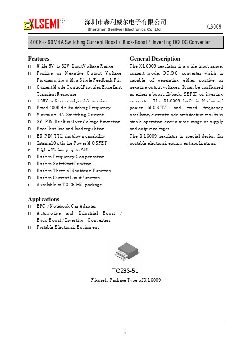
400KHz 60V 4A Switching Current Boost / Buck-Boost / Inverting DC/DC ConverterFeaturesn Wide 5V to 32V Input Voltage Rangen Positive or Negative Output Voltage Programming with a Single Feedback Pin n Current Mode Control Provides Excellent Transient Responsen 1.25V reference adjustable versionn Fixed 400KHz Switching Frequencyn Maximum 4A Switching Currentn SW PIN Built in Over Voltage Protection n Excellent line and load regulationn EN PIN TTL shutdown capabilityn Internal Optimize Power MOSFETn High efficiency up to 94%n Built in Frequency Compensationn Built in Soft-Start Functionn Built in Thermal Shutdown Functionn Built in Current Limit Functionn Available in TO263-5L package Applicationsn EPC / Notebook Car Adaptern Automotive and Industrial Boost / Buck-Boost / Inverting Convertersn Portable Electronic Equipment General DescriptionThe XL6009 regulator is a wide input range, current mode, DC/DC converter which is capable of generating either positive or negative output voltages. It can be configured as either a boost, flyback, SEPIC or inverting converter. The XL6009 built in N-channel power MOSFET and fixed frequency oscillator, current-mode architecture results in stable operation over a wide range of supply and output voltages.The XL6009 regulator is special design for portable electronic equipment applications.Figure1. Package Type of XL6009400KHz 60V 4A Switching Current Boost / Buck-Boost / Inverting DC/DC Converter Pin ConfigurationsFigure2. Pin Configuration of XL6009 (Top View)Table 1 Pin DescriptionPin Number Pin Name Description1 GND Ground Pin.2 EN Enable Pin. Drive EN pin low to turn off the device, drive it high to turn it on. Floating is default high.3 SW Power Switch Output Pin (SW).4 VIN Supply V oltage Input Pin. XL6009 operates from a 5V to 32V DC voltage. Bypass Vin to GND with a suitably large capacitor to eliminate noise on the input.5 FB Feedback Pin (FB). Through an external resistor divider network, FB senses the output voltage and regulates it. The feedback threshold voltage is 1.25V.XL6009 400KHz 60V 4A Switching Current Boost / Buck-Boost / Inverting DC/DC ConverterFunction BlockFigure3. Function Block Diagram of XL6009Typical Application CircuitFigure4. XL6009 Typical Application Circuit (Boost Converter)Shenzhen Senliwell Electronics Co.,Ltd深圳市森利威尔电子有限公司400KHz 60V 4A Switching Current Boost / Buck-Boost / Inverting DC/DC ConverterOrdering InformationPart Number Marking ID Lead Free Lead Free Packing Type XL6009E1 XL6009E1 Tube PackageTemperature RangeXL6009TRE1XL6009E1Tape & ReelXLSEMI Pb-free products, as designated with “E1” suffix in the par number, are RoHS compliant.Absolute Maximum Ratings (Note1)ParameterSymbol Value Unit Input VoltageVin -0.3 to 36 V Feedback Pin Voltage V FB -0.3 to Vin V EN Pin VoltageV EN -0.3 to Vin V Output Switch Pin Voltage V Output -0.3 to 60 V Power DissipationP D Internally limitedmW Thermal Resistance (TO263-5L)(Junction to Ambient, No Heatsink, Free Air) R JA 30 ºC/W Operating Junction Temperature T J -40 to 125 ºC Storage TemperatureT STG -65 to 150 ºC Lead Temperature (Soldering, 10 sec) T LEAD 260 ºC ESD (HBM)>2000VNote1: Stresses greater than those listed under Maximum Ratings may cause permanent damage to the device. This is a stress rating only and functional operation of the device at these or any other conditions above those indicated in the operation is not implied. Exposure to absolute maximum rating conditions for extended periods may affect reliability.400KHz 60V 4A Switching Current Boost / Buck-Boost / Inverting DC/DC ConverterXL6009 Electrical CharacteristicsT a = 25℃;unless otherwise specified.Symbol Parameter Test Condition Min. Typ. Max. Unit System parameters test circuit figure4VFB FeedbackV oltageVin = 12V to 16V, V out=18VIload=0.1A to 2A1.213 1.25 1.287 VEfficiency ŋVin=12V ,V out=18.5VIout=2A- 92 - %Electrical Characteristics (DC Parameters)Vin = 12V, GND=0V, Vin & GND parallel connect a 220uf/50V capacitor; Iout=0.5A, T a = 25℃; the others floating unless otherwise specified.Parameters Symbol Test Condition Min. Typ. Max. Unit Input operation voltage Vin 5 32 V Shutdown Supply Current I STBY V EN=0V 70 100 uAQuiescent Supply Current I q V EN =2V,V FB =Vin2.5 5 mAOscillator Frequency Fosc 320 400 480 Khz Switch Current Limit I L V FB =0 4 AOutput Power NMOS Rdson Vin=12V,I SW=4A110 120 mohmEN Pin Threshold V EN High (Regulator ON)Low (Regulator OFF)1.40.8VI H V EN =2V (ON) 3 10 uA EN Pin Input LeakageCurrent ILV EN =0V (OFF) 3 10 uA Max. Duty Cycle D MAX V FB=0V 90 %400KHz 60V 4A Switching Current Boost / Buck-Boost / Inverting DC/DC Converter Schottky Diode Selection TableCurrent SurfaceMount ThroughHoleVR (The same as system maximum input voltage)20V 30V 40V 50V60V1A √1N5817 1N5818 1N5819√1N5820 1N5821 1N5822√MBR320 MBR330 MBR340 MBR350MBR360 √SK32 SK33 SK34 SK35 SK36√30WQ03 30WQ04 30WQ05√31DQ03 31DQ04 31DQ053A√SR302 SR303 SR304 SR305 SR306√1N5823 1N5824 1N5825√SR502 SR503 SR504 SR505 SR506√SB520 SB530 SB540 SB550 SB5605A√50WQ03 50WQ04 50WQ05Typical System Application for EPC/Notebook Car Adapter – Boost (Output 18.5V/2.5A) Figure5. XL6009 Typical System Application (Boost Converter)400KHz 60V 4A Switching Current Boost / Buck-Boost / Inverting DC/DC ConverterTypical System Application for Portable Notebook Car Adapter– SEPIC Buck-Boost Topology (Input 10V~30V, Output 12V/2A)Figure6. XL6009 Typical System Application (SEPIC Buck-Boost Converter) Typical System Application for Inverting Converter– SEPIC Inverting Topology (Input 10V~30V, Output + -12V/1A)Figure7. XL6009 Typical System Application (SEPIC Inverting Converter)400KHz 60V 4A Switching Current Boost / Buck-Boost / Inverting DC/DC ConverterPackage InformationTO263-5L。
品牌授权协议书5篇篇1品牌授权协议书甲方:(授权方)地址:法定代表人:联系电话:乙方:(被授权方)地址:法定代表人:联系电话:鉴于甲方为(品牌名称)的拥有者,拥有该品牌的商标权、知识产权等相关权益;乙方希望取得甲方的授权,使用该品牌进行相关商业活动,经双方友好协商,达成如下协议:第一条授权范围1.1 甲方同意授权乙方在(授权区域范围)内合法使用甲方所有注册商标的使用权。
1.2 授权使用范围具体为:(授权范围具体描述)。
第二条版权使用期限2.1 本授权协议从双方签署之日起生效,持续(授权期限)。
2.2 授权期满后,若双方无异议,可协商续签或终止。
第三条授权费用3.1 乙方在授权期间须向甲方支付授权费用,具体数额为(授权费用)。
3.2 授权费用支付方式为(支付方式),支付时间为(支付时间)。
第四条授权义务4.1 乙方必须按照授权范围及期限使用商标,并保证商标的合法使用。
4.2 乙方不得擅自转让、出租或以其他方式交由第三方使用商标权益。
4.3 乙方在商标使用过程中,须维护商标的形象和声誉,不得进行损害商标利益的行为。
第五条保密条款5.1 双方在协商和履行本协议过程中所获得的对方的商业秘密、技术资料等信息,必须保密,不得向第三方透露。
5.2 若双方需要披露对方商业秘密时,需事先获得对方书面同意。
第六条违约责任6.1 若一方违反本协议各项条款,应承担对方的违约责任,并支付违约金(违约金数额)。
6.2 一方违约致使另一方遭受损失的,应承担相应的赔偿责任。
第七条协议解释7.1 本协议如有争议,双方应友好协商解决;若协商不成,应提交(仲裁机构)仲裁解决。
7.2 本协议经双方签字盖章确认后生效,有效期内不可擅自修改或解除。
甲方(盖章):日期:乙方(盖章):日期:以上是品牌授权协议书的具体内容,双方需遵守并执行协议约定,共同维护品牌利益,实现合作共赢。
希望双方能够真诚合作,共同推动品牌事业的发展。
篇2品牌授权协议书甲方:(公司名称、地址、法定代表人)乙方:(公司名称、地址、法定代表人)为了明确双方的权利和义务,根据《中华人民共和国合同法》和相关法律法规的规定,甲、乙双方经友好协商,就甲方授权乙方使用其品牌的事宜,达成如下协议:一、授权内容1.1 甲方授权乙方在(地区/渠道/范围)内,使用甲方自有品牌(名称、图形标识等)进行销售推广等活动。
品牌授权协议书5篇第1篇示例:关于品牌授权协议书一、授权范围鉴于甲方为【品牌名称】的合法拥有者,拥有对该品牌进行授权的权利,现甲方同意将该品牌授权给乙方使用,作为乙方的独有品牌。
该授权范围仅限于经乙方允许的使用范围内,不得擅自进行他用。
二、授权期限1. 本协议自双方签署之日起生效,至约定的授权期限届满止。
2. 授权期限届满前,若双方同意继续合作,则应在期限届满前提前30天书面通知对方,双方签署新的授权协议,方可继续合作。
三、权利义务1. 甲方权利甲方有权对使用该品牌的乙方进行监督和管理,确保乙方的使用行为符合合作协议的规定。
甲方享有对该品牌的商标权、著作权等相关权利。
2. 乙方权利乙方有权在经甲方授权下使用该品牌,作为自己的独有品牌。
乙方有义务保护该品牌的声誉和形象,不得进行损害该品牌形象的行为。
四、授权费用1. 乙方在获得使用该品牌的授权后,应按约定向甲方支付相应的授权费用。
授权费用的支付方式和时间应在双方签署的授权协议中规定。
2. 若乙方未按时支付授权费用或违反约定使用该品牌,甲方有权解除授权协议,并要求乙方赔偿相应的损失。
五、保密条款双方应对相关的商业信息和技术资料进行保密,不得将相关信息透露给第三方或用于其他用途,除非经对方书面同意。
六、争议解决双方如在履行本协议过程中出现争议,应友好协商解决。
若不能协商解决,应提交至甲方所在地人民法院进行裁决。
七、其他事项1. 本协议经双方签署后生效,具有法律效力。
2. 甲、乙双方应诚实履行本协议约定的各项义务,共同维护双方的合法权益。
3. 本协议一式两份,双方各持一份,具有同等效力。
甲方(盖章):___________乙方(盖章):___________日期:___________第2篇示例:品牌授权协议书一、授权方与受权方甲方(授权方):乙方(受权方):二、授权事项1. 甲方是【品牌名称】的合法所有者,享有该品牌的全部商标权、专利权、著作权和其他相关权利。
XL6009400KHz 60V 4A Switching Current Boost / Buck-Boost / Inverting DC/DC ConverterFeaturesn Wide 5V to 32V Input Voltage Range n Positive or Negative Output VoltageProgramming with a Single Feedback Pin n Current Mode Control Provides ExcellentTransient Responsen 1.25V reference adjustable version n Fixed 400KHz Switching Frequency n Maximum 4A Switching Currentn SW PIN Built in Over Voltage Protection n Excellent line and load regulation n EN PIN TTL shutdown capability n Internal Optimize Power MOSFET nHigh efficiency up to 94%n Built in Frequency Compensation n Built in Soft-Start Functionn Built in Thermal Shutdown Function n Built in Current Limit Function n Available in TO263-5L packageApplicationsn EPC / Notebook Car Adaptern Automotive and Industrial Boost /Buck-Boost / Inverting Converters n Portable Electronic EquipmentGeneral DescriptionThe XL6009 regulator is a wide input range, current mode, DC/DC converter which is capable of generating either positive or negative output voltages. It can be configured as either a boost, flyback, SEPIC or inverting converter. The XL6009 built in N-channel power MOSFET and fixed frequency oscillator, current-mode architecture results in stable operation over a wide range of supply and output voltages.The XL6009 regulator is special design for portable electronic equipment applications.Figure1. Package Type of XL6009技术索样QQ:1378271156400KHz 60V 4A Switching Current Boost / Buck-Boost / Inverting DC/DC Converter Pin ConfigurationsFigure2. Pin Configuration of XL6009 (Top View)Table 1 Pin DescriptionPin Number Pin Name Description1 GND Ground Pin.2 EN Enable Pin. Drive EN pin low to turn off the device, drive it high to turn it on. Floating is default high.3 SW Power Switch Output Pin (SW).4 VIN Supply V oltage Input Pin. XL6009 operates from a 5V to 32V DC voltage. Bypass Vin to GND with a suitably large capacitor to eliminate noise on the input.5 FB Feedback Pin (FB). Through an external resistor divider network, FB senses the output voltage and regulates it. The feedback threshold voltage is 1.25V.400KHz 60V 4A Switching Current Boost / Buck-Boost / Inverting DC/DC Converter Function BlockFigure3. Function Block Diagram of XL6009Typical Application CircuitFigure4. XL6009 Typical Application Circuit (Boost Converter)400KHz 60V 4A Switching Current Boost / Buck-Boost / Inverting DC/DC ConverterOrdering InformationPart Number Marking ID Lead Free Lead Free Packing Type XL6009E1 XL6009E1 Tube PackageTemperature RangeXL6009TRE1XL6009E1Tape & ReelXLSEMI Pb-free products, as designated with “E1” suffix in the par number, are RoHS compliant.Absolute Maximum Ratings (Note1)ParameterSymbol Value Unit Input VoltageVin -0.3 to 36 V Feedback Pin Voltage V FB -0.3 to Vin V EN Pin VoltageV EN -0.3 to Vin V Output Switch Pin Voltage V Output -0.3 to 60 V Power DissipationP D Internally limitedmW Thermal Resistance (TO263-5L)(Junction to Ambient, No Heatsink, Free Air) R JA 30 ºC/W Operating Junction Temperature T J -40 to 125 ºC Storage TemperatureT STG -65 to 150 ºC Lead Temperature (Soldering, 10 sec) T LEAD 260 ºC ESD (HBM)>2000VNote1: Stresses greater than those listed under Maximum Ratings may cause permanent damage to the device. This is a stress rating only and functional operation of the device at these or any other conditions above those indicated in the operation is not implied. Exposure to absolute maximum rating conditions for extended periods may affect reliability.400KHz 60V 4A Switching Current Boost / Buck-Boost / Inverting DC/DC ConverterXL6009 Electrical CharacteristicsT a = 25℃;unless otherwise specified.Symbol Parameter Test Condition Min. Typ. Max. Unit System parameters test circuit figure4VFB FeedbackV oltageVin = 12V to 16V, V out=18VIload=0.1A to 2A1.213 1.25 1.287 VEfficiency ŋVin=12V ,V out=18.5VIout=2A- 92 - %Electrical Characteristics (DC Parameters)Vin = 12V, GND=0V, Vin & GND parallel connect a 220uf/50V capacitor; Iout=0.5A, T a = 25℃; the others floating unless otherwise specified.Parameters Symbol Test Condition Min. Typ. Max. Unit Input operation voltage Vin 5 32 V Shutdown Supply Current I STBY V EN=0V 70 100 uAQuiescent Supply Current I q V EN =2V,V FB =Vin2.5 5 mAOscillator Frequency Fosc 320 400 480 Khz Switch Current Limit I L V FB =0 4 AOutput Power NMOS Rdson Vin=12V,I SW=4A110 120 mohmEN Pin Threshold V EN High (Regulator ON)Low (Regulator OFF)1.40.8VI H V EN =2V (ON) 3 10 uA EN Pin Input LeakageCurrent ILV EN =0V (OFF) 3 10 uA Max. Duty Cycle D MAX V FB=0V 90 %400KHz 60V 4A Switching Current Boost / Buck-Boost / Inverting DC/DC Converter Schottky Diode Selection TableCurrent SurfaceMount ThroughHoleVR (The same as system maximum input voltage)20V 30V 40V 50V60V1A √1N5817 1N5818 1N5819√1N5820 1N5821 1N5822√MBR320 MBR330 MBR340 MBR350MBR360 √SK32 SK33 SK34 SK35 SK36√30WQ03 30WQ04 30WQ05√31DQ03 31DQ04 31DQ053A√SR302 SR303 SR304 SR305 SR306√1N5823 1N5824 1N5825√SR502 SR503 SR504 SR505 SR506√SB520 SB530 SB540 SB550 SB5605A√50WQ03 50WQ04 50WQ05Typical System Application for EPC/Notebook Car Adapter – Boost (Output 18.5V/2.5A) Figure5. XL6009 Typical System Application (Boost Converter)400KHz 60V 4A Switching Current Boost / Buck-Boost / Inverting DC/DC ConverterTypical System Application for Portable Notebook Car Adapter– SEPIC Buck-Boost Topology (Input 10V~30V, Output 12V/2A)Figure6. XL6009 Typical System Application (SEPIC Buck-Boost Converter) Typical System Application for Inverting Converter– SEPIC Inverting Topology (Input 10V~30V, Output + -12V/1A)Figure7. XL6009 Typical System Application (SEPIC Inverting Converter)400KHz 60V 4A Switching Current Boost / Buck-Boost / Inverting DC/DC ConverterPackage InformationTO263-5L。
品牌授权协议范本完整版5篇篇1甲方(授权方):_________________________乙方(被授权方):_______________________鉴于甲方拥有自主知识产权的品牌,并希望将该品牌授权给乙方使用,双方本着平等互利、合作共赢的原则,经友好协商,达成如下品牌授权协议:一、协议目的甲方授权乙方使用其拥有的品牌,允许乙方在特定范围内进行品牌宣传、销售等活动,共同提升品牌价值,实现共赢发展。
二、授权内容1. 甲方将其所拥有的品牌(以下简称“本品牌”)授权给乙方使用,授权范围包括但不限于产品销售、广告宣传、市场推广等。
2. 乙方有权在授权范围内使用本品牌的商标、标识、名称等,并有权在相关产品或包装上使用本品牌标识。
3. 乙方应按照甲方的要求,在授权范围内进行品牌宣传和推广活动,维护本品牌的声誉和形象。
三、授权期限本协议自双方签署之日起生效,有效期为_____年。
到期后,如双方继续合作,可续签本协议。
四、双方责任与义务1. 甲方应保证本品牌的合法权益,并保证授权乙方的使用权不受第三方干扰。
2. 乙方应合法使用本品牌,不得侵犯甲方的知识产权。
3. 乙方应遵守甲方的品牌管理规范,维护本品牌的声誉和形象。
4. 乙方应向甲方支付品牌使用费,具体金额和支付方式详见附件。
5. 甲乙双方应共同保护本品牌的知识产权,不得将本品牌泄露给第三方。
五、保密条款1. 双方同意在本协议执行过程中了解到的对方商业秘密及其他相关信息予以保密。
2. 未经对方许可,任何一方不得向第三方泄露本协议内容以及双方在合作过程中了解到的对方商业秘密及其他相关信息。
六、违约责任1. 若甲方违反本协议规定,导致乙方无法正常使用本品牌,乙方有权要求甲方承担违约责任,并赔偿乙方因此造成的损失。
2. 若乙方违反本协议规定,侵犯甲方的知识产权或违反品牌管理规范,甲方有权要求乙方承担违约责任,并赔偿甲方因此造成的损失。
七、争议解决因执行本协议所引起的任何争议,双方应通过友好协商解决。
400KHz 60V 4A Switching Current Boost / Buck-Boost / Inverting DC/DC ConverterFeaturesn Wide 5V to 32V Input Voltage Rangen Positive or Negative Output Voltage Programming with a Single Feedback Pin n Current Mode Control Provides Excellent Transient Responsen 1.25V reference adjustable versionn Fixed 400KHz Switching Frequencyn Maximum 4A Switching Currentn SW PIN Built in Over Voltage Protection n Excellent line and load regulationn EN PIN TTL shutdown capabilityn Internal Optimize Power MOSFETn High efficiency up to 94%n Built in Frequency Compensationn Built in Soft-Start Functionn Built in Thermal Shutdown Functionn Built in Current Limit Functionn Available in TO263-5L package Applicationsn EPC / Notebook Car Adaptern Automotive and Industrial Boost / Buck-Boost / Inverting Convertersn Portable Electronic Equipment General DescriptionThe XL6009 regulator is a wide input range, current mode, DC/DC converter which is capable of generating either positive or negative output voltages. It can be configured as either a boost, flyback, SEPIC or inverting converter. The XL6009 built in N-channel power MOSFET and fixed frequency oscillator, current-mode architecture results in stable operation over a wide range of supply and output voltages.The XL6009 regulator is special design for portable electronic equipment applications.Figure1. Package Type of XL6009400KHz 60V 4A Switching Current Boost / Buck-Boost / Inverting DC/DC Converter Pin ConfigurationsFigure2. Pin Configuration of XL6009 (Top View)Table 1 Pin DescriptionPin Number Pin Name Description1 GND Ground Pin.2 EN Enable Pin. Drive EN pin low to turn off the device, drive it high to turn it on. Floating is default high.3 SW Power Switch Output Pin (SW).4 VIN Supply V oltage Input Pin. XL6009 operates from a 5V to 32V DC voltage. Bypass Vin to GND with a suitably large capacitor to eliminate noise on the input.5 FB Feedback Pin (FB). Through an external resistor divider network, FB senses the output voltage and regulates it. The feedback threshold voltage is 1.25V.400KHz 60V 4A Switching Current Boost / Buck-Boost / Inverting DC/DC Converter Function BlockFigure3. Function Block Diagram of XL6009Typical Application CircuitFigure4. XL6009 Typical Application Circuit (Boost Converter)400KHz 60V 4A Switching Current Boost / Buck-Boost / Inverting DC/DC ConverterOrdering InformationPart Number Marking ID Lead Free Lead Free Packing Type XL6009E1 XL6009E1 Tube PackageTemperature RangeXL6009TRE1XL6009E1Tape & ReelXLSEMI Pb-free products, as designated with “E1” suffix in the par number, are RoHS compliant.Absolute Maximum Ratings (Note1)ParameterSymbol Value Unit Input VoltageVin -0.3 to 36 V Feedback Pin Voltage V FB -0.3 to Vin V EN Pin VoltageV EN -0.3 to Vin V Output Switch Pin Voltage V Output -0.3 to 60 V Power DissipationP D Internally limitedmW Thermal Resistance (TO263-5L)(Junction to Ambient, No Heatsink, Free Air) R JA 30 ºC/W Operating Junction Temperature T J -40 to 125 ºC Storage TemperatureT STG -65 to 150 ºC Lead Temperature (Soldering, 10 sec) T LEAD 260 ºC ESD (HBM)>2000VNote1: Stresses greater than those listed under Maximum Ratings may cause permanent damage to the device. This is a stress rating only and functional operation of the device at these or any other conditions above those indicated in the operation is not implied. Exposure to absolute maximum rating conditions for extended periods may affect reliability.400KHz 60V 4A Switching Current Boost / Buck-Boost / Inverting DC/DC ConverterXL6009 Electrical CharacteristicsT a = 25℃;unless otherwise specified.Symbol Parameter Test Condition Min. Typ. Max. Unit System parameters test circuit figure4VFB FeedbackV oltageVin = 12V to 16V, V out=18VIload=0.1A to 2A1.213 1.25 1.287 VEfficiency ŋVin=12V ,V out=18.5VIout=2A- 92 - %Electrical Characteristics (DC Parameters)Vin = 12V, GND=0V, Vin & GND parallel connect a 220uf/50V capacitor; Iout=0.5A, T a = 25℃; the others floating unless otherwise specified.Parameters Symbol Test Condition Min. Typ. Max. Unit Input operation voltage Vin 5 32 V Shutdown Supply Current I STBY V EN=0V 70 100 uAQuiescent Supply Current I q V EN =2V,V FB =Vin2.5 5 mAOscillator Frequency Fosc 320 400 480 Khz Switch Current Limit I L V FB =0 4 AOutput Power NMOS Rdson Vin=12V,I SW=4A110 120 mohmEN Pin Threshold V EN High (Regulator ON)Low (Regulator OFF)1.40.8VI H V EN =2V (ON) 3 10 uA EN Pin Input LeakageCurrent ILV EN =0V (OFF) 3 10 uA Max. Duty Cycle D MAX V FB=0V 90 %400KHz 60V 4A Switching Current Boost / Buck-Boost / Inverting DC/DC Converter Schottky Diode Selection TableCurrent SurfaceMount ThroughHoleVR (The same as system maximum input voltage)20V 30V 40V 50V60V1A √1N5817 1N5818 1N5819√1N5820 1N5821 1N5822√MBR320 MBR330 MBR340 MBR350MBR360 √SK32 SK33 SK34 SK35 SK36√30WQ03 30WQ04 30WQ05√31DQ03 31DQ04 31DQ053A√SR302 SR303 SR304 SR305 SR306√1N5823 1N5824 1N5825√SR502 SR503 SR504 SR505 SR506√SB520 SB530 SB540 SB550 SB5605A√50WQ03 50WQ04 50WQ05Typical System Application for EPC/Notebook Car Adapter – Boost (Output 18.5V/2.5A) Figure5. XL6009 Typical System Application (Boost Converter)400KHz 60V 4A Switching Current Boost / Buck-Boost / Inverting DC/DC ConverterTypical System Application for Portable Notebook Car Adapter– SEPIC Buck-Boost Topology (Input 10V~30V, Output 12V/2A)Figure6. XL6009 Typical System Application (SEPIC Buck-Boost Converter) Typical System Application for Inverting Converter– SEPIC Inverting Topology (Input 10V~30V, Output + -12V/1A)Figure7. XL6009 Typical System Application (SEPIC Inverting Converter)400KHz 60V 4A Switching Current Boost / Buck-Boost / Inverting DC/DC ConverterPackage InformationTO263-5L400KHz 60V 4A Switching Current Boost / Buck-Boost / Inverting DC/DC ConverterFeaturesn Wide 5V to 32V Input Voltage Rangen Positive or Negative Output Voltage Programming with a Single Feedback Pin n Current Mode Control Provides Excellent Transient Responsen 1.25V reference adjustable versionn Fixed 400KHz Switching Frequencyn Maximum 4A Switching Currentn SW PIN Built in Over Voltage Protection n Excellent line and load regulationn EN PIN TTL shutdown capabilityn Internal Optimize Power MOSFETn High efficiency up to 94%n Built in Frequency Compensationn Built in Soft-Start Functionn Built in Thermal Shutdown Functionn Built in Current Limit Functionn Available in TO263-5L package General DescriptionThe XL6009 regulator is a wide input range, current mode, DC/DC converter which is capable of generating either positive or negative output voltages. It can be configured as either a boost, flyback, SEPIC or inverting converter. The XL6009 built in N-channel power MOSFET and fixed frequency oscillator, current-mode architecture results in stable operation over a wide range of supply and output voltages.The XL6009 regulator is special design for portable electronic equipment applications.。