开发评估板使用说明
- 格式:pdf
- 大小:830.04 KB
- 文档页数:19

User's GuideSNVA082B–March2004–Revised May2013AN-1314LM5020Evaluation Board1IntroductionThe LM5020evaluation board is designed to provide the design engineer with a fully functional non-isolated flyback power converter to evaluate the LM5020controller.The performance of the evaluation board is as follows:•Input range:30V to75V(100V peak)•Output voltage:3.3V•Output current:0.2to4.5A•Measured efficiency:85%at1.5A,83%at4.5A•Board size:1.25×2.5×0.5inches•Load Regulation:1.5%•Line Regulation:0.1%•Line UVLO,Current LimitThe printed circuit board consists of2layers of2ounce copper on FR4material with a total thickness of0.050inches.Soldermask has been omitted from some areas to facilitate cooling.The unit is designed forcontinuous operation at rated load at<40°C with normal convection cooling.2Theory of OperationThe flyback converter is an inductive based converter in which inductive energy is stored by applying a voltage across an inductor in a similar manner to that of a boost converter.Here the similarity ends.Asecond coupled winding of the inductor transfers the energy to a secondary side rectifier after the voltage has been removed from the first winding.This allows the converter input and output grounds to beconfigured either isolated or non-isolated.There is also a voltage/current ratio change possible by altering the winding ratio between the first winding and the second winding.A semi-regulated auxiliary winding can also be provided.The flyback transformer is actually a coupled inductor with multiple windings wound on a single core.For simplification,we will refer to the first,driven winding,as the primary and the main output winding as the secondary winding of the flyback transformer.The transformer’s primary inductance is typically made as large as is practical.However,the airgapnecessary to store the cycle energy lowers the obtainable inductance.The higher the primary inductance, the less input ripple current will be generated and the less input filtering will be required.As shown,the LM5020directly drives a MOSFET switch to apply voltage across the primary.When the switch turns off,the secondary applies a forward current to the output rectifier and charges the outputcapacitor.In applications where the input voltage is considerably higher than the output voltage,the turns ratio between primary and secondary will reflect the input/output voltage ratio and the duty cycle.The LM5020is a full-featured controller providing an internal start-up regulator,soft start,over-current and under-voltage lockout.All trademarks are the property of their respective owners.1 SNVA082B–March2004–Revised May2013AN-1314LM5020Evaluation Board Submit Documentation FeedbackCopyright©2004–2013,Texas Instruments IncorporatedPowering and Loading Considerations Figure1.Simplified Flyback Converter3Powering and Loading ConsiderationsWhen applying power to the LM5020evaluation board certain precautions should be followed.TheLM5020evaluation board is quite forgiving of load and input power variations.The possibility of shipping damage or infant failure is always a concern at first power-up.4Proper ConnectionsBe sure to choose the correct wire size when attaching the source supply and the load.Monitor thecurrent into and out of the UUT.Monitor the voltages in and out directly at the terminals of the UUT.The voltage drop across the connecting wires will yield inaccurate measurements.For accurate efficiencymeasurements,these precautions are especially important.5Source PowerAt low input line voltage(30V)the input current will be approximately0.63A,while at high input linevoltage the input current will be approximately0.23.Therefore to fully test the LM5020evaluation board a DC power supply capable of at least75V and1A is required.The power supply must have adjustments for both voltage and current.An accurate readout of output current is desirable since the current is not subject to loss in the cables as voltage is.The power supply and cabling must present a low impedance to the UUT.Insufficient cabling or a high impedance power supply will cause droop during power supply application with the UUT inrush current.If large enough,this droop will cause a chattering condition upon power up.This chattering condition is an interaction with the UUT undervoltage lockout,the cabling impedance and the inrush current.6LoadingAn appropriate electronic load specified for operation down to2.0V is desirable.The maximum loadcurrent is specified as4.5A.Minimum load is specified at5%or0.23A.The resistance of a maximum load is0.73Ω(including cables).The resistance of a minimum load is14.4Ω.2AN-1314LM5020Evaluation Board SNVA082B–March2004–Revised May2013Submit Documentation FeedbackCopyright©2004–2013,Texas Instruments Incorporated Powering Up7Powering UpUsing the shutdown feature provided on the UUT will allow powering up the source supply initially with a low current level.It is suggested that the load be kept reasonably low during the first power up.Set the current limit of the source supply to provide about 1½times the wattage of the load.As you remove the connection from the shutdown pin to ground,immediately check for 3.3volts at the output.If more than a couple of seconds pass without seeing an output voltage,remove input power.A quick efficiency check is the best way to confirm that the UUT is operating properly.If something is amiss you can be reasonably sure that it will affect the efficiency adversely.Few parameters can beincorrect in a switching power supply without creating additional losses and potentially damaging heat.An efficiency above 80%is expected.After the unit is verified operationally,it can be powered up without use of the shutdown pin.8Typical Evaluation SetupFigure 2.Typical Evaluation Setup9Performance Characteristics 9.1Turn-on WaveformsWhen applying power to the LM5020evaluation board a certain sequence of events must occur.The soft-start feature allows for a minimal output voltage for a short time until the feedback loop can stabilize without overshoot.Figure 3,Figure 4,and Figure 5show typical turn-on waveforms at no load,5%load,and at full load.Input voltage,output voltage and output current are shown.Figure 6shows the initial ramp-up of the Vcc pin to 7.7volts through the internal regulator.The auxiliary winding starts to supply a higher voltage as the output voltage rises.The resulting second ramp is shown following the soft-start delay.This sequence is nearly identical for all loads and input voltages.Trace 1:Input Voltage,at 30VDC.Volts/div =20.0V Trace 2:Trace 1:Input Voltage,at 30VDC.Volts/div =20.0V Trace 2:Output Voltage,no load.Volts/div =2.0V Trace 3:Output Output Voltage,at 5%load.Volts/div =2.0V Trace 3:Output Current,no load.Amps/div =100mA Horizontal Resolution =Current,at 5%load.Amps/div =100mA Horizontal 1.0ms/div Resolution =1.0ms/divFigure 3.Typical Turn-on Waveforms at No LoadFigure 4.Typical Turn-on Waveforms at 5%Load3SNVA082B–March 2004–Revised May 2013AN-1314LM5020Evaluation BoardSubmit Documentation FeedbackCopyright ©2004–2013,Texas Instruments IncorporatedPerformance Characteristics Trace 1:Input Voltage,at 30VDC.Volts/div =20.0V Trace 2:Trace 1:VCC pin with VIN =30VDC,Load =4.5A Volts/div Output Voltage,at full load.Volts/div =2.0V Trace 3:Output =5.0V Trace 2:VIN approaching 30VDC Volts/div =20.0V Current,at full load.Amps/div =2.0A Horizontal Resolution Horizontal Resolution =2.0ms/div=1.0ms/divFigure 5.Typical Turn-on Waveforms at Full LoadFigure 6.Initial Ramp-up of the Vcc Pin to 7.7VThrough the Internal Regulator9.2Load Step ResponseFigure 7shows the load step response at Vin =30VDC for an instantaneous load change from 5%to full load.The input voltage,output voltage and output current are shown.9.3Ripple Voltage and Ripple CurrentFigure 8shows the output ripple voltage,the output ripple current and the input ripple current relative to the LM5020gate drive.Trace 1:Input Voltage,at 30VDC Volts/div =20.0V Trace 2:Trace 1:Q1gate drive at Vin =48VDC Volts/div =20.0V Output Voltage,at 3.3VDC Volts/div =2.0V Trace 3:Load Trace 2:Output ripple voltage Volts/div =100mV Trace 3:changing from 0.23A to 4.5A instantaneously Amps/div =Output ripple current Amps/div =20.0mA Trace 4:Input 2.0A Horizontal Resolution =1.0ms/divripple current Amps/div =100mA Horizontal Resolution =2.0µs/divFigure 7.Load Step Response at Vin =30VDC for an Figure 8.Output Ripple Voltage,Output RippleInstantaneous Load Change from 5%to Full Load Current,and Input Ripple Current4AN-1314LM5020Evaluation BoardSNVA082B–March 2004–Revised May 2013Submit Documentation FeedbackCopyright ©2004–2013,Texas Instruments Incorporated Performance Characteristics 9.4Transformer WaveformsFigure9,Figure10,and Figure11show typical waveforms at the junction of Q1MOSFET and thetransformer primary winding.Also shown are typical waveforms at the junction of the transformersecondary and the output rectifier,D3.Figure9reflects an input voltage of30VDC and a load of4.5A.Figure10reflects an input voltage of50VDC with the same load.Figure11reflects an input voltage of 75VDC,also at full load.Trace1:Drain of Q1at Vin=30VDC;Volts/div=50.0VTrace2:Anode of D3;Volts/div=10.0VHorizontal Resolution=0.5µs/divFigure9.Typical WaveformsTrace1:Drain of Q1at Vin=50VDC;Volts/div=50.0VTrace2:Anode of D3;Volts/div=10.0VHorizontal Resolution=0.5µs/divFigure10.Typical WaveformsTrace1:Drain of Q1at Vin=75VDC;Volts/div=50.0VTrace2:Anode of D3;Volts/div=10.0VHorizontal Resolution=0.5µs/divFigure11.Typical Waveforms5 SNVA082B–March2004–Revised May2013AN-1314LM5020Evaluation Board Submit Documentation FeedbackCopyright©2004–2013,Texas Instruments IncorporatedBill of Materials 10Bill of MaterialsThe Bill of Materials is listed in Table1and includes the manufacturer and part number.Table1.Bill of MaterialsDesignator Description Manufacturer Part Number C1 2.2µF,100V,CER,X7R,1812TDK C4532X7R2A225MC2 2.2µF,100V,CER,X7R,1812TDK C4532X7R2A225MC30.01µF,50V,CER,X7R,0805TDK C2012X7R1H103KC40.1µF,100V,CER,X7R,1206TDK C3216X7R2A104KC50.01µF,50V,CER,X7R,0805TDK C2012X7R1H103KC6220pF,50V,CER,COG,0805TDK C2012COG1H221JC73300pF,50V,CER,COG,0805TDK C2012COG1H332KC8100pF,50V,CER,COG,0805TDK C2012COG1H101JC90.1µF,50V,CER,X7R,0805TDK C2012X7R1H104KC10 4.7µF,16V,CER,X7R,1206TDK C3216X7R1C475KC111000pF,50V,CER,COG,0805TDK C2012COG1H102JC12470pF,50V,CER,COG,0805TDK C2012COG1H471JC13100µF,4V,CER,X7S,1812TDK C4532X7S0G107MC14100µF,4V,CER,X7S,1812TDK C4532X7S0G107MC15270µF,4V,ALUM ORG,3018PKG KEMET A700X277M0004ATD1DUAL,SIGNAL,COM CATH,SOT-23CENTRAL SEMICONDUCTOR CMPD2838E-NSAD2DUAL,SIGNAL,COM CATH,SOT-23CENTRAL SEMICONDUCTOR CMPD2838E-NSAD3SCHOTTKY RECT,8A,35V,D2PAK ON SEMICONDUCTOR MBRD835LJ1TERMINAL BLOCK,SCREW,2POS PHOENIX CONTACT MKDS½-3.81J2TERMINAL BLOCK,SCREW,2POS PHOENIX CONTACT MKDS½-3.81Q1MOSFET,N-CH,150V,85mΩ,PWR SO8VISHAY/SILICONIX Si7898DPR110.0Ω,1%,THICK FILM,1206VISHAY CRCW120610R0JR261.9K,1%,THICK FILM,1206VISHAY CRCW12066192FR3 2.87K,1%,THICK FILM,0805VISHAY CRCW08052871FR4 1.00K,1%,THICK FILM,0805VISHAY CRCW08051001FR515.0K,1%,THICK FILM,0805VISHAY CRCW08051502FR612.4K,1%,THICK FILM,0805VISHAY CRCW08051242FR7100Ω,1%,THICK FILM,0805VISHAY CRCW08051000FR80.47Ω,1%,THICK FILM,1206VISHAY CRCW12060R47FR90.47Ω,1%,THICK FILM,1206VISHAY CRCW12060R47FR1010.0Ω,1%,1W,THICK FILM,2512VISHAY CRCW251210R0JR11 2.43K,1%,THICK FILM,0805VISHAY CRCW08052431FR12 1.47K,1%,THICK FILM,0805VISHAY CRCW08051471FR1320.0Ω,1%,THICK FILM,0805VISHAY CRCW080520R0FSD TERMINAL,SMALL TEST POINT KEYSTONE5002SYNC TERMINAL,SMALL TEST POINT KEYSTONE5002T1TRANSFORMER,FLYBACK,EFD20COILCRAFT B0695-AOR T1TRANSFORMER,FLYBACK,EFD20PULSE PA0751U1CONTROLLER,SINGLE OUT,PWM,VSSOP-10TEXAS INSTRUMENTS LM5020Z1ZENER,30V,SMB PKG.ON SEMICONDUCTOR1SMB5936B6AN-1314LM5020Evaluation Board SNVA082B–March2004–Revised May2013Submit Documentation FeedbackCopyright©2004–2013,Texas Instruments Incorporated PCB Layouts 11PCB LayoutsThe layers of the printed circuit board are shown in top down order.View is from the top down.Scale is approximately X2.0.The printed circuit board consists of2layers of2ounce copper on FR4material witha total thickness of0.050inches.7 SNVA082B–March2004–Revised May2013AN-1314LM5020Evaluation Board Submit Documentation FeedbackCopyright©2004–2013,Texas Instruments IncorporatedPCB Layouts 8AN-1314LM5020Evaluation Board SNVA082B–March2004–Revised May2013Submit Documentation FeedbackCopyright©2004–2013,Texas Instruments Incorporated PCB Layouts9 SNVA082B–March2004–Revised May2013AN-1314LM5020Evaluation Board Submit Documentation FeedbackCopyright©2004–2013,Texas Instruments IncorporatedIMPORTANT NOTICETexas Instruments Incorporated and its subsidiaries(TI)reserve the right to make corrections,enhancements,improvements and other changes to its semiconductor products and services per JESD46,latest issue,and to discontinue any product or service per JESD48,latest issue.Buyers should obtain the latest relevant information before placing orders and should verify that such information is current and complete.All semiconductor products(also referred to herein as“components”)are sold subject to TI’s terms and conditions of sale supplied at the time of order acknowledgment.TI warrants performance of its components to the specifications applicable at the time of sale,in accordance with the warranty in TI’s terms and conditions of sale of semiconductor products.Testing and other quality control techniques are used to the extent TI deems necessary to support this warranty.Except where mandated by applicable law,testing of all parameters of each component is not necessarily performed.TI assumes no liability for applications assistance or the design of Buyers’products.Buyers are responsible for their products and applications using TI components.To minimize the risks associated with Buyers’products and applications,Buyers should provide adequate design and operating safeguards.TI does not warrant or represent that any license,either express or implied,is granted under any patent right,copyright,mask work right,or other intellectual property right relating to any combination,machine,or process in which TI components or services are rmation published by TI regarding third-party products or services does not constitute a license to use such products or services or a warranty or endorsement e of such information may require a license from a third party under the patents or other intellectual property of the third party,or a license from TI under the patents or other intellectual property of TI.Reproduction of significant portions of TI information in TI data books or data sheets is permissible only if reproduction is without alteration and is accompanied by all associated warranties,conditions,limitations,and notices.TI is not responsible or liable for such altered rmation of third parties may be subject to additional restrictions.Resale of TI components or services with statements different from or beyond the parameters stated by TI for that component or service voids all express and any implied warranties for the associated TI component or service and is an unfair and deceptive business practice. TI is not responsible or liable for any such statements.Buyer acknowledges and agrees that it is solely responsible for compliance with all legal,regulatory and safety-related requirements concerning its products,and any use of TI components in its applications,notwithstanding any applications-related information or support that may be provided by TI.Buyer represents and agrees that it has all the necessary expertise to create and implement safeguards which anticipate dangerous consequences of failures,monitor failures and their consequences,lessen the likelihood of failures that might cause harm and take appropriate remedial actions.Buyer will fully indemnify TI and its representatives against any damages arising out of the use of any TI components in safety-critical applications.In some cases,TI components may be promoted specifically to facilitate safety-related applications.With such components,TI’s goal is to help enable customers to design and create their own end-product solutions that meet applicable functional safety standards and requirements.Nonetheless,such components are subject to these terms.No TI components are authorized for use in FDA Class III(or similar life-critical medical equipment)unless authorized officers of the parties have executed a special agreement specifically governing such use.Only those TI components which TI has specifically designated as military grade or“enhanced plastic”are designed and intended for use in military/aerospace applications or environments.Buyer acknowledges and agrees that any military or aerospace use of TI components which have not been so designated is solely at the Buyer's risk,and that Buyer is solely responsible for compliance with all legal and regulatory requirements in connection with such use.TI has specifically designated certain components as meeting ISO/TS16949requirements,mainly for automotive use.In any case of use of non-designated products,TI will not be responsible for any failure to meet ISO/TS16949.Products ApplicationsAudio /audio Automotive and Transportation /automotiveAmplifiers Communications and Telecom /communicationsData Converters Computers and Peripherals /computersDLP®Products Consumer Electronics /consumer-appsDSP Energy and Lighting /energyClocks and Timers /clocks Industrial /industrialInterface Medical /medicalLogic Security /securityPower Mgmt Space,Avionics and Defense /space-avionics-defense Microcontrollers Video and Imaging /videoRFID OMAP Applications Processors /omap TI E2E Community Wireless Connectivity /wirelessconnectivityMailing Address:Texas Instruments,Post Office Box655303,Dallas,Texas75265Copyright©2013,Texas Instruments Incorporated。
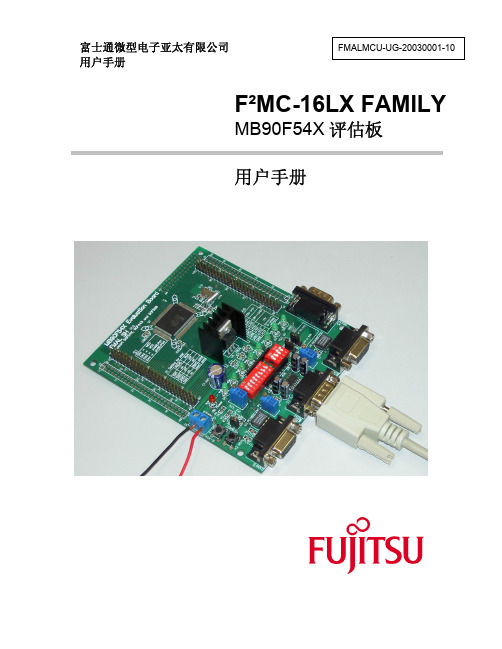
富士通微型电子亚太有限公司FMALMCU-UG-20030001-10用户手册F²MC-16LX FAMILYMB90F54X评估板用户手册版本历史日期 版本 更改内容/备注 更改人2003年5月15日 1.0 1.0 版完成 David目 录版本历史目录1 总论 (1)1.1 概况 (1)1.2 简介 (1)2 板上功能 (2)3 评估板支持的单片机 (2)4 评估板的配置 (2)4.1 基本配置 (2)4.2 CAN控制器配置 (2)4.3 A/D功能的使用配置 (3)5 用Accemic MDE调试评估板 (3)6 接口 (4)6.1电源接口(X1) (4)6.2 引脚排针(J1, J2, J3, J4) (4)6.3 UART通用异步口 (X2, X3) (4)6.4 CAN 接口 (X4, X5) (4)7 物品清单 (5)8 相关网址及联系方式 (6)附录:A. PCB丝印图 (7)B. 电路原理图............................................................ (8)1 总论1.1 概况本手册概括介绍了MB90F54X 评估板。
本板可以用来评估富士通的16LX系列单片机中的MB90F540、MB90F545系列, MB90F443和MB90F598。
1.2 简介MB90F54X 评估板是为了支持开发人员进行低成本和快速开发而设计的。
其特性如下:• 支持Accemic MDE调试环境。
Accemic MDE这是一个低成本的并简单易用的硬件调试环境,由富士通的第三方公司Accemic开发,支持富士通的大多数16位和部分32位单片机。
• 内部集成的CAN控制器。
CAN是一个串行、异步、多主通讯协议,在汽车和工业控制中被广泛应用于电子控制单元之间的通讯。
• 支持Flash的在线烧写。
不需烧写器,可方便进行软件在线升级。
• 支持Flash加密。

General DescriptionThe MAX1464 evaluation kit (EV kit) is designed to evaluate the MAX1464 high-performance, low-power, low-noise multichannel sensor signal processor. The EV kit includes: an evaluation PCB, the EV board that contains a MAX1464 signal conditioner with a typical application circuit, and potentiometers that act as sensor inputs to the MAX1464; an interface PCB, KEY, which acts as a voltage level translator between the EV kit and the com-puter; a parallel-port extension cable; plus, supporting software, program examples,and related documenta-tion and application notes.The DB25 pin connector allows a PC’s parallel port to provide the interface. Two Windows ®-based software (hardware debugger and control program) provide a friendly graphics user interface (GUI) to utilize the fea-tures of the MAX1464, as well as to perform sensor compensation of one device. The Hardware Debugger program includes multiple tabs for accessing relevant registers and ports, writing programs to the on-chip flash memory, downloading flash memory contents into a file,etc. Use the Hardware Debugger program to learn the MAX1464 functions and see the significance of individ-ual registers and ports. The Control program includes functional buttons to have the chip perform a series of predefined lower level operations, such as pushing sin-gle buttons to read the ADC. The Control program can be used to perform 2nd-order sensor compensation and calibration.The EV board can be powered by either a fixed +5V supply or by an +8V to +40V supply that is regulated to +5V by a regulator present on the EV kit board before it is applied to the MAX1464 chip. J umper J U1 must be set consistently with the used power supply.Order the MAX1464 EV kit for comprehensive evaluation of the MAX1464 using a PC with an available parallel port.Windows is a registered trademark of Microsoft Corp.Features♦Proven PCB Layout♦Windows 98/NT/2000/XP Compatible♦On-Board Potentiometers Act as Sensor Inputs ♦Spare Area for Simple-Circuit Breadboarding ♦LEDs for Visual Verification ♦+5V or +8V to +40V Possible Supply ♦Included Interconnect Cables ♦Included Additional SamplesEvaluates: MAX1464MAX1464 Evaluation Kit________________________________________________________________Maxim Integrated Products 119-0582; Rev 0; 12/06For pricing, delivery, and ordering information,please contact Maxim/Dallas Direct!at1-888-629-4642, or visit Maxim’s website at .Ordering InformationComponent SuppliersMAX1464 EV Kit FilesComponent ListEV Kit Component Listing these component suppliers.E v a l u a t e s : M A X 1464MAX1464 Evaluation Kit 2Component List (continued)Interface Board (KEY) Component ListQuick StartRequired Equipment •MAX1464 EV kit• A fixed +5VDC power supply•Computer running Windows 98/NT/2000/XP with an available parallel port (USB-to-parallel-port convert-ers not supported)•A multimeter•One parallel (printer) cableNote:In the following sections, software-related items are identified by bolding. Text in bold refers to items directly from the EV kit software. Text in bold and underlined refers to items from the Windows 98SE/2000/XP operating system.Procedures Applying Power to the MAX1464 EV Board 1)Verify that all jumpers on the EV kit board are setper the default setting shown in Table 1.2)Connect a fixed +5V power supply to the EV kitboard TB2 +5V terminal.3)The LEDs on the EV kit board start blinking. TheMAX1464 EV kit is shipped with a program, EVTEST1.hex, preloaded in the MAX1464 flash memory. This program alternatively flashes the two LEDs on the EV board.Setting Up for Digital Communication 1)Download the latest MAX1464 software from theMaxim website.2)Start the INSTALL.EXE program and follow theinstructions to install all MAX1464 applications pro-grams and to copy supporting files to your computer.3)Set up the MAX1464 EV kit by connecting the EVboard and the KEY using the 16-pin ribbon cable.Connect the KEY to the PC’s parallel port using a 25-pin straight-through, female-to-male cable.Example of Using the Hardware Debugger 1)Start the Hardware Debugger program from Start |MAX1464 EV kit | Hardware Debugger.2) A window (Figure 1) appears on the monitor.3)Read the text in the window next to the Check CPUstatus on the top row and verify that it reads Running or Halted. Any other reading indicates a hardware and/or setup problem. Fix the problem before continuing to the next step. The next few steps detail loading a new LED double blinking pro-gram to the MAX1464 flash memory and running it.4)Press the Flash Memory tab in the HardwareDebugger window.5)Press Load Buffer from file tab.6)Select … | MAX1464 | examples | cctmr1-64.hexfile to read the .hex file and save it in the temporarybuffer.7)Press Write to device tab to write the cctmr1-64.hexprogram to the flash memory.8)Press Verify device against buffer to verify that theflash memory write operation is successful.9)Execute the LED double-blinking program bypressing on the Run CPU button. The LEDs startblinking. This process verifies that the EV kit con-nections are correct, the EV board jumpers are setcorrectly, and the computer interface is working.Example of Using the Control Program Note:Exit the Hardware Debugger before starting theControl program.This section demonstrates how to start the Controlprogram and make the basic measurement of the inputvoltage.1)Start the Control program from Start | MAX1464EV kit | Control Program.2) A window (Figure 2) appears on the monitor.3)The DUT?button turns green if the hardware setupis correct and communication with the MAX1464 isestablished. A red button indicates a hardwareand/or setup problem. The next few steps detailreading the signal applied on the MAX1464 inputand write to the Data Array, which is the input tothe compensation algorithm.4)Set the value of This Temp Point and This PressPoint to match one of the test conditions displayedin the Data Array.5)Press the Read ADC button to convert the on-chiptemperature sensor output and channel 1 input volt-age and display the results of both conversions inthe Data Array.6)To read other input voltages, adjust VR1 and VR2potentiometers and repeat steps 5 and 6.7)Refer to the MAX1464 Control program manual fora full description of Control program capabilities.Evaluates: MAX1464 MAX1464 Evaluation Kit_______________________________________________________________________________________3E v a l u a t e s : M A X 1464Detailed Software DescriptionTwo independent programs have been provided for the MAX1464 to aid the user in evaluating and designing in the MAX1464 signal conditioner into a product.Hardware DebuggerThe hardware debugger program includes multiple tabs for accessing the relevant registers and ports,writing programs to the on-chip flash memory, down-loading flash memory contents into a file, etc. Use the hardware debugger program to learn the MAX1464functions, registers, and ports.CPU Registers r0..rf, p0..pfIn this window, users can read/write the CPU (module)registers, program counter r0, r1. Users can also read/write the CPU ports p0 through pf when the CPU is halted.ADC ModuleIn this window, users can access the ADC control, ADC configuration, and ADC data registers for all three chan-nels (channel 1, channel 2, and temperature sensor).DOP ModuleIn this window, users can access the DOP control, DOP configuration, and DOP data registers for both output channels and the op amp configuration register.Other ModulesIn this window, users can access registers related to the timer, power control, oscillator, and GPIOs.Flash MemoryThis window can be used for all flash-memory opera-tions, such as writing flash memory to/from a file.Program ListingIn this window, users can view the list file of an assem-bly program. Select the filename from the File pulldown menu.MAX1464 Evaluation Kit 4_______________________________________________________________________________________Figure 1. Hardware Debugger WindowControl Program (MAX1464 Main.exe) The Control program includes functional buttons to have the MAX1464 perform a series of predefined lower level operations, such as reading the ADC, loading a file into flash memory, etc. The Control program can be used to perform a 2nd-order temperature compensation.The main purpose of the Control program is to provide the user with a tool to easily compensate a sensor. The compensation algorithm defined in Application Note 3649, MAX1464 Signal-Conditioner, Sensor Compensation Algorithm, has been implemented. All the user needs to do is to properly set up the EV kit/sensor and the environment condition for the sensor, and press the Read ADC and Characterize DAC buttons at each environment condition to fill the Data Array with valid data. Then by pressing three more buttons, the compen-sation coefficients are created and copied into the MAX1464 flash memory, creating a compensated sensor. Refer to the Control Program User Manual for a detailed description of each function/button and how to perform sensor compensation.Detailed Hardware DescriptionA complete set of hardware is included in the MAX1464EV kit package. A MAX1464 EV board, a MAX1464KEY, a 16-pin ribbon cable, a parallel-port extensioncable, and a few MAX1464 samples are included in theMAX1464 EV kit package. The MAX1464 EV kit board isdesigned to give the user the most flexibility and con-trol over the MAX1464. The user can use a fixed +5V oran +8V to +40V power supply to power up the EV kitboard. All critical pins are easily accessible. Twopotentiometers are provided to emulate a sensor outputand allow positive and negative input signals to theMAX1464, eliminating the need for an actual sensorwhile checking the functionality of the MAX1464. A smallarea with plated-through holes is intended to facilitatebuilding a small application circuit. And, wherever pos-sible, jumpers have been added to offer flexibility for configuring the EV kit board for user applications.Evaluates: MAX1464 MAX1464 Evaluation Kit_______________________________________________________________________________________5 Figure 2. Control Software WindowE v a l u a t e s : M A X 1464MAX1464 Evaluation Kit 6_______________________________________________________________________________________Table 1. EV Board Jumpers ConfigurationNote:Default settings appear in bold.Jumpers SettingEvaluates: MAX1464MAX1464 Evaluation Kit_______________________________________________________________________________________7Figure 3. MAX1464 EV Kit Schematic (Sheet 1 of 2)E v a l u a t e s : M A X 1464MAX1464 Evaluation Kit 8_______________________________________________________________________________________Figure 3. MAX1464 EV Kit Schematic (Sheet 2 of 2)Evaluates: MAX1464MAX1464 Evaluation Kit_______________________________________________________________________________________9Figure 4. MAX1464 EV Kit Component Placement Guide—Component SideE v a l u a t e s : M A X 1464MAX1464 Evaluation Kit 10______________________________________________________________________________________Figure 5. MAX1464 EV Kit PCB Layout—Component SideEvaluates: MAX1464MAX1464 Evaluation Kit______________________________________________________________________________________11Figure 6. MAX1464 EV Kit PCB Layout—Solder SideE v a l u a t e s : M A X 1464MAX1464 Evaluation Kit 12______________________________________________________________________________________Figure 7. MAX1464 Interface Board (KEY) SchematicEvaluates: MAX1464MAX1464 Evaluation Kit______________________________________________________________________________________13Figure 8. MAX1464 Interface Board (KEY) Component Placement Guide—Component SideFigure 9. MAX1464 Interface Board (KEY) Layout—Component SideMaxim cannot assume responsibility for use of any circuitry other than circuitry entirely embodied in a Maxim product. No circuit patent licenses are implied. Maxim reserves the right to change the circuitry and specifications without notice at any time.14____________________Maxim Integrated Products, 120 San Gabriel Drive, Sunnyvale, CA 94086 408-737-7600©2006 Maxim Integrated Productsis a registered trademark of Maxim Integrated Products, Inc.E v a l u a t e s : M A X 1464MAX1464 Evaluation Kit Figure 10. MAX1464 Interface Board (KEY) Layout—Solder Side。

AN12550PNEV5190B 评估板快速起步指南版本 1.6 — 2021年12月9日应用笔记公司公开文件文档信息信息内容关键字PN5190、PNEV5190B、PNEV5190M、PN5190评估板、PN5190客户板、PN5190 GUI、PN5190支援工具、NFC Cockpit摘要该文档介绍了PNEV5190B V1.0(PN5190评估板)及其使用方法。
它描述了NFC Cockpit(PN5190 GUI 版本 5.5.0 或更高版本),其结合基本读取器功能,允许对 PN5190 寄存器和 EEPROM 进行简单的基本访问。
1 修订记录修订记录版本日期说明1.6 20211209 • 简介中错别字订正。
• 简介中更新为“EMVCo 3.1”。
• 章节3.1阐明电路板供应选项。
• 章节3.1中添加 OpenSDA。
• 章节3.5.2中更正电源选项。
• 更正章节 3.3的默认配置。
• 章节3.4更新 LED 狀態信息。
• 章节3.5.3添加建议。
• 章节4.3.1添加有关 OpenSDA 信息。
• 章节 5.2.5添加有關不同 K82 FW 的信息。
1.5 20210423 • 本应用笔记的格式已经重新设计过,以符合恩智浦半导体的新标识指南。
• 第6章节: 更新1.4 20201218 更新软件部分1.3 20200929 更新PN5190 CQS1版本号1.2 20200109 图 6 布局更正1.1 20191217 AN号码更正, 删除错别字1.0 20191128 初版PNEV5190B 评估板快速起步指南2 简介本文档介绍了 PNEV5190B(PN5190 评估板),可轻松评估 PN5190 的特性和功能。
它提供了使用 NFC Cockpit(PN5190 GUI 版本 5.5.0 或更高版本)操作开发板的第一步。
默认天线为 45 mm x 45 mm 天线,天线区域内有一些金属层。

General DescriptionThe MAX17094 evaluation kit (EV kit) is a fully assem-bled and tested surface-mount PCB that provides the voltages and features required for active-matrix, thin-film transistor (TFT), liquid-crystal displays (LCDs). The EV kit contains a high-performance step-up switching regulator, a 250mA low-dropout (LDO) linear regulator,a high-speed op amp, a digitally adjustable VCOM cali-brator, and seven high-voltage level-shifting buffers for scan-driver applications.The EV kit operates from a DC supply voltage from +1.8V to +5.5V. The step-up switching regulator is con-figured for a +8V output providing at least 300mA from a +2.5V input. The positive charge pump is configured for a +21.5V output providing up to 30mA. The negative charge pump is configured for a -6.5V output providing up to 30mA. The op amp is capable of providing up to ±150mA peak and features a programmable output voltage initially configured for +3.2V. The low-voltage,low-dropout linear regulator can provide at least 250mA. The high-voltage, level-shifting scan driver buffers seven logic inputs and shifts them to a desired level to drive TFT LCD row logic.The MAX17094 EV kit demonstrates low quiescent cur-rent and high efficiency (> 85%) for maximum battery life. Operation at 1.2MHz allows the use of tiny surface-mount components. The MAX17094 thin QFN package (0.8mm max height), with low-profile external compo-nents, allows this circuit to be less than 2mm high.The MAX17094 EV kit provides an on-board I 2C/SMBus™ interface and connects to the computer through the universal serial bus (USB) port. The EV kit includes Windows ®2000/XP ®and Windows Vista ®-compatible software that provides a graphical user interface (GUI) for control of the MAX17094’s programmable features.Featureso +1.8V to +5.5V Input Rangeo Adjustable 450kHz to 1.2MHz Step-Up Switching Frequencyo Output Voltages+8V Output at 300mA (Step-Up Switching Regulator)+21.5V Output at 30mA (Positive Charge Pump)-6.5V Output at 30mA (Negative Charge Pump)+2.5V at 250mA (Linear Regulator)±150mA High-Current Op-Amp Outputo Resistor-Adjustable Switching Regulator and Op-Amp Output Rangeo Digitally Programmable Op-Amp Output Voltage o +30V to -10V High-Voltage Level-Shifting Drivers o > 85% Efficiency (Step-Up Switching Regulator)o On-Board I 2C/SMBus Interface Control through USBo Windows 2000/XP- and Windows Vista (32-Bit)-Compatible Softwareo 2mm Low-Profile Surface-Mount Components o Lead(Pb)-Free and RoHS Compliant o Fully Assembled and TestedEvaluates: MAX17094MAX17094 Evaluation Kit________________________________________________________________Maxim Integrated Products119-4451; Rev 0; 2/09For pricing, delivery, and ordering information, please contact Maxim Direct at 1-888-629-4642,or visit Maxim’s website at .trademarks of Microsoft Corp.Ordering Information+Denotes lead(Pb)-free and RoHS compliant.E v a l u a t e s : M A X 17094MAX17094 Evaluation KitEvaluates: MAX17094MAX17094 Evaluation Kit_______________________________________________________________________________________3µMAX is a registered trademark of Maxim Integrated Products, Inc.E v a l u a t e s : M A X 17094Quick StartRecommended Equipment• 1.8V to 5.5V, 2A DC power supply•User-supplied Windows 2000/XP or Windows Vista PC with a spare USB port •VoltmeterNote: In the following sections, software-related items are identified by bolding. Text in bold refers to items directly from the EV kit software. Text in bold and underlined refers to items from the Windows operating system.ProcedureThe MAX17094 EV kit is fully assembled and tested.F ollow the steps below to verify board operation.Caution: Do not turn on the power supply until all connections are completed.1)Verify that a shunt is installed across jumper JU2.2)Set an external power supply to ≈+3.3V. Connectthe positive terminal of the power supply to the VIN pad. Connect the negative terminal of the power supply to the PGND pads closest to VIN.3)Turn on the power supply and verify that the step-up switching regulator output (MAIN) is +8V.4)Verify that the positive charge-pump supply (VP) isapproximately +24V.5)Verify that the negative charge-pump supply (VN) isapproximately -8.8V.6)Verify that the linear regulator output (VLOGIC) isapproximately 2.5V.7)Visit /evkitsoftware to down-load the latest version of the MAX17094 EV kit soft-ware, MAX17094Rxx.ZIP. Save the EV kit software to a temporary folder and uncompress the ZIP file.8)Install the EV kit software on your computer by run-ning the INSTALL.EXE program inside the tempo-rary folder. The program files are copied and icons are created in the Windows Start | Programs menu.9)Connect the USB cable from the PC to the EV kitboard. A Building Driver Database window pops up in addition to a New Hardware Found message when installing the USB driver for the first time. If you do not see a window that is similar to the onedescribed above after 30 seconds, remove the USB cable from the board and reconnect it.Administrator privileges are required to install the USB device driver on Windows 2000/XP/Vista.10)F ollow the directions of the Add New Hardware Wizard to install the USB device driver. Choose the Search for the best driver for your device option.Specify the location of the device driver to be C:\Program Files\MAX17094(default installation directory) using the Browse button. During device driver installation, Windows may show a warning message indicating that the device driver Maxim uses does not contain a digital signature. This is not an error condition and it is safe to proceed with instal-lation. Refer to the TROUBLESHOOTING_USB.PDF document included with the software for additional information.11)Start the MAX17094 EV kit software by opening its icon in the Start | Programs menu.12)Normal device operation is verified when MAX17094 device connected appears in the status bar on the MAX17094 EV kit main window (Figure 1).13)Verify that the output of the high-speed op amp (VCOM) is approximately +3.2V.MAX17094 Evaluation Kit 4_______________________________________________________________________________________Figure 1. MAX17094 EV Kit Software Main WindowDetailed Description of HardwareThe MAX17094 EV kit contains a high-performance step-up switching regulator, a 250mA LDO, a positive two-stage charge pump, a negative single-stage charge pump, a high-speed op amp, and seven high-voltage level-shifting buffers for scan-driver applica-tions. The EV kit operates from a DC power supply between +1.8V and +5.5V that provides at least 2A.As configured, the step-up switching regulator (VMAIN)generates a +8V output and provides at least 300mA.The step-up switching-regulator output voltage can be adjusted up to +14V with different feedback resistors (see the Output-Voltage Selection section).The GON consists of two positive charge-pump stages to generate approximately +21.5V and provides up to 30mA. The GOF F consists of a single negative charge-pump stage to generate approximately -6.5V and provides up to 30mA. Loading GON and GOF F reduces the available VMAIN current proportionally.The op-amp output (VCOM) is SMBus programmable and is configured for a +2.4V to +4V output-voltage range. VCOM can source or sink peak current up to 150mA. The output-voltage range can be reconfigured to other voltages with voltage-divider resistors R16 and R17. Refer to the Setting the VCOM Adjustment Range section in the MAX17094 IC data sheet for more details.The seven logic-level to high-voltage level-shifting buffers can buffer seven logic inputs (A2–A8) and shift them to a desired level (Y2–Y8) to drive TF T LCD row logic. Each buffer outputs the voltage on the GOFF pin (set through JU1) when its respective input is logic-low.Each buffer (Y2–Y6) outputs the voltage-on GON1 (set through JU3) when its respective input is logic-high.Similarly, Y7 and Y8 output the voltage on GON2 (set through JU4).The seven switches within SW1 are used to select logic levels on A2–A8 for testing purposes. Set each switchopen when driving A2–A8 with external logic. Use jumpers JU14–JU18 to select between capacitive loads on outputs Y2–Y8 and YDCHG for testing purposes.GOFF Power Supply (JU1)The MAX17094 EV kit incorporates jumper JU1 to pro-vide an option to supply the gate-off (GOF F ) supply.GOF F can be supplied either through the on-board negative charge pump (VN) or with an externally applied voltage at the GOF F pad. See Table 1 for jumper JU1 configuration.Enable (JU2)The MAX17094 EV kit incorporates jumper JU2 to enable/disable the IC outputs. When EN is pulled low,the DC-DC converter and op amp are disabled. The high-voltage drivers and LDO will remain active if suffi-cient voltage is available for operation. See Table 2 for jumper JU2 configuration.GON1, GON2 Power Supply (JU3, JU4)The MAX17094 EV kit incorporates jumpers JU3 and JU4 to provide an option to supply the gate-on (GON1,GON2) supplies. GON1 and GON2 can be supplied either through the on-board positive charge pump (VP)or with an externally applied voltage at the respective GON_ pad. See Table 3 for jumpers JU3 and JU4 con-figuration.Evaluates: MAX17094MAX17094 Evaluation Kit_______________________________________________________________________________________5E v a l u a t e s : M A X 17094Level-Shifter Logic-Level Inputs(JU5–JU11)The MAX17094 level-shifter inputs can be supplied either using the on-board logic or from an externally applied signal through configuration of jumpers JU5–JU11. Additionally, when using on-board logic,SW1 controls the logic levels based on its own settings.When SW1 is on, the logic input is high. When SW1 is off, the logic input is pulled low through a 100k Ωpull-down resistor. See Table 4 for jumpers JU5–JU11 con-figuration.Level-Shifter Output Loading (JU14–JU21)The MAX17094 EV kit incorporates jumpers JU14–JU21to provide loading options at the level-shifter outputs,YDCHG and Y2–Y8. See Table 5 for jumpers JU14–JU21configuration.Output-Voltage SelectionThe MAX17094 EV kit’s step-up switching-regulator out-put (VMAIN) is set to +8V by feedback resistors R2 and R3. To generate output voltages other than +8V (up to +14V), select different external voltage-divider resis-tors, R2 and R3. Note that changing the VMAIN voltage setting changes the VN and VP charge-pump output voltages. Refer to the Main Step-Up Regulator and Output-Voltage Selection sections in the MAX17094 IC data sheet for more information.Detailed Description of SoftwareThe MAX17094 device includes a calibrator used for adjusting an LCD’s backplane voltage (VCOM) in TF T LCD displays. The VCOM voltage is adjusted by con-trolling the amount of sink current from a current source connected to the POS terminal of the op amp. This is accomplished by programming the desired setting into the device’s 7-bit internal DAC. The MAX17094 sup-ports four different I 2C slave addresses; configure SW2to select between different addresses. Refer to the MAX17094 IC data sheet for further details.Loading 7-Bit DAC SettingThe DAC setting corresponds to a certain sink-current level, which in turn corresponds to a specific VCOM voltage. With the MAX17094 EV kit software, the device’s 7-bit internal DAC is configured by entering an appropriate DAC setting into the Load DAC edit box.The DAC setting can be set from 0x00 (VCOM MIM ) to 0x7F (VCOM MAX ). The DAC setting is written to the device by pressing the Load DAC button (Figure 1).Reading 7-Bit DACThe MAX17094 7-bit DAC is read by either pressing the Read DAC button or by checking the DAC polling checkbox. When checked, the software continuously reads and displays the DAC’s current setting.Access Control RegisterThe Write To group box is used to select whether volatile (WR) or nonvolatile (IVR) memory is accessed during read and write cycles involving the data register.When the WR/IVR radio button is selected, data on the data register is written to both the WR and IVR. When the WR Only radio button is selected, data on the data register is written to the WR only.Simple SMBus CommandsThere are two methods for communicating with the MAX17094: through the MAX17094 EV kit software main window (F igure 1), or through the interface win-dow available by selecting the Action | Interface Diagnostic Window menu item from the menu bar. The Maxim command module interface window (F igure 2)includes a 2-wire interface tab that allows for execu-tion of the SMBusSendByte(), SMBusReceiveByte(),and SMBusQuick()commands. See Table 6 for details regarding SMBus commands.The Command byte and Data Out combo boxes accept numeric data in binary, decimal, or hexadeci-mal. Hexadecimal numbers should be prefixed by $ or 0x. Binary numbers must be exactly eight digits. See Figure 2 for an illustration of this tool.MAX17094 Evaluation Kit 6_______________________________________________________________________________________Evaluates: MAX17094MAX17094 Evaluation Kit_______________________________________________________________________________________7Figure 2. Command Module Interface WindowTable 6. SMBus CommandsCONTROL SMBus COMMAND FORMATLoad DAC SMBusWriteByte Input the desired 7-bit DAC setting into the Data Out combo box. The 7-bit DAC value should be stored in the lower 7 bits (b6–b0) of the byte; the MSB is ignored.Read DAC SMBusReadByte Receives 8 bits from the device. The lower 7 bits correspond to the current DAC setting and the MSB is ignored.Device searchSMBusQuickSearch for device address shown in the Target Device Address combo box. The MAX17094 device address can be 50, 52, 54, or 56.E v a l u a t e s : M A X 17094MAX17094 Evaluation Kit 8_______________________________________________________________________________________Figure 3a. MAX17094 EV Kit Schematic (Sheet 1 of 3)Evaluates: MAX17094MAX17094 Evaluation Kit_______________________________________________________________________________________9Figure 3b. MAX17094 EV Kit Schematic (Sheet 2 of 3)E v a l u a t e s : M A X 17094MAX17094 Evaluation Kit 10______________________________________________________________________________________Figure 3c. MAX17094 EV Kit Schematic (Sheet 3 of 3)Evaluates: MAX17094MAX17094 Evaluation Kit______________________________________________________________________________________11Figure 4. MAX17094 EV Kit Component Placement Guide—Component SideE v a l u a t e s : M A X 17094MAX17094 Evaluation Kit12______________________________________________________________________________________Figure 5. MAX17094 EV Kit PCB Layout—Component SideMaxim cannot assume responsibility for use of any circuitry other than circuitry entirely embodied in a Maxim product. No circuit patent licenses are implied. Maxim reserves the right to change the circuitry and specifications without notice at any time.Maxim Integrated Products, 120 San Gabriel Drive, Sunnyvale, CA 94086 408-737-7600 ____________________13©2009 Maxim Integrated Products Maxim is a registered trademark of Maxim Integrated Products, Inc.Evaluates: MAX17094MAX17094 Evaluation KitFigure 6. MAX17094 EV Kit PCB Layout—Solder Side。
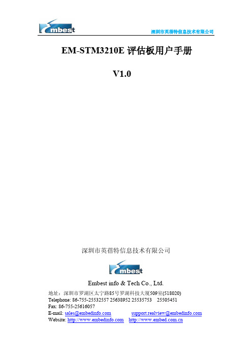
EM-STM3210E评估板用户手册V1.0深圳市英蓓特信息技术有限公司Embest info & Tech Co., Ltd.地址:深圳市罗湖区太宁路85号罗湖科技大厦509室(518020) Telephone: 86-755-25532557 25638952 25535753 25505451Fax: 86-755-25616057E-mail: sales@ support.realview@ Website: 第一章概述EM-STM3210E是英蓓特公司新推出的一款基于ST意法半导体STM32系列处理器(Cortex-M3内核)的全功能评估板。
功能接口丰富,是一个用于应用开发很好的平台,也是学习者的首选。
配合本公司的调试工具ULINK2一起使用,更是为大家提供了一个良好的开发环境,从而为自己的应用开发节省了时间,提高的效率。
EM-STM3210E评估板主要性能:◆处理器:STM32F103ZE,主频:72MHz◆2MB NOR FLASH◆128KB SRAM◆128MB NAND FLASH◆8M byte SPI Flash◆RTC( 带后备电池)◆启动跳线设置◆两路可选电源:5VDC供电,USB供电◆一个SD存储卡接口◆TFT- LCD屏接口◆一个温度传感器◆一路DAC音频输出◆20Pin JTAG调试接口◆2个三线RS232串行口◆一个USB Device接口◆一个具有控制四个方向和确定功能的摇杆手柄◆四个功能按键:Reset,Wakeup,Temper和User按键◆四个Led灯◆四位八段数码管输出◆一个CAN总线接口,通过DB9接口引出◆一路AD输入◆四个26Pin用户扩展接口第二章EM-STM3210E硬件介绍EM-STM3210E功能模块图如下图所示:2.1接口一览表SPI FLASH输入旋钮五维摇杆按键电源跳线选择SPEAKER2.2跳线一览表2.3电源EM-STM3210E评估板有两种供电方式,通过JP5选择以下其中一种方式供电。
LMP7721多功能评估板使用说明1 引言LMP7721评估板提供了一个平台,用来测试LMP7721放大器的性能和输入偏流。
利用芯片内保护驱动器和一个封装外引脚将放大器的输入与电源和输出引脚相隔离,优化LMP7721放大器获得极低的输入偏流,典型值为3fA。
图1为LMP7721评估板。
图1 LMP7721评估板2评估板的清洗2.1清洗材料和工具(1) 新鲜的异丙醇(“外用酒精”或“IPA”)。
(2) 将酸刷子的刷毛修剪至1cm(将刷毛向手柄内推或剪短刷毛)。
(3) 一次性低皮棉湿巾(小号“低尘擦拭纸”)。
(4) 压缩空气(喷雾喷粉罐或空气枪)。
(5) 热风枪,〜200℃(吹风机通常不够热,但可以使用)。
2.2清洗步骤(1) 按正常的清洗程序清洗电路板以消除焊剂、指纹以及其他主要污染物(水洗)。
(2) 用一双钳子或镊子按住板子,缓慢移动板子到热风枪前面一两分钟,以蒸发掉任何剩余的水分(距离喷嘴处不小于5cm)。
(3) 让板子冷却到室温,用新鲜、干净的异丙醇清洗板子且浸泡数秒钟。
(4) 立即用酸刷擦洗电路板,特别是周围区域以及U1引脚和RS焊盘之间。
像“裸露”区域和保护线路区域等关键区域应该清洁、擦洗彻底。
用小毛巾快速擦拭整个板子和吸收掉大部分的多余酒精。
不要忘了电路板的底部也要擦洗。
(5) 用新鲜的酒精再次冲洗以上区域,用一条新的小毛巾快速擦拭过量的酒精。
然后,立即用压缩空气吹干剩余的酒精,不要用水。
水分会在SMT设备下隐藏。
(注:SMT表面组装技术)(6) 吹完板子后,立即用新鲜的小毛巾擦拭以除去残留的任何酒精残留物。
用新的小毛巾擦拭板子顶部和板子底部。
(7) 重复步骤2,用加热枪以消除剩余的多余酒精。
如果有任何白色残留物,重复步骤2。
如果白点依然存在,所用酒精被水污染。
(8) 在不使用时,存放板子在一个密封的容器中。
可以用干燥剂包裹板子。
如果干燥剂不可用,换两汤匙干生米用无尘纸包裹也可。
3防护装置和保护罩防护装置是分微微安培电流设计中的重要概念。
General DescriptionThe DIODES™ AL8863 is a step-down DC-DC controller de-signed to drive LEDs with high output current. The device oper-ates at an input supply voltage from 4.5V to 60V. Series connec-tion of the LEDs provides identical LED currents resulting in uni-form brightness and eliminating the need for ballast resistors. The switching frequency range of AL8863 is from 50kHz to 1MHz. The wide operating frequency range allows more flexibility on compo-nent selection, and also with operating up to 1MHz, it allows the use of smaller size external components, hence minimizing the PCB size and driver board.The output current of AL8863 is set via an external resistor con-nected between the VIN and CSN input pins. Dimming is achieved by applying a PWM signal at the DIM input pin. The soft-start time can be adjusted using an external capacitor from the DIM pin to ground.The AL8863 is available in the thermally enhanced SO-8EP pack-age. Applications∙Commercial & Industrial Lighting∙Architecture Lighting∙External LED Drivers and Smart LightingKey Features∙Wide Input Voltage Range: 4.5V to 60V∙Operating Frequency Range: 50kHz to 1MHz∙1000:1 PWM Dimming Resolution at 100Hz∙Single Pin for On/Off and Brightness Control by PWM Sig-nal∙Fault Status Indication for Abnormal Operation∙LED Shorted Protection∙Inherent Open-Circuit LED Protection∙Programmable Thermal Fold-Back Operation Through NTC Pin∙Overtemperature Shutdown∙Thermally Enhanced SO-8EP Package∙Totally Lead-Free & Fully RoHS CompliantAL8863EV1 SpecificationsEVB Physical PictureFigure 1: Top ViewFigure 2: Bottom Vie wConnection InstructionsPower Supply Input: 5~60VDC (VIN, GND);DIM: Multi-function On/Off and brightness control pin, this pin can be used to achieve dimming and for switching the output current off. Leave floating for normal operation;PWM Signal Input: Remove C15 and connect 0Ω for R6, apply PWM signal to DIM (DIM, GND);Analog Signal Inpu t: A low−pass filtered (R6 and C15) be added, apply analog signal to DIM (DIM, GND);LED A: LED A connects to the external LED anode;LED K: LED K connects to the external LED cathode.Evaluation Board SchematicFigure 3: Evaluation Board SchematicEvaluation Board LayoutFigure 4:PCB Board Layout Top ViewFigure 5:PCB Board Layout Bottom ViewQuick Start Guide1. By default, the evaluation board is preset at 3A LED current by R1, R2 and R3.2. Non-dimming operation: Leave DIM pin floating for normal operation.3. Power Supply: Connect the 5~60VDC to VIN & GND pin to supply the system.4. PWM Dimming: Remove C15, apply a PWM signal (Low level <0.3V, High level >2.6V, transition time less than 1μs) to PWM pin todim the LEDs. The recommended PWM signal frequency is from 100Hz to 20 kHz.5. Analog Dimming: Add a low−pass filtered (R6 and C15) DC signal converted from DC source, the DIM pin can be driven between0.3V and 2.6V adjusting over a wide full range.6. Soft-start: Connect a capacitor (C15) to increase soft-start time.Bill of MaterialNote: The component part numbers are correct at the time of publication. Diodes Inc. reserves the right to substitute other parts where nec-essary, without further notification.Functional WaveformsSwitching waveform(Vin=40V, 6LEDs) (Y-Vin, R-SW, G-DIM, B-I L) Start-up waveform(Vin=40V, 6LEDs) (Y-Vin, R-SW, G-DIM, B-I L)Soft Start waveform (Vin=40V, 6LEDs, C15=100nF) (Y-Vin, R-SW, G-DIM, B-I L) PWM Dimming waveform(Vin=40V, 6LEDs) (PWM frequency=1KHz, Duty=80%)(Y-Vin, R-SW, G-DIM, B-I L)Functional WaveformsPWM Dimming waveform(Vin=40V, 6LEDs) (PWM frequency=1KHz, Duty=50%)(Y-Vin, R-SW, G-DIM, B-I L) PWM Dimming waveform(Vin=40V, 6LEDs) (PWM frequency=1KHz, Duty=20%)(Y-Vin, R-SW, G-DIM, B-I L)LED open protection(Vin=40V, 6LEDs) (Y-V FAULT, R-DIM, G- I L, B-SW) LED short protection(Vin=40V, 6LEDs) (Y-Vin, R-SW, G-V out , B-I L)Functional WaveformsLED short protection_1 (Vin=40V, 6LEDs)(Y-VFAULT, R-SW, G- I L, B-V out) LED open protection_FAULT (Vin=40V, 6LEDs)_start up (Y-VFAULT, R-Vdrive, B-V out)LED short protection_FAULT (Vin=40V, 6LEDs)_start up(Y- V FAULT, R-SW, B- V out)Functional Data CurvesEfficiency vs. Input VoltageLED Current vs. Input VoltageE f f i c i e n c y (%)Vin(V)IL E D (m A )Vin(V)PWM Dimming(Vin=40V, 6LEDs)I L E D (m A )PWM Duty(%)CISPR15 EMI PerformanceFigure 6 presents the EMI performance of the AL8863EV1 EVB at 20V input with 6LEDs load. Conducted emissions are measured over a frequency range of 150 kHz to 30 MHz according to the CISPR 15 low-frequency specification. CISPR15 peak and average limit lines are denoted in red. The blue and black spectra are measured using peak and average detection, respectively.Figure 6: CISPR 15 Conducted Emissions Plot, 150 kHz to 30 MHz,VIN = 40 V, IOUT = 3A, 6LEDsThermal TestFigure 7: Top(Vin=40V, 6LEDs, Burn-in time=60min)Figure 8: Bottom(Vin=40V, 6LEDs, Burn-in time=60min)。
USB单片机CH559的评估板说明版本:V1.51、硬件部分1.1开发板图1.1.3CH558&9MINIEVT图1.1.1CH559EVT图1.1.2CH559MINIEVT1.2开发板主芯片及功能说明(1)、芯片工作电源选择:芯片电压选择,VCC和+5V短接,VDD33悬空,CH559的工作电压选为5V;VCC 和3V3短接,VDD33和3V3短接,CH559工作电压选为3.3V;(2)、评估板电源输入:通过P1电源适配器插口输入8-15V的电压,如图1.1.1的P1口;通过USB直接输入5V电压,如图1.1.1和图1.1.2的USB口;通过VCC和GND插针直接输入5V或者3.3V电压,图1.1.1和图1.1.2都可以通过VCC和GND供电;(3)、复位:C15默认不焊,若焊接则延长复位时间;(4)、TF卡使用SPI方式进行操作,使用时R1需焊接0Ω电阻;(5)、串行Flash使用SPI0操作,使用时R6需焊接0Ω电阻;(6)、LED指示灯连接P4.0~P4.3,引脚输出低电平点亮相应的LED;(7)、P5.4/P5.5支持iRS485数据收发,使用时R16/R18焊20K电阻,R17接120Ω电阻;(8)、外扩RAM物理连接采用直接地址方式,用法参考例程XBUS.C,使用时需短接J4;2、评估板资料包说明来源:搜索CH559文件名:CH559EVT.ZIP资料包:头文件(C、汇编)评估板原理图PCB图例程2.1CH559.uvproj功能:CH559keil4工程文件,头文件、延时函数、串口0初始化等常用函数定义;2.2ADC文件夹功能:ADC中断(查询)方式手动和自动采集,ADC采样时钟设置,电压比较功能函数定义;2.3CHIP_ID文件夹功能:芯片唯一ID号获取函数定义;2.4DataFlash文件夹功能:DataFlash擦除读写函数定义;2.5Encryption文件夹功能:芯片常用加密方法介绍和说明;2.6GPIO文件夹功能:GPIO设置和GPIO中断使用说明;2.7IAP文件夹功能:CH559用户程序跳转至IAP升级演示和说明文档,提供上位机软件和源码;2.8LED_CTRL文件夹功能:CH559LED控制卡演示,支持U盘更新显示内容和掉电数据不丢失;2.9PWM文件夹功能:PWM1&2初始化,PWM占空比设置函数;2.10SPI0文件夹功能:SPI0主机从机模式初始化和数据收发演示,主机操作CH376,从机连接其他C51MCU;2.11SPI1文件夹功能:SPI0主机模式初始化和数据收发演示,主机操作CH376;2.12Timer0文件夹功能:定时器0初始化和定时器、计数器使用函数定义;2.13Timer1文件夹功能:定时器1初始化和定时器、计数器使用函数定义;2.14Timer2文件夹功能:定时器2初始化和定时器、计数器使用函数定义,定时器2捕捉功能函数定义;2.15Timer3文件夹功能:定时器3初始化和定时器、计数器使用函数定义,定时器3捕捉功能函数定义和PWM3设置及使用;2.16UART0文件夹功能:串口0初始化和中断收发示例;2.17WDOG文件夹功能:看门狗初始化和喂狗;2.18XBUS文件夹功能:并行总线初始化和数据收发函数定义;2.19USB_LIB文件夹功能:USB文件系统库;2.20USB文件夹A.DEVICE文件夹模拟USB键鼠例程,支持部分类命令;模拟厂商自定义设备,需要安装CH372驱动,可以通过372test.exe调试(批量数据收发,中断传输);B.HOST文件夹USB主机应用例子,初始化和枚举USB端口连接的设备,支持一级外部HUB,可以操作USB键鼠和HUB,打印机,包含HID类命令处理;C.U_DISK字节方式读写文件,包括文件创建、删除、修改文件属性,修改文件名;扇区方式读写文件,包括文件创建、删除、修改文件属性,修改文件名;创建文件夹和文件创建;枚举根目录或者指定目下的文件;2.21PUB评估板说明功能:评估板说明、评估板原理图3、MCU ISP下载软件说明3.1下载前准备3.1.1ISP变更重要:因为ISP工具升级更新,芯片BOOT版本V2.30以前的版本需要在V2.40及以上版本ISP工具上选择支持的BOOT版本,以下以ISPTool(V2.40)为例,默认支持最新BOOT。