LT6220资料
- 格式:pdf
- 大小:289.04 KB
- 文档页数:20
LT6220/LT6221/LT6222
1sn622012 622012fs–
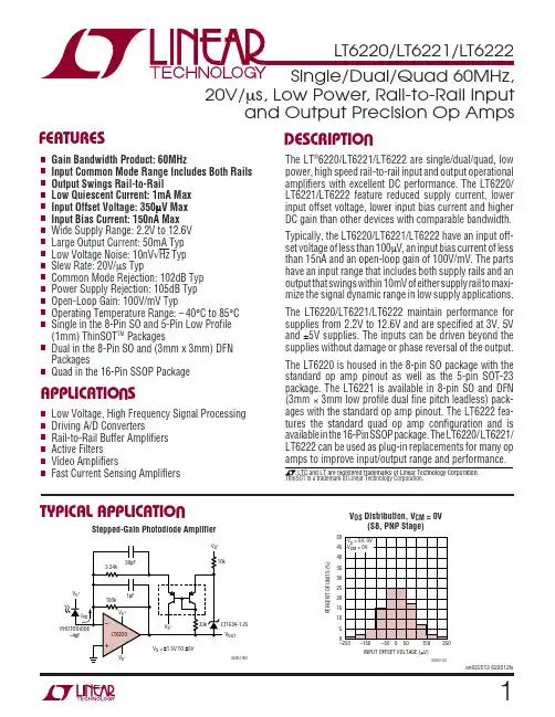
+IPDPHOTODIODE~4pFVS+
VS+VS+
VS–VS–LT6220100k3.24k
33k10k
1pF30pF
LT1634-1.25VOUTVS = ±1.5V TO ±5V622012 TA01■Low Voltage, High Frequency Signal Processing
■Driving A/D Converters
■Rail-to-Rail Buffer Amplifiers■Active Filters
■Video Amplifiers
■Fast Current Sensing Amplifiers■Gain Bandwidth Product: 60MHz■Input Common Mode Range Includes Both Rails
■Output Swings Rail-to-Rail
■Low Quiescent Current: 1mA Max■Input Offset Voltage: 350µV Max
■Input Bias Current: 150nA Max
■Wide Supply Range: 2.2V to 12.6V■Large Output Current: 50mA Typ
■Low Voltage Noise: 10nV√Hz Typ
■Slew Rate: 20V/µs Typ■Common Mode Rejection: 102dB Typ
■Power Supply Rejection: 105dB Typ
■Open-Loop Gain: 100V/mV Typ■Operating Temperature Range: –40°C to 85°C
■Single in the 8-Pin SO and 5-Pin Low Profile(1mm) ThinSOTTM Packages■Dual in the 8-Pin SO and (3mm x 3mm) DFNPackages
■Quad in the 16-Pin SSOP PackageSingle/Dual/Quad 60MHz,
20V/µs, Low Power, Rail-to-Rail Input
and Output Precision Op Amps
The LT®6220/LT6221/LT6222 are single/dual/quad, lowpower, high speed rail-to-rail input and output operationalamplifiers with excellent DC performance. The LT6220/LT6221/LT6222 feature reduced supply current, lowerinput offset voltage, lower input bias current and higherDC gain than other devices with comparable bandwidth.
Typically, the LT6220/LT6221/LT6222 have an input off-set voltage of less than 100µV, an input bias current of lessthan 15nA and an open-loop gain of 100V/mV. The partshave an input range that includes both supply rails and anoutput that swings within 10mV of either supply rail to maxi-mize the signal dynamic range in low supply applications.
The LT6220/LT6221/LT6222 maintain performance forsupplies from 2.2V to 12.6V and are specified at 3V, 5Vand ±5V supplies. The inputs can be driven beyond thesupplies without damage or phase reversal of the output.
The LT6220 is housed in the 8-pin SO package with thestandard op amp pinout as well as the 5-pin SOT-23package. The LT6221 is available in 8-pin SO and DFN(3mm × 3mm low profile dual fine pitch leadless) pack-ages with the standard op amp pinout. The LT6222 fea-tures the standard quad op amp configuration and isavailable in the 16-Pin SSOP package. The LT6220/ LT6221/LT6222 can be used as plug-in replacements for many opamps to improve input/output range and performance.
, LTC and LT are registered trademarks of Linear Technology Corporation.
Stepped-Gain Photodiode AmplifierFEATURESDESCRIPTIOU
APPLICATIO SU
TYPICAL APPLICATIOUThinSOT is a trademark of Linear Technology Corporation.
VOS Distribution, VCM = 0V(S8, PNP Stage)
INPUT OFFSET VOLTAGE (µV)–250PERCENT OF UNITS (%)
304050
150
622012 G0120
10253545
15
50–150–50050250VS = 5V, 0VVCM = 0V元器件交易网www.cecb2b.comLT6220/LT6221/LT6222
2sn622012 622012fsTotal Supply Voltage (VS– to VS+).........................12.6VInput Voltage (Note 2)..............................................±VSInput Current (Note 2)........................................±10mAOutput Short Circuit Duration (Note 3)............IndefiniteOperating Temperature Range (Note 4)...–40°C to 85°CSpecified Temperature Range (Note 5)....–40°C to 85°C
ORDER PARTNUMBERDD PART*MARKINGTJMAX = 125°C, θJA = 160°C/W (NOTE 10)EXPOSED PAD INTERNALLY CONNECTED TO VS–(PCB CONNECTION OPTIONAL)
LT6221CDDLT6221IDDABSOLUTE AXIU RATIGSWWWU
PACKAGE/ORDER IFORATIOUUW(Note 1)
Consult LTC Marketing for parts specified with wider operating temperature ranges.*The temperature grades are identified by a label on the shipping container.Maximum Junction Temperature..........................150°C(DD Package)...................................................125°CStorage Temperature.............................–65°C to 150°C(DD Package)....................................–65°C to 125°CLead Temperature (Soldering, 10 sec.).................300°C
TOP VIEW
DD PACKAGE8-LEAD (3mm × 3mm) PLASTIC DFN5678
4321OUT A–IN A+IN AVS–VS+OUT B–IN B+IN BABTOP VIEW
GN PACKAGE16-LEAD NARROW PLASTIC SSOP12345678161514131211109OUT A–IN A+IN AVS+
+IN B–IN BOUT BNCOUT D–IN D+IN DVS–+IN C–IN COUT CNCA
BCD
TJMAX = 150°C, θJA = 135°C/WTJMAX = 150°C, θJA = 190°C/W
ORDER PARTNUMBERS8 PARTMARKINGORDER PARTNUMBERSSOP PARTMARKING
LT6221CS8LT6221IS8LT6222CGNLT6222IGNLADZ62226222I62216221IORDER PARTNUMBERORDER PARTNUMBER
S5 PART*MARKINGS8 PARTMARKING
TJMAX = 150°C, θJA = 190°C/WTJMAX = 150°C, θJA = 250°C/W (NOTE 10)12348765TOP VIEW
OUT A–IN A+IN AVS–VS+OUT B–IN B+IN B
S8 PACKAGE8-LEAD PLASTIC SOAB5 VS+
4 –INVOUT 1TOP VIEW
S5 PACKAGE5-LEAD PLASTIC TSOT-23VS– 2+IN 3+–LT6220CS8LT6220IS8
62206220ILT6220CS5LT6220IS5
LTAFP
12348765TOP VIEW
NC–IN+INVS–NCVS+
VOUTNC
S8 PACKAGE8-LEAD PLASTIC SO+–元器件交易网www.cecb2b.com