HT48R06A-1 HT48C06 8位经济型输入
- 格式:pdf
- 大小:488.67 KB
- 文档页数:34


HT48R06A-18-Bit OTP Microcontroller1February 25,2000General DescriptionThe device is an 8-bit high performance RISC-like microcontroller designed for multi-ple I/O product applications.The device is par-ticularly suitable for use in products such as remote controllers,fan/light controllers,wash-ing machine controllers,scales,toys and vari-ous subsystem controllers.A halt feature is included to reduce power consumption.The program and option memories can be elec-trically programmed,making the microcontrol-ler suitable for use in product development.Features·Operating voltage:f SYS =4MHz:3.3V~5.5V f SYS =8MHz:4.5V~5.5V ·13bidirectional I/O lines·An interrupt input shared with an I/O line ·8-bit programmable timer/event counter with overflow interrupt and 8-stage prescaler ·On-chip crystal and RC oscillator ·Watchdog timer·1024´14program memory PROM ·64´8data memory RAM·Buzzer driving pair and PFD supported·Halt function and wake-up feature reduce power consumption·Up to 0.5m s instruction cycle with 8MHz system clock at V DD =5V·Allinstructionsinoneortwomachinecycles ·14-bit table read instruction ·Two-level subroutine nesting ·Bit manipulation instruction ·63powerful instructions ·Low voltage reset function ·18-pin DIP/SOP packagePreliminary查询HT48R06A-1供应商捷多邦,专业PCB打样工厂,24小时加急出货Block DiagramPin Assignment2February25,2000Pin DescriptionPin No.Pin Name I/O ROM CodeOption Description4~118~15PA0~PA7I/O Pull-high*Wake-upBidirectional8-bit input/output port.Each bit can beconfigured as wake-up input by ROM code option.Software instructions determine the CMOS output orschmitt trigger input with a pull-high resistor(deter-mined by pull-high options).7 6 5PB0/BZPB1/BZPB2I/OPull-high*I/O orBZ/BZBidirectional3-bit input/output port.Software in-structions determine the CMOS output or schmitttrigger input with a pull-high resistor(determined bypull-high options).The PB0and PB1are pin-shared with the BZ and BZ,respectively.Once the PB0and PB1are selected asbuzzer driving outputs,the output signals come froman internal PFD generator(shared with timer/eventcounter).8VSS¾¾Negative power supply,ground9 10PC0/INTPC1/TMR I/O Pull-high*Bidirectional I/O lines.Software instructions deter-mine the CMOS output or SCHMITT trigger inputwith a pull-high resistor(determined by pull-high op-tions).The external interrupt and timer input arepin-shared with the PC0and PC1,respectively.Theexternal interrupt input is activated on a high to lowtransition.11RES I¾Schmitt trigger reset input.Active low 12VDD¾¾Positive power supply13 14OSC1OSC2IOCrystalor RCOSC1,OSC2are connected to an RC network or Crys-tal(determined by ROM code option)for the internalsystem clock.In the case of RC operation,OSC2is theoutput terminal for1/4system clock.*All pull-high resistors are controlled by an option bit.Absolute Maximum RatingsSupply Voltage...............V SS-0.3V to V SS+5.5V Storage Temperature.................-50°C to125°C Input Voltage.................V SS-0.3V to V DD+0.3V Operating Temperature..............-40°C to85°CNote:These are stress ratings only.Stresses exceeding the range specified under"Absolute Maxi-mum Ratings"may cause substantial damage to the device.Functional operation of this device at other conditions beyond those listed in the specification is not implied and prolonged expo-sure to extreme conditions may affect device reliability.3February25,2000D.C.Characteristics Ta=25°CSymbol ParameterTest ConditionsMin.Typ.Max.Unit V DD ConditionsV DD1Operating Voltage¾f SYS=4MHz 3.3¾ 5.5V V DD2Operating Voltage¾f SYS=8MHz 4.5¾ 5.5VI DD1Operating Current(Crystal OSC)3.3VNo load,f SYS=4MHz¾12mA 5V¾24mAI DD2Operating Current(RC OSC)3.3VNo load,f SYS=4MHz¾12mA 5V¾24mAI DD3Operating Current(Crystal OSC)5V No load,fsys=8MHz¾510mAI STB1Standby Current(WDT Enabled)3.3VNo load,system Halt¾¾5m A 5V¾¾10m AI STB2Standby Current(WDT Disabled)3.3VNo load,system Halt¾¾1m A 5V¾¾2m AV IL1Input Low Voltage forI/O Ports,TMR and INT 3.3V¾0¾0.2V DD V 5V¾0¾0.2V DD VV IH1Input High Voltage forI/O Ports,TMR and INT 3.3V¾0.8V DD¾V DD V 5V¾0.8V DD¾V DD VV IL3Input Low Voltage(RES)3.3V¾0¾0.4V DD V 5V¾0¾0.4V DD VV IH3Input High Voltage(RES)3.3V¾0.9V DD¾V DD V 5V¾0.9V DD¾V DD VV LVR Low Voltage Reset¾¾ 3.1 3.2 3.3VI OL I/O Port Sink Current 3.3V V OL=0.1V DD48¾mA 5V V OL=0.1V DD1020¾mAI OH I/O Port SourceCurrent 3.3V V OH=0.9V DD-2-4¾mA 5V V OH=0.9V DD-5-10¾mAR PH Pull-high Resistance 3.3V¾406080k W 5V¾103050k W4February25,2000A.C.Characteristics Ta=25°CSymbol ParameterTest ConditionsMin.Typ.Max.Unit V DD Conditionsf SYS1System Clock(Crystal OSC)3.3V¾400¾4000kHz 5V¾400¾8000kHzf SYS2System Clock(RC OSC)3.3V¾400¾4000kHz 5V¾400¾4000kHzf TIMER Timer I/P Frequency(TMR)3.3V¾0¾4000kHz 5V¾0¾4000kHzt WDTOSC Watchdog Oscillator 3.3V¾4386168m s 5V¾3565130m st WDT1Watchdog Time-out Period(RC)3.3V Without WDTprescaler112243ms 5V91735mst WDT2Watchdog Time-out Period(System Clock)¾Without WDTprescaler¾1024¾t SYSt RES External Reset Low PulseWidth¾¾1¾¾m st SST System Start-up TimerPeriod¾Power-up,reset orwake-up from Halt¾1024¾t SYSt INT Interrupt Pulse Width¾¾1¾¾m s5February25,2000Functional DescriptionExecution flowThe system clock for the microcontroller is de-rived from either a crystal or an RC oscillator. The system clock is internally divided into four non-overlapping clocks.One instruction cycle consists of four system clock cycles. Instruction fetching and execution are pipelined in such a way that a fetch takes an in-struction cycle while decoding and execution takes the next instruction cycle.However,the pipelining scheme causes each instruction to ef-fectively execute in a cycle.If an instruction changes the program counter,two cycles are re-quired to complete the instruction.Program counter-PCThe program counter(PC)controls the se-quence in which the instructions stored in pro-gram PROM are executed and its contents specify full range of program memory.After accessing a program memory word to fetch an instruction code,the contents of the program counter are incremented by one.The program counter then points to the memory word contain-ing the next instruction code.When executing a jump instruction,conditional skip execution,loading PCL register,subrou-tine call,initial reset,internal interrupt,exter-nal interrupt or return from subroutine,the PC manipulates the program transfer by loading the address corresponding to each instruction. The conditional skip is activated by instruc-tions.Once the condition is met,the next in-struction,fetched during the current instruction execution,is discarded and a dummy cycle replaces it to get the proper in-struction.Otherwise proceed with the next in-struction.The lower byte of the program counter(PCL)is a readable and writable register(06H).Moving data into the PCL performs a short jump.The destination will be within256locations. When a control transfer takes place,an addi-tional dummy cycle is required.Program memory-PROMThe program memory is used to store the pro-gram instructions which are to be executed.It also contains data,table,and interrupt entries, and is organized into1024´14bits,addressed by the program counter and table pointer.Execution flow6February25,2000Certain locations in the program memory are reserved for special usage:·Location000HThis area is reserved for program initializa-tion.After chip reset,the program always be-gins execution at location000H.·Location004HThis area is reserved for the external inter-rupt service program.If the INT input pin is activated,the interrupt is enabled and the stack is not full,the program begins execution at location004H.·Location008HThis area is reserved for the timer/event coun-ter interrupt service program.If a timer inter-rupt results from a timer/event counteroverflow,and if the interrupt is enabled and the stack is not full,the program begins execution at location008H.·Table locationAny location in the PROM space can be used as look-up tables.The instructions"TABRDC [m]"(the current page,1page=256words) and"TABRDL[m]"(the last page)transfer the contents of the lower-order byte to the specified data memory,and the higher-order byte to TBLH(08H).Only the destination of the lower-order byte in the table is well-defined,the other bits of the table word are transferred to the lower portion of TBLH, and the remaining2bits are read as"0".The Table Higher-order byte register(TBLH)is read only.The table pointer(TBLP)is a read/write register(07H),which indicates the table location.Before accessing the table,the location must be placed in TBLP.The TBLH is read only and cannot be restored.If the main routine and the ISR(Interrupt ServiceModeProgram Counter*9*8*7*6*5*4*3*2*1*0Initial Reset0000000000 External Interrupt0000000100 Timer/Event Counter Overflow0000001000 Skip PC+2Loading PCL*9*8@7@6@5@4@3@2@1@0 Jump,Call Branch#9#8#7#6#5#4#3#2#1#0 Return from Subroutine S9S8S7S6S5S4S3S2S1S0Program counterNote:*9~*0:Program counter bits S9~S0:Stack register bits#9~#0:Instruction code bits@7~@0:PCL bitsProgram memory7February25,20008February 25,2000Instruction Table Location*9*8*7*6*5*4*3*2*1*0TABRDC [m]P9P8@7@6@5@4@3@2@1@0TABRDL [m]11@7@6@5@4@3@2@1@0Table locationNote:*9~*0:Table location bitsP9,P8:Current program counter bits@7~@0:Table pointer bitsRoutine)both employ the table read instruc-tion,the contents of the TBLH in the main routine are likely to be changed by the table read instruction used in the ISR.Errors can occur.In other words,using the table read in-struction in the main routine and the ISR si-multaneously should be avoided.However,if the table read instruction has to be applied in both the main routine and the ISR,the inter-rupt is supposed to be disabled prior to the ta-ble read instruction.It will not be enabled until the TBLH has been backed up.All table related instructions require two cycles to com-plete the operation.These areas may function as normal program memory depending upon the requirements.Stack register -STACKThis is a special part of the memory which is used to save the contents of the program coun-ter (PC)only.The stack is organized into 2lev-els and is neither part of the data nor part of the program space,and is neither readable nor writable.The activated level is indexed by the stack pointer (SP)and is neither readable nor writeable.At a subroutine call or interrupt ac-knowledgment,the contents of the program counter are pushed onto the stack.At the end of a subroutine or an interrupt routine,signaled by a return instruction (RET or RETI),the pro-gram counter is restored to its previous value from the stack.After a chip reset,the SP will point to the top of the stack.If the stack is full and a non-masked interrupt takes place,the interrupt request flag will be recorded but the acknowledgment will be inhib-ited.When the stack pointer is decremented (by RET or RETI),the interrupt will be serviced.This feature prevents stack overflow allowing the programmer to use the structure more eas-ily.In a similar case,if the stack is full and a "CALL"is subsequently executed,stack over-flow occurs and the first entry will be lost (only the most recent 2return addresses are stored).Data memory -RAMThe data memory is designed with 81´8bits.The data memory is divided into two func-tional groups:special function registers and general purpose data memory (64´8).Most are read/write,but some are read only.The special function registers include the indi-rect addressing register (00H),timer/event counter (TMR;0DH),timer/event counter con-trol register (TMRC;0EH),program counter lower-order byte register (PCL;06H),memory pointer register (MP;01H),accumulator (ACC;05H),table pointer (TBLP;07H),table higher-order byte register (TBLH;08H),status register (STATUS;0AH),interrupt control reg-ister (INTC;0BH),watchdog timer option set-ting register (WDTS;09H),I/O registers (PA;12H,PB;14H,PC;16H)and I/O control registers (PAC;13H,PBC;15H,PCC;17H).The remaining space before the 40H is reserved for future expanded usage and reading these loca-tions will get "00H".The general purpose data memory,addressed from 40H to 7FH,is used for data and control information under in-struction commands.All of the data memory areas can handle arith-metic,logic,increment,decrement and rotate operations directly.Except for some dedicated bits,each bit in the data memory can be set and reset by"SET[m].i"and"CLR[m].i".They are also indirectly accessible through memory pointer register(MP;01H).Indirect addressing registerLocation00H is an indirect addressing register that is not physically implemented.Any read/write operation of[00H]accesses data mem-ory pointed to by MP(01H).Reading location00H itself indirectly will return the result00H.Writ-ing indirectly results in no operation.The memory pointer register MP(01H)is a7-bit register.The bit7of MP is undefined and reading will return the result1.Any writing operation to MP will only transfer the lower7-bit data to MP.AccumulatorThe accumulator is closely related to ALU oper-ations.It is also mapped to location05H of the data memory and can carry out immediate data operations.The data movement between two data memory locations must pass through the accumulator.Arithmetic and logic unit-ALUThis circuit performs8-bit arithmetic and logic operations.The ALU provides the following func-tions:Arithmetic operations(ADD,ADC,SUB,SBC, DAA)·Logic operations(AND,OR,XOR,CPL)Rota-tion(RL,RR,RLC,RRC)·Increment and Decrement(INC,DEC)·Branch decision(SZ,SNZ,SIZ,SDZ....) The ALU not only saves the results of a data op-eration but also changes the status register. Status register-STATUSThis8-bit register(0AH)contains the zero flag (Z),carry flag(C),auxiliary carry flag(AC), overflow flag(OV),power down flag(PD),andwatchdog time-out flag(TO).It also records the status information and controls the operation sequence.With the exception of the TO and PD flags, bits in the status register can be altered by instructions like most other registers.Any data written into the status register will not change the TO or PD flag.In addition opera-RAM mapping9February25,2000tions related to the status register may give different results from those intended.The TO flag can be affected only by system power-up,a WDT time-out or executing the "CLR WDT"or"HALT"instruction.The PD flag can be affected only by executing the "HALT"or"CLR WDT"instruction or a sys-tem power-up.The Z,OV,AC and C flags generally reflect the status of the latest operations.In addition,on entering the interrupt sequence or executing the subroutine call,the status reg-ister will not be pushed onto the stack automat-ically.If the contents of the status are important and if the subroutine can corrupt the status register,precautions must be taken to save it properly.InterruptThe device provides an external interrupt and internal timer/event counter interrupts.The Interrupt Control Register(INTC;0BH)con-tains the interrupt control bits to set the en-able/disable and the interrupt request flags. Once an interrupt subroutine is serviced,all the other interrupts will be blocked(by clearing the EMI bit).This scheme may prevent any fur-ther interrupt nesting.Other interrupt re-quests may happen during this interval but only the interrupt request flag is recorded.If a certain interrupt requires servicing within the service routine,the EMI bit and the correspond-ing bit of INTC may be set to allow interrupt nesting.If the stack is full,the interrupt request will not be acknowledged,even if the related in-terrupt is enabled,until the SP is decremented. If immediate service is desired,the stack must be prevented from becoming full.All these kinds of interrupts have a wake-up ca-pability.As an interrupt is serviced,a control transfer occurs by pushing the program counter onto the stack,followed by a branch to a sub-routine at specified location in the program memory.Only the program counter is pushed onto the stack.If the contents of the register or status register(STATUS)are altered by the in-terrupt service program which corrupts the de-sired control sequence,the contents should be saved in advance.External interrupts are triggered by a high to low transition of INT and the related interruptLabels Bits FunctionC0C is set if the operation results in a carry during an addition operation or if a bor-row does not take place during a subtraction operation;otherwise C is cleared.C is also affected by a rotate through carry instruction.AC1AC is set if the operation results in a carry out of the low nibbles in addition or no borrow from the high nibble into the low nibble in subtraction;otherwise AC is cleared.Z2Z is set if the result of an arithmetic or logic operation is zero;otherwise Z is cleared.OV3OV is set if the operation results in a carry into the highest-order bit but not a carry out of the highest-order bit,or vice versa;otherwise OV is cleared.PD4PD is cleared by system power-up or executing the"CLR WDT"instruction.PD is set by executing the"HALT"instruction.TO5TO is cleared by system power-up or executing the"CLR WDT"or"HALT"in-struction.TO is set by a WDT time-out.¾6Undefined,read as"0"¾7Undefined,read as"0"Status register10February25,2000request flag(EIF;bit4of INTC)will be set. When the interrupt is enabled,the stack is not full and the external interrupt is active,a sub-routine call to location04H will occur.The in-terrupt request flag(EIF)and EMI bits will be cleared to disable other interrupts.The internal timer/event counter interrupt is initialized by setting the timer/event counter interrupt request flag(TF;bit5of INTC), caused by a timer overflow.When the interrupt is enabled,the stack is not full and the TF bit is set,a subroutine call to location08H will occur. The related interrupt request flag(TF)will be reset and the EMI bit cleared to disable further interrupts.During the execution of an interrupt subroutine, other interrupt acknowledgments are held until the"RETI"instruction is executed or the EMI bit and the related interrupt control bit are set to 1(of course,if the stack is not full).To return from the interrupt subroutine,"RET"or"RETI" may be invoked.RETI will set the EMI bit to en-able an interrupt service,but RET will not. Interrupts,occurring in the interval between the rising edges of two consecutive T2pulses, will be serviced on the latter of the two T2 pulses,if the corresponding interrupts are en-abled.In the case of simultaneous requests the following table shows the priority that is ap-plied.These can be masked by resetting the EMI bit.No.Interrupt Source Priority Vectora External Interrupt104Hb Timer/eventCounter Overflow208H The timer/event counter interrupt request flag (TF),external interrupt request flag(EIF),en-able timer/event counter bit(ETI),enable ex-ternal interrupt bit(EEI)and enable master interrupt bit(EMI)constitute an interrupt con-trol register(INTC)which is located at0BH in the data memory.EMI,EEI,ETI are used to control the enabling/disabling of interrupts. These bits prevent the requested interrupt from being serviced.Once the interrupt request flags(TF,EIF)are set,they will remain in the INTC register until the interrupts are serviced or cleared by a software instruction.It is recommended that a program does not use the"CALL subroutine"within the inter-rupt subroutine.Interrupts often occur in an unpredictable manner or need to be serviced immediately in some applications.If only one stack is left and enabling the interrupt is not well controlled,the original control sequence willRegister Bit bel FunctionINTC (0BH)0EMI Controls the master(global)interrupt(1=enabled;0=disabled)1EEI Controls the external interrupt(1=enabled;0=disabled)2ETI Controls the timer/event counter interrupt(1=enabled;0=disabled)3¾Unused bit,read as"0"4EIF External interrupt request flag(1=active;0=inactive)5TF Internal timer/event counter request flag(1=active;0=inactive)6¾Unused bit,read as"0"7¾Unused bit,read as"0"INTC register11February25,2000be damaged once the"CALL"operates in the in-terrupt subroutine.Oscillator configurationThere are two oscillator circuits in the microcontroller.Both are designed for system clocks,namely the RC oscillator and the Crystal oscillator, which are determined by the ROM code option. No matter what oscillator type is selected,the signal provides the system clock.The HALT mode stops the system oscillator and ignores an external signal to conserve power.If an RC oscillator is used,an external resistor between OSC1and VDD is required and the resistance must range from51k W to1M W.The system clock,divided by4,is available on OSC2,which can be used to synchronize exter-nal logic.The RC oscillator provides the most cost effective solution.However,the frequency of oscillation may vary with VDD,tempera-tures and the chip itself due to process varia-tions.It is,therefore,not suitable for timing sensitive operations where an accurate oscilla-tor frequency is desired.If the Crystal oscillator is used,a crystal across OSC1and OSC2is needed to provide the feed-back and phase shift required for the oscillator, and no other external components are required. Instead of a crystal,a resonator can also be con-nected between OSC1and OSC2to get a fre-quency reference,but two external capacitors in OSC1and OSC2are required(If the oscillat-ing frequency is less than1MHz).The WDT oscillator is a free running on-chip RC oscillator,and no external components are re-quired.Even if the system enters the power down mode,the system clock is stopped,but the WDT oscillator still works with a period of approxi-mately65m s/5V.The WDT oscillator can be dis-abled by ROM code option to conserve power.Watchdog timer-WDTThe clock source of WDT is implemented by a dedicated RC oscillator(WDT oscillator)or in-struction clock(system clock divided by4),de-cided by ROM code option.This timer is designed to prevent a software malfunction or sequence from jumping to an unknown location with unpredictable results.The watchdog timer can be disabled by a ROM code option.If the watchdog timer is disabled,all the execu-tions related to the WDT result in no operation. Once the internal WDT oscillator(RC oscillator with a period of65m s/5V normally)is selected,it is first divided by256(8-stage)to get the nomi-nal time-out period of approximately 16.6ms/5V.This time-out period may vary with temperatures,VDD and process variations.By invoking the WDT prescaler,longer time-out periods can be realized.Writing data to WS2, WS1,WS0(bit2,1,0of the WDTS)can give differ-ent time-out periods.If WS2,WS1,and WS0are all equal to1,the division ratio is up to1:128,andSystem oscillatorWatchdog timer12February25,2000the maximum time-out period is2.2s/5V seconds. If the WDT oscillator is disabled,the WDT clock may still come from the instruction clock and op-erate in the same manner except that in the HALT state the WDT may stop counting and lose its protecting purpose.In this situation the logic can only be restarted by external logic.The high nibble and bit3of the WDTS are reserved for user's defined flags,which can be used to indicate some specified status.If the device operates in a noisy environment,us-ing the on-chip RC oscillator(WDT OSC)is strongly recommended,since the HALT will stop the system clock.WS2WS1WS0Division Ratio0001:10011:20101:40111:81001:161011:321101:641111:128WDTS registerThe WDT overflow under normal operation will initialize"chip reset"and set the status bit "TO".But in the HALT mode,the overflow will initialize a²warm reset²,and only the PC and SP are reset to zero.To clear the contents of WDT(including the WDT prescaler),three methods are adopted;external reset(a low level to RES),software instruction and a"HALT"in-struction.The software instruction include "CLR WDT"and the other set-"CLR WDT1" and"CLR WDT2".Of these two types of instruc-tion,only one can be active depending on the ROM code option-"CLR WDT times selection option".If the"CLR WDT"is selected(i.e. CLRWDT times equal one),any execution of the"CLR WDT"instruction will clear the WDT. In the case that"CLR WDT1"and"CLR WDT2" are chosen(i.e.CLRWDT times equal two), these two instructions must be executed to clear the WDT;otherwise,the WDT may reset the chip as a result of time-out.Power down operation-HALTThe HALT mode is initialized by the"HALT"in-struction and results in the following...·The system oscillator will be turned off butthe WDT oscillator keeps running(if theWDT oscillator is selected).·The contents of the on chip RAM and regis-ters remain unchanged.·WDT and WDT prescaler will be cleared andrecounted again(if the WDT clock is from theWDT oscillator).·AlloftheI/Oportsmaintaintheiroriginalstatus.·The PD flag is set and the TO flag is cleared.The system can leave the HALT mode by means of an external reset,an interrupt,an external falling edge signal on port A or a WDT overflow.An external reset causes a device initialization and the WDT overflow performs a"warm re-set".After the TO and PD flags are examined, the reason for chip reset can be determined.The PD flag is cleared by system power-up or executing the"CLR WDT"instruction and is set when executing the"HALT"instruction.The TO flag is set if the WDT time-out occurs,and causes a wake-up that only resets the PC and SP;the others keep their original status.The port A wake-up and interrupt methods can be considered as a continuation of normal exe-cution.Each bit in port A can be independently selected to wake up the device by the ROM code option.Awakening from an I/O port stimulus, the program will resume execution of the next instruction.If it is awakening from an inter-rupt,two sequences may happen.If the related interrupt is disabled or the interrupt is enabled but the stack is full,the program will resume execution at the next instruction.If the inter-rupt is enabled and the stack is not full,the reg-ular interrupt response takes place.If an interrupt request flag is set to"1"before enter-ing the HALT mode,the wake-up function of the related interrupt will be disabled.Once a wake-up event occurs,it takes1024t SYS(sys-tem clock period)to resume normal operation.In other words,a dummy period will be inserted after wake-up.If the wake-up results from an interrupt acknowledgment,the actual inter-rupt subroutine execution will be delayed by one or more cycles.If the wake-up results in the13February25,2000。
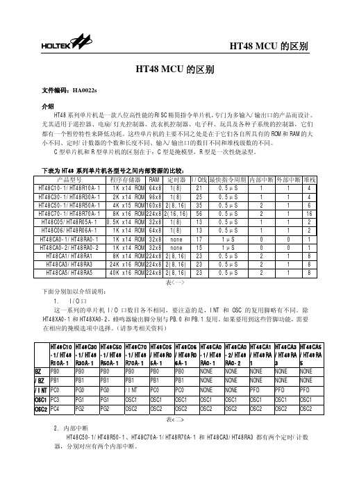
HT48 MCU的区别文件编码:HA0022s介绍HT48系列单片机是一款八位高性能的RISC精简指令单片机,专门为多输入/输出口的产品而设计。
尤其适用于遥控器、电扇/灯光控制器、洗衣机控制器、电子秤、玩具及各种子系统的控制器,它们都有一个暂停特性来降低功耗。
这些单片机的主要不同之处是在于它们各自所具有的ROM和RAM的大小不同、定时/计数器的个数和长度不同、输入/输出口的数目不同和堆栈级数的不同。
C型单片机和R型单片机的区别在于:C型是掩模型,R型是一次性烧录型。
下表为HT48系列单片机各型号之间内部资源的比较:产品型号程序存储器 RAM定时器I/O线最快指令周期内部中断外部中断堆栈HT48C10-1/HT48R10A-1 1K x14 ROM 64x81(8) 21 0.5μS 1 1 4 HT48C30-1/HT48R30A-1 2K x14 ROM 96x81(8) 25 0.5μS 1 1 4 HT48C50-1/HT48R50A-1 4K x15 ROM 160x82(8,16)35 0.5μS 2 1 6 HT48C70-1/HT48R70A-1 8K x16 ROM 224x82(16,16)56 0.5μS 2 116 HT48C05/HT48R05A-1 0.5K x14 ROM 32x81(8) 13 0.5μS 1 1 2 HT48C06/HT48R06A-1 1K x14 ROM 64x81(8) 13 0.5μS 1 1 2 HT48CA0-1/HT48RA0-1 1K x14 ROM 32x8none 17 1μS 0 01 HT48CA0-2/HT48RA0-2 1K x14 ROM 32x8none 15 1μS 0 01 HT48CA1/HT48RA1 8K x14 ROM 224x82(8,16)23 0.5μS2 1 8 HT48CA3/HT48RA3 24K x16 ROM 224x82(8,16)23 0.5μS 2 1 8 HT48CA5/HT48RA5 40K x16 ROM 224x82(8,16)23 0.5μS 2 1 8表<一>下面分别加以介绍说明:1. I/O口这一系列的单片机I/O口数目各不相同,要注意的是,INT和OSC的复用脚略有不同。
1HT48R062在带温度侦测简易型在带温度侦测简易型 充电器中的应用充电器中的应用文件编码:HA0144S简介本范例以HT48R062 8-Bit MCU 为控制核心制作Charger DemoBoard 。
MCU 使用RC 振荡,10小时内误差为30分钟内,具有温度探测功能,当温度过高时自动停止充电。
HT48R062特征简介HT48R062是一种非常低价位的MCU ,其基本特征如下:• HT48R062工作电压,在f SYS =4MHz 时为:2.2V~5.5V ;在f SYS =8MHz 时为:3.3V~5.5V • 11个双向I/O 口• 内建晶体振荡电路和RC 振荡电路 • 内建WATCHDOG TIMER • 内建低电压RESET 电路 • 1Kx14程序内存 • 32x8数据存储器• HALT function and wake-up feature reduce power consumption2硬件方块图及说明• 主控芯片为HT48R062• MCU 通过PA0和PA1检测电池是否装入电池盒 • MCU 通过PB0和PB1来控制是否对电池进行充电•MCU 通过PA3~PA7组成两路温度探测电路,其中PA3控制标准电阻的充放;PA4、PA6控制热敏电阻的充电;PA5、PA7用于读取充电时间• MCU 通过PB2输出一个周期为16ms 的方波,用于进行MCU 工作频率的校正硬件电路简介• P1输入为DC 9V,经C7和C3滤波后送入7805的1脚,7805的3脚的输出为DC 5V。
• C1、C4、C5、R1和R2组成MCU的RESET电路;C2和R3为MCU的RC振荡电路。
• PA0和PA1为输入脚,直接接电池的正极,当没有电池接入时,由于提升电阻的作用输入为高准位;当电池接入时,其对应的PA脚输入的电压为电池电压(一般小于1.5V),因为IO口低准位的范围为0~0.3V DD,由于MCU的V DD为5V,此时PA输入将被读到低准位。