准谐振反激变压器设计
- 格式:xls
- 大小:69.00 KB
- 文档页数:2
反激变压器设计实例设计一个反激变压器是一个非常复杂的工程,需要考虑许多因素,包括输入电压、输出电压、功率需求、电流负载、转换效率等。
在这里,我将给出一个反激变压器的设计实例,以帮助你更好地理解。
假设我们需要设计一个输入电压为220V,输出电压为12V的反激变压器,功率需求为60W。
首先,我们需要确定变压器的转换比。
转换比可以通过输出电压和输入电压的比值来确定。
在本例中,转换比为12V/220V,即0.0545接下来,我们需要确定主电压边(Primary Side)的匝数。
主电压边上的匝数决定了变压器的转化比。
然后,我们需要确定次电压边(Secondary Side)的匝数。
次电压边的匝数通过主电压边的匝数和转换比来计算。
在本例中,次电压边的匝数为1000*0.0545,约为54.5、为了简化设计,可以选择将次电压边的匝数设定为55接下来,我们需要根据功率需求来确定变压器的尺寸。
功率可以通过输入电压和电流来计算。
在本例中,输入电压为220V,功率为60W,那么电流为60W/220V,约为0.27A。
然后,我们可以根据电流负载来确定导线截面积。
在本例中,电流为0.27A,我们可以选择导线截面积为0.5mm²。
接下来,我们需要计算主电压边的绕线长度。
主电压边的绕线长度可以通过主电压边的匝数和导线的长度来计算。
在本例中,主电压边的匝数为1000,并且我们选择导线长度为2m,那么主电压边的绕线长度为1000*2m,约为2000m。
然后,我们需要计算次电压边的绕线长度。
次电压边的绕线长度可以通过次电压边的匝数和导线的长度来计算。
在本例中,次电压边的匝数为55,并且我们选择导线长度为2m,那么次电压边的绕线长度为55*2m,约为110m。
接下来,我们需要计算变压器的转换效率。
转换效率可以通过输出功率和输入功率来计算。
在本例中,输出功率为60W,输入功率可以通过输入电压和电流来计算,即220V*0.27A,约为59.4W。
反激式开关电源变压器设计反激式变压器是反激式开关电源的核心,它决定了反激式变换器一系列的重要参数,如占空比D ,最大峰值电流,设计反激式变压器,就是要让反激式开关电源工作在一个合理的工作点上。
这样可以让其发热量尽量小,对器件的磨损也尽量小。
同样的芯片,同样的磁芯,若是变压器设计不合理,则整个开关电源性能会有很大的下降,如损耗会加大,最大输出功率会下降.设计变压器,就是要先选定一个工作点,在这个点就是最低的交流输入电压,对应于最大的输出功率。
第一步,选定原边感应电压V OR 。
这个值是有自己来设定的,这个值就决定了电源的占空比.可能朋友们不理解什么是原边感应电压。
我们分析一个工作原理图。
当开关管开通的时候,原边相当于一个电感,电感两端加上电压,其电流值不会突变,而线性上升:I 升=Vs*Ton/L 。
这三项分别是原边输入电压,开关开通时间和原边电感量。
在开关管关断的时候,原边电感放电,电感电流会下降,此时有下降了的电流:I 降=V OR *T OFF /L 。
这三项分别是原边感应电压(即放电电压)、开关管管段时间和电感量。
经过一个周期后,原边电感电流会回到原来的值,不可能会变,所以有:Vs *T ON /L=V OR *T OFF /L 。
即上升了的等于下降了的。
上式中用D 来代替T ON ,用(1-D )来代替T OFF .移项可得:D=V OR /(V OR +Vs)。
这就是最大占空比了.比如说我设计的这个变压器,我选定电感电压V OR =20V ,则Vs 为24V ,D=20/(20+24)=0。
455。
第二步,确定原边电流波形的参数原边电流波形有三个参数,平均电流,有效值电流,峰值电流,首先要知道原边电流的波形,原边电流的波形如下。
这是一个梯形波横向表示时间,总想表示电流大小,这个波形有三个值,一个是平均值I 平均,二是有效值I ,三是峰值Ip 。
首先要确定平均值I 平均:I 平均=Po/(η*Vs )。

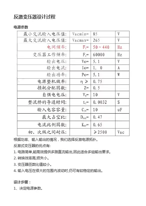
反激变压器设计过程电源参数根据功率、输入输出的情况,我们选择反激电源拓扑。
反激式变压器的优点有:1. 电路简单,能高效提供多路直流输出,因此适合多组输出要求。
2. 转换效率高,损失小。
3. 变压器匝数比值较小。
4. 输入电压在很大的范围内波动时,仍可有较稳定的输出。
设计步骤:1、决定电源参数。
2、计算电路参数。
3、选择磁芯材料。
4、选择磁芯的形状和尺寸。
5、计算变压器匝数、有效气隙电感系数及气隙长度。
6、选择绕组线圈线径。
7、计算变压器损耗和温升。
原理图步骤一、确定电源参数:(有些参数为指标给定,有些参数从资料查得)注:电流比例因数:纹波比例,在重载和低收入情况下的纹波电流和实际电流的比例。
步骤二、计算电路参数:最低直流输入电压:Z为损耗分配因数,如果Z=1.0表示所有损耗都在副边,如果Z=0表示所有的损耗都在原边,在这里取Z=0.5表示原副边都存在损耗。
步骤三、选择磁芯材料:铁氧体材料具有电阻率高,高频损耗小的特点,且有多种材料和磁芯规格满足各要求,加之价格较其它材料低廉,是目前在开关电源中应用最为广泛的材料。
同时也有饱和磁感应比较低,材质脆,不耐冲击,温度性能差的缺点。
采用的是用于开关电源变压器及传输高功率器件的MnZn功率铁氧体材料PC40,其初始磁导率为2300±25%,饱和磁通密度为510mT(25℃时)/390mT(100℃时),居里温度为215℃。
选择磁芯材料为铁氧体,PC40。
步骤四、选择磁芯的形状和尺寸:高频功率电子电路中离不开磁性材料。
磁性材料主要用于电路中的 变压器、扼流圈(包括谐振电感器)中。
变压器是整个电源供应器的重要核心,所以变压器的计算及验证是很重要的。
磁性材料(Magnetic materials)有个磁饱和问题。
如果磁路饱和,会导致变压器电量传递畸变,使得电感器电感量减小等。
对于电源来说,有效电感量的减小,电源输出纹波将增加, 并且通过开关管的峰值电流将增加。
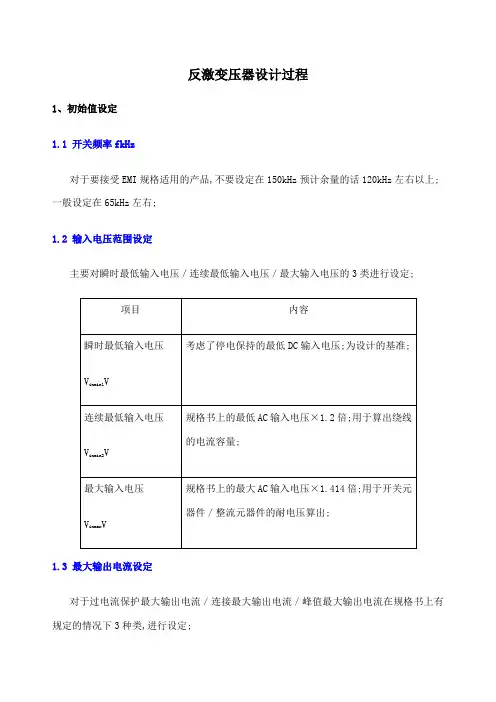
反激变压器设计过程1、初始值设定1.1 开关频率fkHz对于要接受EMI规格适用的产品,不要设定在150kHz预计余量的话120kHz左右以上;一般设定在65kHz左右;1.2 输入电压范围设定主要对瞬时最低输入电压/连续最低输入电压/最大输入电压的3类进行设定;1.3 最大输出电流设定对于过电流保护最大输出电流/连接最大输出电流/峰值最大输出电流在规格书上有规定的情况下3种类,进行设定;另外,在这最大输出电流中需包括对于各自偏差的余量;1.4 最大二次绕组输出端电压设定用以下公式算出:最大二次绕线端输出电压:V N2max V =接插件端输出电压+线间损失0.1~0.5V +整流元器件Vf 0.4~0.6V※ 在有输出电压可变的情况下,根据客户要求规格书的内容不同,适用的范围而各不相同;只保证输出电压 ※只在装置试验时电压可变的情况下; 磁芯用最大输出电压来设计;绕线是用额定输出电压来设计;保证所有的性能※在实际使用条件下通常的电压可变的情况下; 磁芯、绕线都用最大输出电压来设计;1.5 一次电流倾斜率设定输入电压,瞬时最低动作电压、输出电流,在过电流保护最大输出电流/连接最大输出电流/峰值最大输出电流的任意一个最大输出电流的条件下,设定图1-1的一次电流波形的斜率;K 的设定公式如下;作为目标,设定到0.5~0.6,兼顾到之后的其他特性,作最适当的变更;1.6 最大占空比设定一般设定为0.45~0.65;1.7 最大磁通密度设定Bmax设定为磁芯的产品目录上所记载的饱和磁通密度×0.8~0.9;设计的要点:单一输入的情况下设定为0.45、普遍输入的情况下设定为0.65左右;图1-2中表示了TDK 制的磁珠磁芯PC44的B-H 曲线图; 磁芯的磁通密度BT,如图1-2所示,与磁场强度HA/m 成比例,增加;另外,当B 达到一定的值时,在那基础上,即使增加H,B 也不会增加;在此磁束饱和状态下,不仅仅达不到作为变压器的机能,还有开关FET 破损的危险性,因此磁芯绝对必须在此饱和磁通密度以下来使用;另外,从产品目录上引用数据时,需要在符合使用条件的温度下选择饱和磁通密度,因此请注意;※磁芯的饱和磁通密度是根据温度而变动;在TDK 制PC44的120℃下的饱和磁通密度,将降低到25℃时的值的68.6%;因此,如果在25℃的条件下设计的话,有可能发生使用时的故障;1.8 绕线电流密度设定绕线电流密度对绕线的温度上升有一定影响,因此一定要考虑冷却条件、使用温度范围、变压器构造等,再进行适当的设定;设计要点:・ 变压器的发热,是根据,根据磁芯损失的铁损和根据绕线损失的铜损来决定2、变压器特性设计2.1 计算一次绕组的电流峰值变压器总输出功率P 2W 是瞬时最大值;在输出电流规格书中有设定峰值条件的情况下,用I o peak ×V N2max ;另外,多输出的情况下,将各电路的输出功率的总和作为变压器总输出功率;变压器效率一般为0.95;2.2 计算一次/二次绕组的匝数比匝数比根据输出入电压和最大占空比来决定;2.3 计算一次绕组的电感量3、变压器构造设计3.1 计算一次绕组的电流有效值 计算一次绕线电流有效值I N1 TYP RMS ;不用考虑瞬时最低动作输入电压、过电流、峰值最大电流;首先求出占空比α;接着用以上所求出的占空比α,求出一次绕线电流有效值;作为标准,从1.1.8项中设定的绕线电流密度I/SA/mm 2和一次绕线电流有效值I N1typrms A 中,计算出一次绕线截面积S N1mm 2;3.2 计算二次绕组的电流有效值※省略以下的详细计算,可以将直流输入电流的1.6倍作为一※可以省略以下的详细计算,将直流输出电流的1.4倍作为二在实使用条件的通常驻机构状态下,用在1.3.1项中算出的占空比α、一次绕线电流有效值IN1typrmsA,算出连续流出的最大的二次绕线电流有效值;替换为与各自的二次绕线和一次卷的绕线比,进行计算,另※多输出变压器的情况下,将N12中加上对于全功力的其电路输出功力的比率;外在所求得的IN2typrmsA作为标准,从在1.1.8项中设定的绕线电流密度I/SA/mm2与二次绕线电流有效值IN2typrms中,计算出二次绕线断面积Smm2;N2设计要点:・变压器的发热,是根据,根据磁芯损失的铁损和根据绕线损失的铜损来决定的;绕线电流密。

反激变压器的设计————————————————————————————————作者: ————————————————————————————————日期:反激变压器的设计//========================================================反激变压器设计最简单的方法ﻫ我自己综合了一下众多高手的方法,自认为是比较简单的方法了!如下: ﻫ1,VDC min=VAC min * 1.2VDC max=VAC max* 1.42,输出功率Po=P1+P2+Pn......ﻫ上式中P1=(Vo1+Vf)*I1 、P2 =(Vo2+Vf)*I2上式中Vo为输出电压,Vf为整流管压降ﻫ3,输入功率Pin=(Po/η)*1.2(此处1.2为输入整流损耗) ﻫ4,输入平均电流:Iav = Pin/VDCminﻫ5,初级峰值电流:Ip = 2*Iav/Dmax6,初级电感量:Lp=Vdc min *Dmax/(Ip*fs) fs为开关频率ﻫ7,初级匝数:Np=VDC min *Dmax /(ΔB*Ae*fs) ﻫ上式中ΔB推荐取值0.2 Ae为磁芯横截面积,查规格资料可得!8,次级匝数:NS =(Vout+Vd)*(1-Dmax)*Np / Vin min*Dmax至此变压器参数基本完成!另就是线径,可根据具体情况调整!宗旨就是在既定的BOBINN上以合适的线径,绕线平整、饱满!///================================反激式变压器设计原理(FlybackTransformer Design Theory)第一节. 概述.反激式(Flyback)转换器又称单端反激式或"Buck-Boost"转换器.因其输出端在原边绕组断开电源时获得能量故而得名.离线型反激式转换器原理图如图.一、反激式转换器的优点有:2.转换效率高,损失小.1. 电路简单,能高效提供多路直流输出,因此适合多组输出要求.ﻫ4. 输入电压在很大的范围内波动时,仍可有较稳定的输出,目前已可实3. 变压器匝数比值较小. ﻫ现交流输入在85~265V间.无需切换而达到稳定输出的要求.二、反激式转换器的缺点有:1.输出电压中存在较大的纹波,负载调整精度不高,因此输出功率受到限制,通常应用于150W以下.2.转换变压器在电流连续(CCM)模式下工作时,有较大的直流分量,易导致磁芯饱和,所以必须在磁路中加入气隙,从而造成变压器体积变大.3. 变压器有直流电流成份,且同时会工作于CCM/ DCM两种模式,故变压器在设计时较困难,反复调整次数较顺向式多,迭代过程较复杂.ﻫ第二节. 工作原理ﻫ在图1所示隔离反驰式转换器(The isolatedflybackconverter)中, 变压器" T"有隔离与扼流之双重作用.因此" T "又称为Transformer- choke.电路的工作原理如下:ﻫ当开关晶体管Tr ton时,变压器初级Np有电流Ip,并将能量储存于其中(E = LpIp/ 2).由于Np与Ns极性相反,此时二极管D反向偏压而截止,无能量传送到负载.当开关Tr off 时,由楞次定律: (e=-N△Φ/△T)可知,变压器原边绕组将产生一反向电势,此时二极管D正向导通,负载有电流IL流通.反激式转换器之稳态波形如图2.ﻫ由图可知,导通时间ton的大小将决定Ip、Vce的幅值:Vce max = VIN/1-Dmax ﻫVIN:输入直流电压;Dmax: 最大工作周期Dmax = ton/ Tﻫ由此可知,想要得到低的集电极电压,必须保持低的Dmax,也就是Dmax<0.5,在实际应用中通常取Dmax= 0.4,以限制Vcemax≦ 2.2VIN.开关管Tron时的集电极工作电流Ie,也就是原边峰值电流Ip为: Ic = Ip =IL /n.因IL = Io,故当Io一定时,匝比n的大小即决定了Ic的大小,上式是按功率守恒原则,原副边安匝数相等NpIp= NsIs而导出. Ip亦可用下列方法表示:Ic=Ip= 2Po/ (η*VIN*Dmax)η: 转换器的效率公式导出如下:输出功率:Po= LIp2η/ 2T输入电压:VIN = Ldi /dt设di = Ip,且1/ dt = f /Dmax,则:VIN = LIpf/ Dmax或Lp= VIN*Dmax / Ipf则Po又可表示为: ﻫPo= ηVINf DmaxIp2/2f Ip= 1/2ηVINDmaxIp∴Ip=2Po/ηVINDmax上列公式中:ﻫVIN:最小直流输入电压(V)ﻫDmax:最大导通占空比ﻫLp: 变压器初级电感(mH)ﻫIp :变压器原边峰值电流(A)f:转换频率(KHZ)//========================================你看的书就会把你给绕进去...绕半天却找不到自己了。

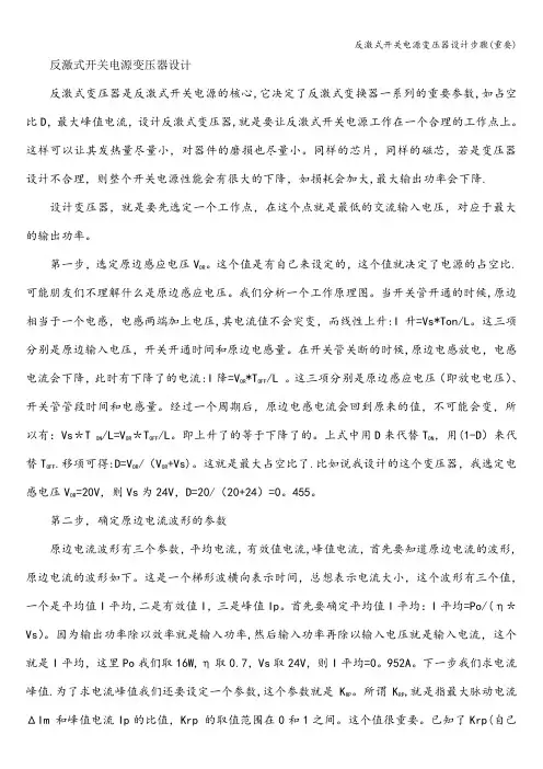
已知条件计算结果输入最低AC 电压:100(V)输出功率:60.00(W)最低电压时工作频率:55(KHz)
损耗功率: 6.67(W)输出电压:40(V)
输入有效电流:0.67(A)输出电流: 1.5(A)
输入峰值电流:0.94(A)输出二极管VF: 1.2(V)
整流二极管VS:141.81(V)占空比:52(%)
MOS 管峰值电流: 3.62(A)MOS 管有效电流: 1.068效率:90(%)
(264V AC 时80V 尖峰)MOS 管V DS:604.36(V)磁通密度:0.25(T)
初级圈数:44.81(TS)修正结果→44(TS)电感量:370(uH)磁芯截面积119(mm²)
次级圈数:12.09(TS)修正结果→12IC 供电电压1:11(V)
供电绕组圈数: 3.50(TS)IC 供电电压2:20(V)
供电绕组圈数: 6.12(TS)当输入AC 电压:220(V)
峰值电流: 2.61(A)此时占空比:33效率:90(%)此时满载工作频率:105.29(KHz)使用小常识将要设计的已知条件填入 红色框内, 绿色框里则得 出计算结果,根据细小的微调,再结合本人的“高频变(TS)压器使用线径及绕线窗口布局工具”即可完美实现。
注意:此工具仅限初学者设计参考,本人不承担任何不良此数值不能大于所用MOS 管耐压值后果。
如有疑问可加 QQ:102 942 3742此设计适用于:SA7527、SY5800/10、iP7302B 、L6562A 等,其他IC 尚未验证,期待您的结果。
(A)(%)设计
基本参
数变压器
部分验证部分单级QR准谐振高频变压器设计工具
红色部分绿色部分。
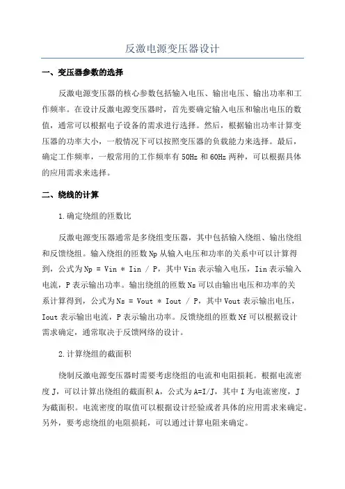
反激电源变压器设计一、变压器参数的选择反激电源变压器的核心参数包括输入电压、输出电压、输出功率和工作频率。
在设计反激电源变压器时,首先要确定输入电压和输出电压的数值,通常可以根据电子设备的需求进行选择。
然后,根据输出功率计算变压器的功率大小,一般情况下可以按照变压器的负载能力来选择。
最后,确定工作频率,一般常用的工作频率有50Hz和60Hz两种,可以根据具体的应用需求来选择。
二、绕线的计算1.确定绕组的匝数比反激电源变压器通常是多绕组变压器,其中包括输入绕组、输出绕组和反馈绕组。
输入绕组的匝数Np从输入电压和功率的关系中可以计算得到,公式为Np = Vin * Iin / P,其中Vin表示输入电压,Iin表示输入电流,P表示输出功率。
输出绕组的匝数Ns可以由输出电压和功率的关系计算得到,公式为Ns = Vout * Iout / P,其中Vout表示输出电压,Iout表示输出电流,P表示输出功率。
反馈绕组的匝数Nf可以根据设计需求确定,通常取决于反馈网络的设计。
2.计算绕组的截面积绕制反激电源变压器时需要考虑绕组的电流和电阻损耗。
根据电流密度J,可以计算出绕组的截面积A,公式为A=I/J,其中I为电流密度,J为截面积。
电流密度的取值可以根据设计经验或者具体的应用需求来确定。
另外,要考虑绕组的电阻损耗,可以通过计算电阻来确定。
3.确定绕组的材料反激电源变压器的绕组通常采用铜导线,因为铜导线有较好的导电性能和热稳定性。
在选择铜导线时,要考虑导线的直径、长度和截面积等参数,同时还要根据绕组的电流来选择合适的导线规格,以保证导线能够承受相应的电流负荷。
三、设计注意事项1.绕制绕组时要注意匝数的计算和绕线的排列方式,以保证绕组的结构紧凑和电感性能的稳定。
2.反激电源变压器中会产生电磁干扰,因此在设计时要合理布局绕组,减小磁感应强度的泄漏。
3.反激电源变压器的绕组要用绝缘材料进行绝缘处理,以避免电气短路和绝缘击穿现象的发生。
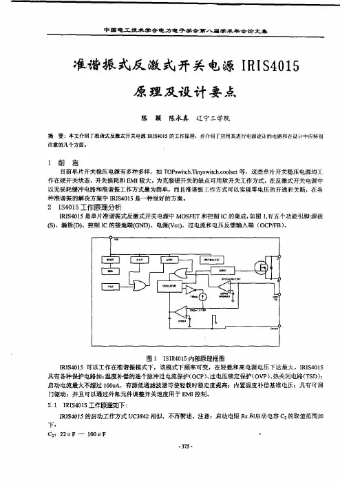
准谐振反激式开关电源设计作者:李惺靳丽钱跃国李向锋来源:《现代电子技术》2013年第21期摘要:设计了一种基于UCC28600控制器的准谐振反激式开关电源电路,分析了准谐振反激式开关电源的工作原理及实现方式,给出了电路及参数设计和选择过程,以及实际工作开关波形。
实验证明,准谐振反激式开关电源具有输入电压范围宽、转换效率高、低EMI、工作稳定可靠的特点。
准谐振技术降低了MOSFET的开关损耗,提高产品可靠性。
此外,更软的开关改善了电源的EMI特性,允许设计人员减少滤波器的数目,降低了产品成本。
关键词:准谐振;反激; CRM; DCM; FFM; UCC28600中图分类号: TN710⁃34 文献标识码: A 文章编号: 1004⁃373X(2013)21⁃0148⁃04准谐振转换是十分成熟的技术,广泛用于消费产品的电源设计中。
新型的绿色电源系列控制器实现低至150 mW的典型超低待机功耗。
本文将阐述准谐振反激式转换器是如何提高电源效率以及如何用UCC28600设计准谐振电源。
1 常规的硬开关反激电路图1所示为常规的硬开关反激式转换器电路。
这种不连续模式反激式转换器(DCM)一个工作周期分为三个工作区间:([t0~][t1])为变压器向负载提供能量阶段,此时输出二极管导通,变压器初级的电流通过Np:Ns的耦合流向输出负载,逐渐减小;MOSFET电压由三部分叠加而成:输入直流电压[VDC、]输出反射电压[VFB、]漏感电压[VLK。
]到[t1]时刻,输出二极管电流减小到0,此时变压器的初级电感和和寄生电容构成一个弱阻尼的谐振电路,周期为2π[LC]。
在停滞区间([t1~][t2]),寄生电容上的电压会随振荡而变化,但始终具有相当大的数值。
当下一个周期[t2]节点,MOSFET 导通时间开始时,寄生电容([COSS]和[CW])上电荷会通过MOSFET放电,产生很大的电流尖峰。
由于这个电流出现时MOSFET存在一个很大的电压,该电流尖峰因此会做成开关损耗。
准谐振反激变换器设计一、拓扑结构选择在准谐振反激变换器设计中,首先需要选择合适的拓扑结构。
常见的反激变换器拓扑包括单端正激、单端反激、双端反激等。
根据实际需求,选择具有所需特性的拓扑结构,如输入输出电压范围、功率等级等。
二、工作原理分析准谐振反激变换器的工作原理是利用磁性元件的储能特性,在开关管导通期间将电能转换为磁能存储在磁芯中,并在开关管截止期间释放磁能转换为电能供给负载。
通过控制开关管的导通与截止时间,实现输入输出电压的转换。
三、输入输出电压范围确定输入输出电压范围是准谐振反激变换器设计的重要步骤。
根据实际应用需求,选择合适的输入输出电压范围。
同时,需要考虑电压调整率和负载调整率等性能指标,以确保变换器的稳定运行。
四、开关频率与磁性元件选择开关频率的选择对准谐振反激变换器的性能具有重要影响。
较高的开关频率可以减小磁性元件的体积,但会增加开关损耗和散热难度。
因此,需要根据实际需求和散热条件,选择合适的开关频率。
同时,需要选择合适的磁性元件,如变压器、电感器等,以满足设计要求。
五、准谐振条件确定准谐振条件是准谐振反激变换器设计的关键参数。
通过调整开关管的导通与截止时间,使开关管在电压或电流达到谐振点附近时进行切换,实现高效的能量传输。
准谐振条件的确定需要考虑磁性元件的参数、输入输出电压和负载条件等因素。
六、驱动与控制电路设计驱动与控制电路是准谐振反激变换器的核心部分。
根据所选的开关管类型和驱动要求,设计合适的驱动电路和控制电路。
驱动电路应提供足够的驱动电流和电压,以满足开关管的驱动需求。
控制电路应实现所需的控制逻辑和保护功能,以确保变换器的稳定运行。
七、热设计与安全工作区考虑热设计是准谐振反激变换器设计中不可忽视的环节。
由于变换器在运行过程中会产生热量,因此需要采取有效的散热措施,如自然散热、强制散热等,以防止过热导致性能下降或损坏。
同时,需要考虑安全工作区,确保变换器在安全条件下工作。
八、电磁兼容性与可靠性评估电磁兼容性是准谐振反激变换器设计中需要考虑的重要因素。
电气传动2024年第54卷第1期ELECTRIC DRIVE 2024Vol.54No.1摘要:设计了一台65W 输出的准谐振反激变换器(QR -Flyback )。
分析了QR -Flyback 的谷底开通原理与开关损耗减小机制,对比了系统在不同工况下的频率特点与损耗特征,总结了变频控制的优势与不足。
结合NCP1380控制器的跳频控制功能,对系统各部分的硬件电路参数进行详细设计,有效提升了整机效率。
最后,通过仿真和实验验证了理论分析与参数设计的可行性。
关键词:准谐振反激变换器;谷底开通;跳频控制中图分类号:TM923文献标识码:ADOI :10.19457/j.1001-2095.dqcd24545Analysis and Design of Quasi -resonant Flyback Converter WU Qing ,AN Shaoliang ,XU Yixuan ,DONG Songsong(School of Electrical Engineering ,Xi'an University of Technology ,Xi ’an 710000,Shaanxi ,China )Abstract:A quasi-resonant Flyback (QR-Flyback )converter with 65W output was designed.The valley switching principle and the switching loss reduction mechanism of QR-Flyback were analyzed ,the frequency and loss characteristics of the system under different working conditions were compared ,and the advantages and disadvantages of frequency conversion control were bined with the frequency hopping control function of the NCP1380controller ,the hardware circuit parameters of each part of the system were designed and the efficiency of the system was effectively improved.Finally ,the feasibility of theoretical analysis and parameter design were verified by simulation and experiment.Key words:quasi-resonant Flyback (QR-Flyback );valley switching ;frequency hopping control作者简介:吴庆(1999—),女,硕士研究生,Email :*****************准谐振Flyback 变换器分析与设计吴庆,安少亮,徐义轩,董松松(西安理工大学电气工程学院,陕西西安710000)随着移动互联网的普及,各种电子设备层出不穷,其供电电源的需求也在不断上升,而反激变换器(Flyback )因其结构简单且可提供电气隔离的特点,在此类小功率场合获得了广泛应用。
1〕反激式变压器设计介绍反激式电源变换器设计的关键因素之一是变压器的设计。
在此我们所说的变压器不是真正意义上的变压器,而更多的是一个能量存储装置。
在变压器初级导通期间能量存储在磁芯的气隙中,关断期间存储的能量被传送给输出。
初次级的电流不是同时流动的。
因此它更多的被认为是一个带有次级绕组的电感。
反激电路的主要优势是成本,简单和容易得到多路输出。
反激式拓扑对于100W 以内的系统是实用和廉价的。
大于100W的系统由于着重降低装置的电压和电流,其它诸如正激变换器方式就变得更有成效。
反激式变压器设计是一个反复的过程,因为与它的变量个数有关,但是它不是很困难,稍有经验就可快速和容易的处理。
在变压器设计之前的重点是定义电源参数,诸如输入电压,输出功率,最小工作频率,最大占空比等。
根据这些我们就可以计算出变压器参数,选择合适的磁芯。
如果计算参数没有落在设计范围内,重复计算是必要的。
利用网站上的EXCEL电子表格可以容易的处理这些步骤。
属于ISMPS IC的IR40xx系列最初设计应用于准谐振方式,这意味变压器工作于不连续模式(磁场不连续,当变压器中的能量传递到次边后磁场反回到零)。
在PRC模式中的变压器通常也工作于不连续状态,若工作于连续状态时工作频率设置的很低(约20KHZ时一般不实用,因为需要较大尺寸的磁芯)。
因此本应用手册仅包含不连续设计的实例。
2〕电源设计所需的标准在开始变压器设计之前,根据电源的规范必须定义一些参数如下:1〕最小工作频率-fmin2〕预计电源效率-η≈0.85~0.9(高压输出),0.75~0.85(低压输出)3〕最小直流总线电压-Vmin如110V时最小输入电压85Vac,可有10V抖动) 4〕最大占空比-Dm(建议最大值为0.5)5)串联谐振电容值-Cres〔建议取值范围为100pf~1.5nf,见图1〕3〕变压器设计步骤首先计算总输出功率,它包括所有次级输出功率,辅助输出功率和输出二极管的压降。