最新C++032循环控制结构
- 格式:ppt
- 大小:681.50 KB
- 文档页数:7
水温控制系统目录摘要 (2)1. 方案论证 (3)1.1 题目解析 (3)1.2 各种方案比较与选择 (3)2. 系统硬件设计 (4)2.1 系统的总体设计 (4)2.2 单元电路设计 (4)2.21温度采集模块 (4)2.22单片机控制模块 (5)2.23键盘输入 (5)2.24液晶显示模块 (5)2.25控制模块 (6)2.3 发挥部分设计与实现 (6)2.31报警模块 (7)3. 系统软件设计 (8)3.1程序总体设计 (8)4. 测试结果及其分析 (8)总结 (9)附录一 (10)附录二 (10)摘要:此温度自动控制系统可以实现手动设定的标准温度和实测温度进行比较以实现自动控制温度的调节。
该系统利用STC89C52单片机作为主控芯片,采用数字式温度传感器DS18B20测量所需的温度,温度误差可达±0.5℃。
图形、数据显示使用12864字符液晶,可以形象的显示测得的温度以及温度的变化曲线。
此系统包括温度采集模块、键盘输入模块、单片机主控模块、报警模块、液晶显示模块、控制模块、加热器、制冷器。
本系统通过并行通信实现温度设定、控制和显示,有体积小、交互性强等优点。
为了实现高精度的水温控制,本单片机系统采用PID算法控制技术,通过控制加热棒、半导体制冷片和电源的接通、断开,从而改变水温加热或制冷时间的方法来实现对水温的控制。
关键词:STC89C52 DS18B20 加热制冷温度自动控制1. 方案论证1.1 题目解析根据命题要求设计制作一个水温自动控制系统,水温可以在10℃—70℃量程范围内实现人工设定,并且在环境温度降低或升高时实现自动控制,。
主要性能指标有:(1)可键盘设定控制温度值,并能用液晶显示,显示最小区分度为0.1℃;(2)可以测量并显示水的实际温度。
温度测量误差在±0.5℃内;(3)水温控制系统应具有全量程(10℃—70℃)内的升温、降温功能(降温可用半导体制冷片、升温用800W以内的电加热器);(4)在全量程内任意设定一个温度值(例如起始温度±15℃内),控制系统可以实现该给定温度的恒值自动控制。

C32位实时控制器C2000 32 位实时控制器软件概念 | DMC 系统 | 系统注意事项 | 器件功能自 1996 年推出 TMS320F24x 系列以来,C2000 实时控制器平台一直是数字电机控制领域的业界领先者。
2002 年,TI 首次推出基于 C28x DSP 引擎的F281x 系列,成为专门针对高性能、数学密集电源电子产品控制而打造的首个32 位架构。
在 C28x 的基础上,我们创建了一系列代码兼容器件,以满足应用程序在性能、价格、外引脚及外设方面的各种需求。
C2000 MCU 用于各种三相电机应用,包括 AC 伺服驱动、精密运动控制、电子动力转向、HVAC 压缩器和鼓风机、工业泵以及洗衣机和电冰箱压缩器等设备。
借助 C2000 的如下功能,使用 C2000 的客户均已大获成功:•对无传感器操作和场定向控制 (FOC) 进行精确计算的一流功能•基础软件例程的电机控制库,以及随附的理论、文档和系统示例•高速、高精度片上模数转换器以及对速度或精度甚至更高的外部 ADC 的轻松支持•功能丰富的 PWM 发生器和支持任何系统电源拓扑的故障检测•合作伙伴提供的图形模拟、系统开发和自动代码生成工具C2000 电机控制软件概念•最高精度和最高数字准确度•实现最简单重用和定制的模块化库(C 源码)•消除定点调节和饱和压力•最容易针对您的自定义电机进行调优•文档:理论、软件、系统、BOM、原理图放大•电机控制基础软件块库(提供源码)o转换器和评估器:Clarke、Parke、滑动模式查看器、相压计算器、通量和速度计算器及评估器、解析器计算器o控制:信号生成、PID、BEMF 换向、空间矢量发生器o外设驱动器:适用于不同的模式和拓扑 - ADC、PWM、编码器、传感器捕获•具有可变输入和可变输出的模块化结构或宏•初始化时定义所有变量并将一个块的输出设置为下一个块的输入•运行时调用结构或宏函数•每个模块均提供完整文档 - 包括数学和 DMC 理论DMC 系统:以增量方式连接块放大通过使用 DMC 库模块,我们逐步建立了完整的电机控制系统示例。


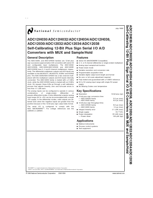
ADC12H030/ADC12H032/ADC12H034/ADC12H038,ADC12030/ADC12032/ADC12034/ADC12038Self-Calibrating 12-Bit Plus Sign Serial I/O A/D Converters with MUX and Sample/HoldGeneral DescriptionThe ADC12030,and ADC12H030families are 12-bit plus sign successive approximation A/D converters with serial I/O and configurable input multiplexers.The ADC12032/ADC12H032,ADC12034/ADC12H034and ADC12038/ADC12H038have 2,4and 8channel multiplexers,respec-tively.The differential multiplexer outputs and A/D inputs are available on the MUXOUT1,MUXOUT2,A/DIN1and A/DIN2pins.The ADC12030/ADC12H030has a two channel multi-plexer with the multiplexer outputs and A/D inputs internally connected.The ADC12030family is tested with a 5MHz clock,while the ADC12H030family is tested with an 8MHz clock.On request,these A/Ds go through a self calibration process that adjusts linearity,zero and full-scale errors to less than ±1LSB each.The analog inputs can be configured to operate in various combinations of single-ended,differential,or pseudo-differential modes.A fully differential unipolar analog input range (0V to +5V)can be accommodated with a single +5V supply.In the differential modes,valid outputs are ob-tained even when the negative inputs are greater than the positive because of the 12-bit plus sign output data format.The serial I/O is configured to comply with the NSC MICROWIRE ™.For voltage references see the LM4040or LM4041.Featuresn Serial I/O (MICROWIRE Compatible)n 2,4,or 8channel differential or single-ended multiplexer n Analog input sample/hold function n Power down moden Variable resolution and conversion rate n Programmable acquisition timen Variable digital output word length and format n No zero or full scale adjustment requiredn Fully tested and guaranteed with a 4.096V reference n0V to 5V analog input range with single 5V power supplyn No Missing Codes over temperatureKey Specificationsn Resolution12-bit plus sign n 12-bit plus sign conversion time —ADC12H030family 5.5µs (max)—ADC12030family8.8µs (max)n 12-bit plus sign throughput time —ADC12H030family 8.6µs (max)—ADC12030family 14µs (max)n Integral linearity error ±1LSB (max)n Single supply 5V ±10%n Power dissipation 33mW (max)—Power down100µW (typ)Applicationsn Medical instrumentsn Process control systems n Test equipmentTRI-STATE ®is a registered trademark of National Semiconductor Corporation.COPS ™microcontrollers,HPC ™and MICROWIRE ™are trademarks of National Semiconductor Corporation.July 1999ADC12H030/ADC12H032/ADC12H034/ADC12H038,ADC12030/ADC12032/ADC12034/ADC12038Self-Calibrating 12-Bit Plus Sign Serial I/O A/D Converters with MUX and Sample/Hold©1999National Semiconductor Corporation ADC12038Simplified Block DiagramConnection DiagramsDS011354-116-Pin Wide Body SO PackagesDS011354-6Top View20-Pin Wide Body SO PackagesDS011354-7Top View 2Connection Diagrams(Continued)Ordering InformationIndustrial Temperature Range Package−40˚C≤T A≤+85˚CADC12H030CIWM,ADC12030CIWM M16BADC12H032CIWM,ADC12032CIWM M20BADC12H034CIN,ADC12034CIN N24CADC12H034CIWM,ADC12034CIWM M24BADC12H038CIWM,ADC12038CIWM M28B Pin DescriptionsCCLK The clock applied to this input controls thesucessive approximation conversion timeinterval and the acquisition time.The riseand fall times of the clock edges should notexceed1µs.SCLK This is the serial data clock input.The clockapplied to this input controls the rate atwhich the serial data exchange occurs.Therising edge loads the information on the DIpin into the multiplexer address and modeselect shift register.This address controlswhich channel of the analog input multi-plexer(MUX)is selected and the mode ofoperation for the A/D.With CS low the fall-ing edge of SCLK shifts the data resultingfrom the previous ADC conversion out onDO,with the exception of the first bit of data.When CS is low continously,the first bit ofthe data is clocked out on the rising edge ofEOC(end of conversion).When CS istoggled the falling edge of CS always clocksout the first bit of data.CS should bebrought low when SCLK is low.The rise andfall times of the clock edges should not ex-ceed1µs.DI This is the serial data input pin.The data ap-plied to this pin is shifted by the rising edgeof SCLK into the multiplexer address andmode select register.Table2through Table5show the assignment of the multiplexeraddress and the mode select data.DO The data output pin.This pin is an activepush/pull output when CS is low.When CSis high,this output is TRI-STATE.The A/Dconversion result(D0–D12)and converterstatus data are clocked out by the fallingedge of SCLK on this pin.The word lengthand format of this result can vary(see Table1).The word length and format are con-trolled by the data shifted into the multi-plexer address and mode select register(see Table5).EOC This pin is an active push/pull output and in-dicates the status of the ADC12030/2/4/8.When low,it signals that the A/D is busy witha conversion,auto-calibration,auto-zero orpower down cycle.The rising edge of EOCsignals the end of one of these cycles.CS This is the chip select pin.When a logic lowis applied to this pin,the rising edge ofSCLK shifts the data on DI into the addressregister.This low also brings DO out ofTRI-STATE.With CS low the falling edge ofSCLK shifts the data resulting from the pre-vious ADC conversion out on DO,with the24-Pin Wide BodySO PackagesDS011354-8 Top View28-Pin Wide BodySO Packages 3Pin Descriptions(Continued)exception of the first bit of data.When CS islow continously,the first bit of the data isclocked out on the rising edge of EOC(endof conversion).When CS is toggled the fall-ing edge of CS always clocks out the first bitof data.CS should be brought low whenSCLK is low.The falling edge of CS resets aconversion in progress and starts the se-quence for a new conversion.When CS isbrought back low during a conversion,thatconversion is prematurely terminated.Thedata in the output latches may be corrupted.Therefore,when CS is brought back lowduring a conversion in progress the dataoutput at that time should be ignored.CSmay also be left continuously low.In thiscase it is imperative that the correct numberof SCLK pulses be applied to the ADC in or-der to remain synchronous.After the ADCsupply power is applied it expects to see13clock pulses for each I/O sequence.Thenumber of clock pulses the ADC expects isthe same as the digital output word length.This word length can be modified by thedata shifted in on the DO pin.Table5detailsthe data required.DOR This is the data output ready pin.This pin isan active push/pull output.It is low when theconversion result is being shifted out andgoes high to signal that all the data hasbeen shifted out.CONV A logic low is required on this pin to programany mode or change the ADC’s configura-tion as listed in the Mode ProgrammingTable5such as12-bit conversion,8-bit con-version,Auto Cal,Auto Zero etc.When thispin is high the ADC is placed in the readdata only mode.While in the read data onlymode,bringing CS low and pulsing SCLKwill only clock out on DO any data stored inthe ADCs output shift register.The data onDI will be neglected.A new conversion willnot be started and the ADC will remain inthe mode and/or configuration previouslyprogrammed.Read data only cannot beperformed while a conversion,Auto-Cal orAuto-Zero are in progress.PD This is the power down pin.When PD ishigh the A/D is powered down;when PD islow the A/D is powered up.The A/D takes amaximum of250µs to power up after thecommand is given.CH0–CH7These are the analog inputs of the MUX.Achannel input is selected by the address in-formation at the DI pin,which is loaded onthe rising edge of SCLK into the addressregister(See Tables2,3,4).The voltage applied to these inputs shouldnot exceed V A+or go below GND.Exceed-ing this range on an unselected channel willcorrupt the reading of a selected channel. COM This pin is another analog input pin.It isused as a pseudo ground when the analogmultiplexer is single-ended.MUXOUT1,MUXOUT2These are the multiplexer outputpins.A/DIN1,/DIN2These are the converter input pins.MUX-OUT1is usually tied to A/DIN1.MUXOUT2is usually tied to A/DIN2.If external circuitryis placed between MUXOUT1and A/DIN1,or MUXOUT2and A/DIN2it may be neces-sary to protect these pins.The voltage atthese pins should not exceed V A+or go be-low AGND(see Figure5).V REF+This is the positive analog voltage referenceinput.In order to maintain accuracy,thevoltage range of V REF(V REF=V REF+−V REF−)is1V DC to5.0V DC and the voltageat V REF+cannot exceed V A+.See Figure6for recommended bypassing.V REF−The negative voltage reference input.In or-der to maintain accuracy,the voltage at thispin must not go below GND or exceed V A+.(See Figure6).V A+,V D+These are the analog and digital power sup-ply pins.V A+and V D+are not connected to-gether on the chip.These pins should betied to the same power supply and by-passed separately(see Figure6).The oper-ating voltage range of V A+and V D+is4.5V DC to5.5V DC.DGND This is the digital ground pin(see Figure6). AGND This is the analog ground pin(see Figure6).4Absolute Maximum Ratings (Notes 1,2)If Military/Aerospace specified devices are required,please contact the National Semiconductor Sales Office/Distributors for availability and specifications.Positive Supply Voltage (V +=V A +=V D +)6.5VVoltage at Inputs and Outputs except CH0–CH7and COM −0.3V to V ++0.3V Voltage at Analog Inputs CH0–CH7and COM GND −5V to V ++5V|V A +−V D +|300mV Input Current at Any Pin (Note 3)±30mA Package Input Current (Note 3)±120mAPackage Dissipation at T A =25˚C (Note 4)500mW ESD Susceptability (Note 5)Human Body Model 1500V Soldering InformationN Packages (10seconds)260˚CSO Package (Note 6):Vapor Phase (60seconds)215˚C Infrared (15seconds)220˚CStorage Temperature−65˚C to +150˚COperating Ratings (Notes 1,2)Operating Temperature Range T MIN ≤T A ≤T MAXADC12030CIWM,ADC12H030CIWM,ADC12032CIWM,ADC12H032CIWM,ADC12034CIN,ADC12034CIWM,ADC12H034CIN,ADC12H034CIWM,ADC12038CIWM,ADC12H038CIWM−40˚C ≤T A ≤+85˚CSupply Voltage (V +=V A +=V D +)+4.5V to +5.5V|V A +−V D +|≤100mV V REF +0V to V A +V REF −0V to V REF +V REF (V REF +−V REF −)1V to V A +V REF Common Mode Voltage Range0.1V A +to 0.6V A +A/DIN1,A/DIN2,MUXOUT1and MUXOUT2Voltage Range 0V to V A +A/D IN Common Mode Voltage Range0V to V A +Converter Electrical CharacteristicsThe following specifications apply for V +=V A +=V D +=+5.0V DC ,V REF +=+4.096V DC ,V REF −=0V DC ,12-bit +sign conver-sion mode,f CK =f SK =8MHz for the ADC12H030,ADC12H032,ADC12H034and ADC12H038,f CK =f SK =5MHz for the ADC12030,ADC12032,ADC12034and ADC12038,R S =25Ω,source impedance for V REF +and V REF −≤25Ω,fully-differential input with fixed 2.048V common-mode voltage,and 10(t CK )acquisition time unless otherwise specified.Boldface limits apply for T A =T J =T MIN to T MAX ;all other limits T A =T J =25˚C.(Notes 7,8,9)SymbolParameterConditionsTypical (Note 10)Limits (Note 11)Units (Limits)STATIC CONVERTER CHARACTERISTICSResolution with No Missing Codes12+signBits (min)+ILE Positive Integral Linearity Error After Auto-Cal (Notes 12,18)±1/2±1LSB (max)−ILE Negative Integral Linearity Error After Auto-Cal (Notes 12,18)±1/2±1LSB (max)DNLDifferential Non-Linearity After Auto-Cal±1LSB (max)Positive Full-Scale Error After Auto-Cal (Notes 12,18)±1/2±3.0LSB (max)Negative Full-Scale Error After Auto-Cal (Notes 12,18)±1/2±3.0LSB (max)Offset ErrorAfter Auto-Cal (Notes 5,18)±1/2±2LSB (max)V IN (+)=V IN (−)=2.048V DC Common Mode ErrorAfter Auto-Cal (Note 15)±2±3.5LSB (max)TUETotal Unadjusted ErrorAfter Auto-Cal ±1LSB(Notes 12,13,14)Resolution with No Missing Codes8-bit +sign mode8+signBits (min)+INL Positive Integral Linearity Error 8-bit +sign mode (Note 12)±1/2LSB (max)−INL Negative Integral Linearity Error 8-bit +sign mode (Note 12)±1/2LSB (max)DNLDifferential Non-Linearity 8-bit +sign mode±3/4LSB (max)Positive Full-Scale Error 8-bit +sign mode (Note 12)±1/2LSB (max)Negative Full-Scale Error8-bit +sign mode (Note 12)±1/2LSB (max)5Converter Electrical Characteristics(Continued)The following specifications apply for V+=V A+=V D+=+5.0V DC,V REF+=+4.096V DC,V REF−=0V DC,12-bit+sign conver-sion mode,f CK=f SK=8MHz for the ADC12H030,ADC12H032,ADC12H034and ADC12H038,f CK=f SK=5MHz for the ADC12030,ADC12032,ADC12034and ADC12038,R S=25Ω,source impedance for V REF+and V REF−≤25Ω,fully-differential input with fixed2.048V common-mode voltage,and10(t CK)acquisition time unless otherwise specified.Boldface limits apply for T A=T J=T MIN to T MAX;all other limits T A=T J=25˚C.(Notes7,8,9)Symbol Parameter Conditions Typical(Note10)Limits(Note11)Units(Limits)STATIC CONVERTER CHARACTERISTICSOffset Error8-bit+sign mode,after Auto-Zero(Note13)±1/2LSB(max)V IN(+)=V IN(−)=+2.048VTUE Total Unadjusted Error8-bit+sign modeafter Auto-Zero±3/4LSB(max)(Notes12,13,14)Multiplexer Channelto Channel Matching±0.05LSB Power Supply Sensitivity V+=+5V±10%V REF=+4.096VOffset Error±0.5±1LSB(max) +Full-Scale Error±0.5±1.5LSB(max)−Full-Scale Error±0.5±1.5LSB(max) +Integral Linearity Error±0.5LSB−Integral Linearity Error±0.5LSB Output Data from(Note20)+10LSB(max)“12-Bit Conversion of Offset”−10LSB(min) (see Table5)Output Data from(Note20)4095LSB(max)“12-Bit Conversion of Full-Scale”4093LSB(min) (see Table5)UNIPOLAR DYNAMIC CONVERTER CHARACTERISTICSS/(N+D)Signal-to-Noise Plus f IN=1kHz,V IN=5V PP,V REF+=5.0V69.4dB Distortion Ratio f IN=20kHz,V IN=5V PP,V REF+=5.0V68.3dBf IN=40kHz,V IN=5V PP,V REF+=5.0V65.7dB−3dB Full Power Bandwidth V IN=5V PP,where S/(N+D)drops3dB31kHz DIFFERENTIAL DYNAMIC CONVERTER CHARACTERISTICSS/(N+D)Signal-to-Noise Plus f IN=1kHz,V IN=±5V,V REF+=5.0V77.0dB Distortion Ratio f IN=20kHz,V IN=±5V,V REF+=5.0V73.9dBf IN=40kHz,V IN=±5V,V REF+=5.0V67.0dB−3dB Full Power Bandwidth V IN=±5V,where S/(N+D)drops3dB40kHz REFERENCE INPUT,ANALOG INPUTS AND MULTIPLEXER CHARACTERISTICSC REF Reference Input Capacitance85pFC A/D A/DIN1and A/DIN2Analog75pFInput CapacitanceA/DIN1and A/DIN2Analog V IN=+5.0V or±0.1±1.0µA(max)Input Leakage Current V IN=0VCH0–CH7and COM GND−0.05V(min)Input Voltage V A++0.05V(max) C CH CH0–CH7and COMInput Capacitance10pFC MUXOUT MUX Output Capacitance20pF 6Converter Electrical Characteristics(Continued)The following specifications apply for V+=V A+=V D+=+5.0V DC,V REF+=+4.096V DC,V REF−=0V DC,12-bit+sign conver-sion mode,f CK=f SK=8MHz for the ADC12H030,ADC12H032,ADC12H034and ADC12H038,f CK=f SK=5MHz for the ADC12030,ADC12032,ADC12034and ADC12038,R S=25Ω,source impedance for V REF+and V REF−≤25Ω,fully-differential input with fixed2.048V common-mode voltage,and10(t CK)acquisition time unless otherwise specified.Boldface limits apply for T A=T J=T MIN to T MAX;all other limits T A=T J=25˚C.(Notes7,8,9)Symbol Parameter Conditions Typical(Note10)Limits(Note11)Units(Limits)REFERENCE INPUT,ANALOG INPUTS AND MULTIPLEXER CHARACTERISTICSOff Channel Leakage(Note16)On Channel=5V and−0.01−0.3µA(min)CH0–CH7and COM Pins Off Channel=0VOn Channel=0V and0.010.3µA(max)Off Channel=5VOn Channel Leakage(Note16)On Channel=5V and0.010.3µA(max)CH0–CH7and COM Pins Off Channel=0VOn Channel=0V and−0.01−0.3µA(min)Off Channel=5VMUXOUT1and MUXOUT2V MUXOUT=5.0V or0.010.3µA(max)Leakage Current V MUXOUT=0VR ON MUX On Resistance V IN=2.5V and8501150Ω(max)V MUXOUT=2.4VR ON Matching Channel V IN=2.5V and5%to Channel V MUXOUT=2.4VChannel to Channel Crosstalk V IN=5V PP,f IN=40kHz−72dBMUX Bandwidth90kHz DC and Logic Electrical CharacteristicsThe following specifications apply for V+=V A+=V D+=+5.0V DC,V REF+=+4.096V DC,V REF−=0V DC,12-bit+sign conver-sion mode,f CK=f SK=8MHz for the ADC12H030,ADC12H032,ADC12H034and ADC12H038,f CK=f SK=5MHz for theADC12030,ADC12032,ADC12034and ADC12038,R S=25Ω,source impedance for V REF+and V REF−≤25Ω,fully-differential input with fixed2.048V common-mode voltage,and10(t CK)acquisition time unless otherwise specified.Boldface limits applyfor T A=T J=T MIN to T MAX;all other limits T A=T J=25˚C.(Notes7,8,9)Symbol Parameter Conditions Typical Limits Units(Note10)(Note11)(Limits) CCLK,CS,CONV,DI,PD AND SCLK INPUT CHARACTERISTICSV IN(1)Logical“1”Input Voltage V+=5.5V 2.0V(min)V IN(0)Logical“0”Input Voltage V+=4.5V0.8V(max)I IN(1)Logical“1”Input Current V IN=5.0V0.005 1.0µA(max)I IN(0)Logical“0”Input Current V IN=0V−0.005−1.0µA(min) DO,EOC AND DOR DIGITAL OUTPUT CHARACTERISTICSV OUT(1)Logical“1”Output Voltage V+=4.5V,I OUT=−360µA 2.4V(min)V+=4.5V,I OUT=−10µA 4.25V(min)V OUT(0)Logical“0”Output Voltage V+=4.5V,I OUT=1.6mA0.4V(max)I OUT TRI-STATE®Output Current V OUT=0V−0.1−3.0µA(max)V OUT=5V0.1 3.0µA(max)+I SC Output Short Circuit Source Current V OUT=0V14 6.5mA(min)−I SC Output Short Circuit Sink Current V OUT=V D+168.0mA(min) POWER SUPPLY CHARACTERISTICSI D+Digital Supply Current Awake 1.6 2.5mA(max)ADC12030,ADC12032,ADC12034CS=HIGH,Powered Down,CCLK on600µAand ADC12038CS=HIGH,Powered Down,CCLK off20µADigital Supply Current Awake 2.3 3.2mAADC12H030,ADC12H032,CS=HIGH,Powered Down,CCLK on0.9mAADC12H034and ADC12H038CS=HIGH,Powered Down,CCLK off20µA7DC and Logic Electrical Characteristics(Continued)The following specifications apply for V+=V A+=V D+=+5.0V DC,V REF+=+4.096V DC,V REF−=0V DC,12-bit+sign conver-sion mode,f CK=f SK=8MHz for the ADC12H030,ADC12H032,ADC12H034and ADC12H038,f CK=f SK=5MHz for the ADC12030,ADC12032,ADC12034and ADC12038,R S=25Ω,source impedance for V REF+and V REF−≤25Ω,fully-differential input with fixed2.048V common-mode voltage,and10(t CK)acquisition time unless otherwise specified.Boldface limits apply for T A=T J=T MIN to T MAX;all other limits T A=T J=25˚C.(Notes7,8,9)Symbol Parameter Conditions Typical Limits Units(Note10)(Note11)(Limits) POWER SUPPLY CHARACTERISTICSI A+Positive Analog Supply Current Awake 2.7 4.0mA(max)CS=HIGH,Powered Down,CCLK on10µACS=HIGH,Powered Down,CCLK off0.1µAI REF Reference Input Current Awake70µACS=HIGH,Powered Down0.1µA AC Electrical CharacteristicsThe following specifications apply for V+=V A+=V D+=+5.0V DC,V REF+=+4.096V DC,V REF−=0V DC,12-bit+sign conver-sion mode,t r=t f=3ns,f CK=f SK=8MHz for the ADC12H030,ADC12H032,ADC12H034and ADC12H038,f CK=f SK=5 MHz for the ADC12030,ADC12032,ADC12034and ADC12038,R S=25Ω,source impedance for V REF+and V REF−≤25Ω, fully-differential input with fixed2.048V common-mode voltage,and10(t CK)acquisition time unless otherwise specified.Bold-face limits apply for T A=T J=T MIN to T MAX;all other limits T A=T J=25˚C.(Note17)Symbol Parameter Conditions Typical(Note10)ADC12H030/2/4/8ADC12030/2/4/8Units(Limits) Limits Limits(Note11)(Note11)f CK Conversion Clock1085MHz(max)(CCLK)Frequency1MHz(min) f SK Serial Data Clock1085MHz(max)SCLK Frequency0Hz(min)Conversion Clock4040%(min)Duty Cycle6060%(max)Serial Data Clock4040%(min)Duty Cycle6060%(max) t C Conversion Time12-Bit+Sign or12-Bit44(t CK)44(t CK)44(t CK)(max)5.58.8µs(max)8-Bit+Sign or8-Bit21(t CK)21(t CK)21(t CK)(max)2.625 4.2µs(max) t A Acquisition Time6Cycles Programmed6(t CK)6(t CK)6(t CK)(min) (Note19)7(t CK)7(t CK)(max)0.75 1.2µs(min)0.875 1.4µs(max)10Cycles Programmed10(t CK)10(t CK)10(t CK)(min)11(t CK)11(t CK)(max)1.252.0µs(min)1.3752.2µs(max)18Cycles Programmed18(t CK)18(t CK)18(t CK)(min)19(t CK)19(t CK)(max)2.253.6µs(min)2.3753.8µs(max)34Cycles Programmed34(t CK)34(t CK)34(t CK)(min)35(t CK)35(t CK)(max)4.25 6.8µs(min)4.3757.0µs(max) 8AC Electrical Characteristics(Continued)The following specifications apply for V+=V A+=V D+=+5.0V DC,V REF+=+4.096V DC,V REF−=0V DC,12-bit+sign conver-sion mode,t r=t f=3ns,f CK=f SK=8MHz for the ADC12H030,ADC12H032,ADC12H034and ADC12H038,f CK=f SK=5 MHz for the ADC12030,ADC12032,ADC12034and ADC12038,R S=25Ω,source impedance for V REF+and V REF−≤25Ω, fully-differential input with fixed2.048V common-mode voltage,and10(t CK)acquisition time unless otherwise specified.Bold-face limits apply for T A=T J=T MIN to T MAX;all other limits T A=T J=25˚C.(Note17)Symbol Parameter Conditions Typical(Note10)ADC12H030/2/4/8ADC12030/2/4/8Units(Limits) Limits Limits(Note11)(Note11)t CKAL Self-Calibration Time4944(t CK)4944(t CK)4944(t CK)(max)618.0988.8µs(max) t AZ Auto-Zero Time76(t CK)76(t CK)76(t CK)(max)9.515.2µs(max) t SYNC Self-Calibration2(t CK)2(t CK)2(t CK)(min) or Auto-Zero3(t CK)3(t CK)(max)Synchronization Time0.2500.40µs(min) from DOR0.3750.60µs(max) t DOR DOR High Time9(t SK)9(t SK)9(t SK)(max) when CS is Low 1.125 1.8µs(max) Continuously for ReadData and SoftwarePower Up/Downt CONV CONV Valid Data Time8(t SK)8(t SK)8(t SK)(max)1.0 1.6µs(max) AC Electrical CharacteristicsThe following specifications apply for V+=V A+=V D+=+5.0V DC,V REF+=+4.096V DC,V REF−=0V DC,12-bit+sign conver-sion mode,t r=t f=3ns,f CK=f SK=8MHz for the ADC12H030,ADC12H032,ADC12H034and ADC12H038,f CK=f SK=5 MHz for the ADC12030,ADC12032,ADC12034and ADC12038,R S=25Ω,source impedance for V REF+and V REF−≤25Ω, fully-differential input with fixed2.048V common-mode voltage,and10(t CK)acquisition time unless otherwise specified.Bold-face limits apply for T A=T J=T MIN to T MAX;all other limits T A=T J=25˚C.(Note17)Symbol Parameter Conditions Typical(Note10)Limits(Note11)Units(Limits)t HPU Hardware Power-Up Time,Time from140250µs(max) PD Falling Edge to EOC Rising Edget SPU Software Power-Up Time,Time fromSerial Data Clock Falling Edge to140250µs(max)EOC Rising Edget ACC Access Time Delay from2050ns(max) CS Falling Edge to DO Data Validt SET-UP Set-Up Time of CS Falling Edge to30ns(min) Serial Data Clock Rising Edget DELAY Delay from SCLK Falling05ns(min) Edge to CS Falling Edget1H,t0H Delay from CS Rising Edge to R L=3k,C L=100pF40100ns(max) DO TRI-STATEt HDI DI Hold Time from Serial Data515ns(min) Clock Rising Edget SDI DI Set-Up Time from Serial Data510ns(min) Clock Rising Edget HDO DO Hold Time from Serial Data R L=3k,C L=100pF2550ns(max) Clock Falling Edge5ns(min)t DDO Delay from Serial Data Clock3550ns(max) Falling Edge to DO Data Valid9AC Electrical Characteristics(Continued)The following specifications apply for V+=V A+=V D+=+5.0V DC,V REF+=+4.096V DC,V REF−=0V DC,12-bit+sign conver-sion mode,t r=t f=3ns,f CK=f SK=8MHz for the ADC12H030,ADC12H032,ADC12H034and ADC12H038,f CK=f SK=5 MHz for the ADC12030,ADC12032,ADC12034and ADC12038,R S=25Ω,source impedance for V REF+and V REF−≤25Ω, fully-differential input with fixed2.048V common-mode voltage,and10(t CK)acquisition time unless otherwise specified.Bold-face limits apply for T A=T J=T MIN to T MAX;all other limits T A=T J=25˚C.(Note17)Symbol Parameter Conditions Typical(Note10)Limits(Note11)Units(Limits)t RDO DO Rise Time,TRI-STATE to High R L=3k,C L=100pF1030ns(max) DO Rise Time,Low to High1030ns(max) t FDO DO Fall Time,TRI-STATE to Low R L=3k,C L=100pF1230ns(max) DO Fall Time,High to Low1230ns(max) t CD Delay from CS Falling Edge2545ns(max) to DOR Falling Edget SD Delay from Serial Data Clock Falling2545ns(max) Edge to DOR Rising EdgeC IN Capacitance of Logic Inputs10pFC OUT Capacitance of Logic Outputs20pFNote1:Absolute Maximum Ratings indicate limits beyond which damage to the device may occur.Operating Ratings indicate conditions for which the device is func-tional,but do not guarantee specific performance limits.For guaranteed specifications and test conditions,see the Electrical Characteristics.The guaranteed speci-fications apply only for the test conditions listed.Some performance characteristics may degrade when the device is not operated under the listed test conditions.Note2:All voltages are measured with respect to GND,unless otherwise specified.Note3:When the input voltage(V IN)at any pin exceeds the power supplies(V IN<GND or V IN>V A+or V D+),the current at that pin should be limited to30mA.The120mA maximum package input current rating limits the number of pins that can safely exceed the power supplies with an input current of30mA to four.Note4:The maximum power dissipation must be derated at elevated temperatures and is dictated by T J max,θJA and the ambient temperature,T A.The maximum allowable power dissipation at any temperature is P D=(T J max−T A)/θJA or the number given in the Absolute Maximum Ratings,whichever is lower.For this device, T J max=150˚C.The typical thermal resistance(θJA)of these parts when board mounted follow:ThermalPart Number ResistanceθJAADC12H030CIWM,ADC12030CIWM70˚C/WADC12H032CIWM,ADC12032CIWM64˚C/WADC12H034CIN,ADC12034CIN42˚C/WADC12H034CIWM,ADC12034CIWM57˚C/WADC12H038CIWM,ADC12038CIWM50˚C/WNote5:The human body model is a100pF capacitor discharged through a1.5kΩresistor into each pin.Note6:See AN450“Surface Mounting Methods and Their Effect on Product Reliability”or the section titled“Surface Mount”found in any post1986National Semi-conductor Linear Data Book for other methods of soldering surface mount devices.Note7:Two on-chip diodes are tied to each analog input through a series resistor as shown below.Input voltage magnitude up to5V above V A+or5V below GND will not damage this device.However,errors in the A/D conversion can occur(if these diodes are forward biased by more than50mV)if the input voltage magnitude of selected or unselected analog input go above V A+or below GND by more than50mV.As an example,if V A+is4.5V DC,full-scale input voltage must be≤4.55 V DC to ensure accurate conversions.Note8:To guarantee accuracy,it is required that the V A+and V D+be connected together to the same power supply with separate bypass capacitors at each V+ pin.DS011354-210AC Electrical Characteristics(Continued)Note9:With the test condition for V REF(V REF+−V REF−)given as+4.096V,the12-bit LSB is1.0mV and the8-bit LSB is16.0mV.Note10:Typicals are at T J=T A=25˚C and represent most likely parametric norm.Note11:Tested limits are guaranteed to National’s AOQL(Average Outgoing Quality Level).Note12:Positive integral linearity error is defined as the deviation of the analog value,expressed in LSBs,from the straight line that passes through positivefull-scale and zero.For negative integral linearity error,the straight line passes through negative full-scale and zero(see Figures2,3).Note13:Zero error is a measure of the deviation from the mid-scale voltage(a code of zero),expressed in LSB.It is the worst-case value of the code transitions between1to0and0to+1(see Figure4).Note14:Total unadjusted error includes offset,full-scale,linearity and multiplexer errors.Note15:The DC common-mode error is measured in the differential multiplexer mode with the assigned positive and negative input channels shorted together. Note16:Channel leakage current is measured after the channel selection.Note17:Timing specifications are tested at the TTL logic levels,V IL=0.4V for a falling edge and V IH=2.4V for a rising edge.TRI-STATE output voltage is forcedto1.4V.Note18:The ADC12030family’s self-calibration technique ensures linearity and offset errors as specified,but noise inherent in the self-calibration process will re-sult in a maximum repeatability uncertainty of0.2LSB.Note19:If SCLK and CCLK are driven from the same clock source,then t A is6,10,18or34clock periods minimum and maximum.Note20:The“12-Bit Conversion of Offset”and“12-Bit Conversion of Full-Scale”modes are intended to test the functionality of the device.Therefore,the output data from these modes are not an indication of the accuracy of a conversion result.DS011354-10FIGURE1.Transfer CharacteristicDS011354-11FIGURE2.Simplified Error Curve vs Output Code without Auto-Calibration or Auto-Zero Cycles11。
stm32f103c的基本结构-回复Stm32f103c的基本结构Stm32f103c是一款由意法半导体(STMicroelectronics)推出的32位单片机,它是基于ARM Cortex-M3内核的。
该芯片具有出色的处理性能和丰富的外设功能,适用于各种应用领域,包括工业自动化、消费电子、医疗设备等。
在本文中,我们将逐步介绍Stm32f103c的基本结构。
第一部分:介绍Stm32f103cStm32f103c采用了ARM Cortex-M3内核,该内核是基于Thumb-2指令集的低功耗、高性能处理器。
它具有72MHz的主频,集成了多达64KB 的闪存和20KB的SRAM。
此外,Stm32f103c还配备了多个外设,如通用串行总线(USART)、SPI接口、I2C接口以及模数转换器(ADC)等。
第二部分:核心内部结构Stm32f103c的核心内部结构可以分为五个主要部分:处理器内核、存储器、外设控制器、总线接口和时钟系统。
首先是处理器内核,即ARM Cortex-M3内核。
它是Stm32f103c的主要计算和控制单元,负责执行各种指令并处理中断。
其次是存储器部分,包括闪存和SRAM。
闪存是用于存储程序代码和数据的非易失性存储器,可以在断电后保持数据。
SRAM是用于临时存储数据的易失性存储器,读写速度更快。
第三部分是外设控制器,它包括多个与外设通信和控制相关的模块。
其中通用串行总线(USART)是一种广泛应用于串行通信的外设,可以实现与其他设备的通信。
SPI接口和I2C接口也是常见的外设控制器,用于实现与外部设备的通信和数据传输。
此外,还包括模数转换器(ADC)模块,用于将模拟信号转换为数字信号。
第四部分是总线接口,它负责连接内核、存储器和外设控制器。
Stm32f103c采用的总线接口包括高速总线(AHB)和高级外围总线(APB)。
AHB用于连接内核和存储器,APB则连接外设控制器。
最后是时钟系统,它提供处理器和外设所需的时钟信号。
32 nm工艺下基于输入分离C单元的三节点翻转容忍锁存器
设计
夏宇
【期刊名称】《现代信息科技》
【年(卷),期】2024(8)9
【摘要】随着集成电路特征尺寸的不断缩减,存储电路中单粒子效应造成的多节点翻转的概率越来越大,严重影响了电路的可靠性。
因此,为了增加存储电路的抗辐射加固能力和可靠性,提出一种三节点翻转加固锁存器TNUTL。
该锁存器使用双模冗余和输入分离C单元实现100%三节点翻转容忍能力。
钟控技术和传输门的使用有效降低了锁存器的功耗和延迟。
32 nm CMOS工艺下的仿真结果表明,所提出的锁存器对比同类型结构平均降低了36.84%的功耗和65.31%的延迟,以及82.13%的功耗延迟积。
【总页数】5页(P43-46)
【作者】夏宇
【作者单位】安徽理工大学计算机科学与工程学院
【正文语种】中文
【中图分类】TN43;TP302.8
【相关文献】
1.32nm CMOS工艺单粒子三点翻转自恢复锁存器设计
2.32nm CMOS工艺三点翻转自恢复锁存器设计
3.32 nm CMOS工艺的单粒子多点翻转加固锁存器设计
4.
基于三模冗余和三级错误拦截的四节点翻转容忍锁存器设计5.低面积与低延迟开销的三节点翻转容忍锁存器设计
因版权原因,仅展示原文概要,查看原文内容请购买。