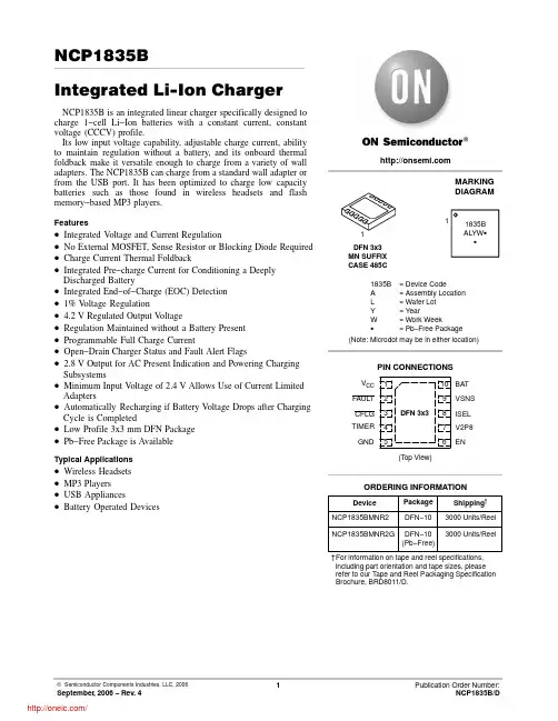
NCP1835BIntegrated Li−Ion ChargerNCP1835B is an integrated linear charger specifically designed to charge 1−cell Li−Ion batteries with a constant current, constant voltage (CCCV) profile.Its low input voltage capability, adjustable charge current, ability to maintain regulation without a battery, and its onboard thermal foldback make it versatile enough to charge from a variety of wall adapters. The NCP1835B can charge from a standard wall adapter or from the USB port. It has been optimized to charge low capacity batteries such as those found in wireless headsets and flash memory−based MP3 players.Features•Integrated V oltage and Current Regulation•No External MOSFET, Sense Resistor or Blocking Diode Required •Charge Current Thermal Foldback•Integrated Pre−charge Current for Conditioning a Deeply Discharged Battery•Integrated End−of−Charge (EOC) Detection•1% V oltage Regulation•4.2 V Regulated Output V oltage•Regulation Maintained without a Battery Present •Programmable Full Charge Current•Open−Drain Charger Status and Fault Alert Flags•2.8 V Output for AC Present Indication and Powering Charging Subsystems•Minimum Input Voltage of 2.4 V Allows Use of Current Limited Adapters•Automatically Recharging if Battery Voltage Drops after Charging Cycle is Completed•Low Profile 3x3 mm DFN Package•Pb−Free Package is AvailableTypical Applications•Wireless Headsets•MP3 Players•USB Appliances•Battery Operated DevicesDevice Package Shipping†ORDERING INFORMATIONNCP1835BMNR2DFN−103000 Units/Reel†For information on tape and reel specifications, including part orientation and tape sizes, please refer to our T ape and Reel Packaging Specification Brochure, BRD8011/D.NCP1835BMNR2G DFN−10(Pb−Free)3000 Units/ReelFigure 1. Typical 50 mA Application CircuitPIN FUNCTION DESCRIPTIONPin Symbol Description1V CC Input Supply Voltage. Provides power to the charger. This pin should be bypassed with at least a 4.7 m F ceramic capacitor to ground.2FAULT An open−drain output indicating fault status. This pin is pulled LOW under any fault conditions. A FAULT condition resets the counter.3CFLG An open−drain output indicating charging or end−of−charge states. The CFLG pin is pulled LOW when the charger is charging a battery. It is forced open when the charge current drops to I EOC. This high impedance mode will belatched until a recharge cycle or a new charge cycle starts.4TIMER Connecting a timing capacitor, C TIME between this pin and ground to set end−of−charge timeout timer.TIMEOUT = 14*C TIME/1.0 nF (minute). The total charge for CC and CV mode is limited to the length of TIMEOUT.Trickle Charge has a time limit of 1/8 of the TIMEOUT period.5GND Ground pin of the IC. For thermal consideration, it is recommended to solder the exposed metal pad on the back-side of the package to ground.6EN Enable logic input. Connect the EN pin to LOW to disable the charger or leave it floating to enable the charger.7V2P8 2.8 V reference voltage output. This pin outputs a 2.8 V voltage source when an adapter is present. The maximum loading for this pin is 2.0 mA.8ISEL The full charge current (I FCHG) can be set by connecting a resistor, R ISEL, from the ISEL pin to ground.For best accuracy, a resistor with 1% tolerance is recommended.9VSNS Battery voltage sense pin. Connect this as close as possible to the battery input connection.10BAT Charge current output. A minimum 4.7 m F capacitor is needed for stability when the battery is not attached.Figure 2. Detailed Block DiagramVSNSBATISELEN GNDTIMER MAXIMUM RATINGSRatingSymbol Value Unit Supply Voltage V CC 7.0V Status Flag Output Pins V FAULT , V CFLG7.0V Voltage Range for Other Pins V io 5.5V Current Out from BAT PinI O 1.2A Thermal CharacteristicsThermal Resistance, Junction−to−Air (Note 3)Power Dissipation, T A = 25°C (Note 3)R q JA P D 68.51.09°C/W WMoisture Sensitivity (Note 4)MSL Level 1Operating Ambient T emperature T A −20 to 70°C Storage T emperature T stg −55 to 125°C ESDHuman Body Model Machine ModelHBM MM2000200V V Stresses exceeding Maximum Ratings may damage the device. Maximum Ratings are stress ratings only. Functional operation above the Recommended Operating Conditions is not implied. Extended exposure to stresses above the Recommended Operating Conditions may affect device reliability.1.This device series contains ESD protection and is tested per the following standards:Human Body Model (HBM) per JEDEC standard: JESD22−A114.Machine Model (MM) per JEDEC standard: JESD22−A115.tchup Current Maximum Rating: 150 mA per JEDEC standard: JESD78.3.Measure on 1 inch sq. of 1 oz. copper area. R q JA is highly dependent on the PCB heatsink area. For example, R q JA can be 38°C/W on 1 inch sq. of 1 oz. copper area on 4 layer PCB that has 1 single signal layer with the additional 3 solid ground or power planes. The maximum package power dissipation limit must not be exceeded:P D +T J(max)*T AR q JAwith R q JA = 68.5°C/W, T J(max) = 100°C, P D = 1.09 W.4.Moisture Sensitivity Level per IPC/JEDEC standard: J−STD−020A.ELECTRICAL CHARACTERISTICS (Typical values are tested at V CC = 5.0 V and room temperature, maximum and minimum values are guaranteed over 0°C to 70°C with a supply voltage in the range of 4.3 V to 6.5 V, unless otherwise noted.)Characteristic Symbol Min Typ Max Unit V CC SUPPLYOperating Supply Range V CC 2.8− 6.5V Rising V CC Threshold V RISE 3.0 3.4 3.95V Falling V CC Lockout Threshold V FALL 2.0 2.4 2.8V Quiescent V CC Pin Supply CurrentShutdown (EN = Low) Normal Operation (EN = High)I VCCI VCC−−30600−−m Am ABattery Drain CurrentManual Shutdown (V CC = 5.0 V, VSNS = 4.0 V, EN = Low)I BMS−− 3.0m ACHARGING PERFORMANCERegulated Output Voltage in Constant Voltage (CV) Mode, I CHG = 10 mA V REG 4.158 4.200 4.242V Dropout Voltage (V BAT = 3.7 V, I CHG = 0.1 A)−−80120mV Pre−Charge Threshold Voltage V PC 2.52 2.8 3.08V Pre−Charge Current (R ISEL = 2.7 M W, V BAT = 2.0 V)I PC 1.02030mA Pre−Charge Current (R ISEL = 270 k W, V BAT = 2.0 V)I PC305065mA Recommended Full Charge Current I FCHG30−300mA Full−Charge Current in Constant Current (CC) Mode (R ISEL = 2.7 M W, V BAT = 3.7 V)I FCHG304558mA Full−Charge Current in Constant Current (CC) Mode (R ISEL = 270 k W, V BAT = 3.7 V)I FCHG280310360mA End−of−Charge Threshold (R ISEL = 2.7 M W, V BAT = V REG)I EOC 1.0 4.011mA End−of−Charge Threshold (R ISEL = 270 k W, V BAT = V REG)I EOC263442mA Recharge Voltage Threshold V RECH 3.80 4.03 4.155V Thermal Foldback Limit (Junction T emperature) (Note 5)T LIM−100−°C OSCILLATOROscillation Period (C TIME = 15 nF)T OSC 2.4 3.0 3.6ms4.55.0 5.56.0 6.5V CC , INPUT VOLTAGE (V)V 2P 8, V 2P 8 V O L T A G E (V )V R E G , R E G U L A T E D O U T P U T V O L T A G E (V )Figure 5. Regulated Output Voltage vs.TemperatureFigure 6. ISEL Voltage vs. Input VoltageFigure 7. V2P8 Voltage vs. Input Voltage−50−25255075T A , AMBIENT TEMPERATURE (°C)V R E G , R E G U L A T E D O U T P U T V O L T A G E (V )1001254.55.05.56.06.5V CC , INPUT VOLTAGE (V)2.53.03.54.04.5V BAT , BATTERY VOLTAGE (V)V 2P 8, V 2P 8 V O L T A G E (V )I P C , T R I C K L E C H A R G E C U R R E N T (m A )4.55.05.56.06.5V CC , INPUT VOLTAGE (V)V R E C H , R E C H A R G E V O L T A G E (V )Figure 12. Recharge Voltage vs. Input Voltage Figure 13. Charge Current vs. Battery VoltageDETAILED OPERATING DESCRIPTIONOverviewRechargeable Li−Ion/Polymer batteries are normally charged with a constant current (CC) until the terminal voltage reaches a fixed voltage threshold, at which point a constant voltage (CV) is applied and the current drawn by the battery decays. The charging rate is determined by the specific rating of the battery. For example, if the battery is rated at 800 mA−hours, then the recommended maximum charge rate is 800 mA. For a severely discharged cell, it takes approximately 2.5−3.5 hours to recharge the battery at the maximum rate. So, when one charges at less than the maximum charge rate, the recharge time increases. Also, the battery should not be continuously charged or the battery could age faster than necessary. Because of this, Li−Ion charging systems need to stop charging within a prescribed time limit regardless of the charge rate.The NCP1835B is a fully integrated, stand−alone 1−cell Li−Ion charger which performs the primary battery charging functions and includes a timer which will terminate charging if the battery has not completed charging within a prescribed time period. The charging rate is user programmable up to 1.0 A and the end−of−charge timer is also programmable. The NCP1835B has a thermal foldback loop which reduces the charge rate if the junction temperature is exceeded. The device also includes several outputs which can be used to drive LED indicators or interface to a microprocessor to provide status information. The adapter providing power to the charger can be a standard fixed output voltage such as a 5.0 V wall adapter or it can be a simple current limited adapter.The NCP1835B comes in two versions with output voltage regulation thresholds of 4.2 or 4.242 V depending on the requirements of the specific battery pack being used. The user determines the charge current by selecting the resistor R ISEL and determines the length of the end−of−charge timeout timer by selecting the capacitor, C TIME.Charging OperationFigure 13 outlines the charging algorithm of the NCP1835B and Figure 14 graphically illustrates this. When the charger is powered up and the input voltage rises above the power−on, rising threshold (nominally 3.4 V), the charger initiates the charging cycle.The NCP1835B first determines the cell voltage. If it is less than the pre−charge threshold (2.8 V), the IC recognizes the battery as severely discharged. In this state, the NCP1835B pre−conditions (trickle charges) the battery by charging it at 10% of the full charge rate (I PC). This slow charge prevents the battery from being damaged from high fast charge currents when it is in a deeply discharged state. The battery voltage should be trickle charged up to 2.8 V before 1/8 of the preset end−of−charge time is expired. If it cannot reach this voltage, than the battery is possibly shorted or damaged. Therefore, the NCP1835B stops charging and the pre−charge timeout signal asserts the FAULT flag.Once the cell voltage crosses the pre−charge threshold, the device will transition to normal (full−rate) charging at 100% of the programmed full rate charge current (I FCHG). As the NCP1835B charges the battery, the cell voltage rises until it reaches the V REG threshold, (4.2 or 4.242 V). At the maximum charge rate, it normally takes about 1 hour to reach this point from a fully discharged state, and the battery will be approximately 70−80% recharged. At this point, the charge transitions to constant voltage mode where the IC forces the battery to remain at a constant voltage, V REG. During this constant voltage state, the current required to maintain V REG steadily decreases as the battery approaches full charge. Charge current eventually falls to a very low value as the battery approaches a fully charged condition.The NCP1835B monitors the current into the battery until it drops to 10% of the full charge rate. This is the End−of−Charge (EOC) threshold. Normally it takes 1.5−2.5 hours to reach this point. Once the NCP1835B reaches end−of−charge it opens the CFLG pin and enters the EOC state. The IC continues to charge the battery until it reaches TIMEOUT. At that point, the NCP1835B stops charging. If the system does not reach EOC during the TIMEOUT period, the NCP1835B views this as a system drops below the recharge threshold (which can occur if the battery is loaded), the IC reinitializes the charging sequence and begins a new charge cycle. The recharge voltage threshold, V RECH, is nominally 4.03 V.In the inhibit state, the NCP1835B continues to monitor the battery voltage, but does not charge the battery. Again, if the battery voltage drops below the recharge threshold the IC reinitializes the charging sequence and begins a new charge cycle.Figure 15. Typical Charging DiagramTrickleCC CV End ofTimeTimeTimeTimeTimeTimeTable 1. Charge StatusConditionCFLG FAULT Trickle, Constant Current and Constant Voltage Charge Low High End−of−Charge or Shutdown ModeHigh High Timeout Fault, V ISEL < 0.35 V or V ISEL > 1.4 VHighLowCharge Status Indicator (CFLG)CFLG is an open−drain output that indicates battery charging or End−of−Charge (EOC) status. It is pulled low when charging in constant current mode and constant voltage mode. It will be forced to a high impedance state when the charge current drops to I EOC. When the charger is in shutdown mode, CFLG will also stay in the high impedance state.Fault Indicator (FAULT)FAULT is an open−drain output that indicates that a charge fault has occurred. It has two states: low or high impedance. In a normal charge cycle, it stays in a high impedance state. At fault conditions, it will be pulled low and terminate the charge cycle. A timeout fault occurs when the full charge or pre−charge timeouts are violated, or if the voltage on ISEL is greater than 1.4 V or lower than 0.35 V. There are two ways to get the charger out of a fault condition and back to a normal charge cycle. One can either toggle the EN pin from GND to a floating state or reset the input power supply.Adapter Present Indicator (V2P8)V2P8 is an input power supply presence indicator. When the input voltage, V CC, is above the power on threshold (V RISE, nominally 3.4 V) and is also 100 mV above the battery voltage, it provides a 2.8 V reference voltage that can source up to 2.0 mA. This voltage can also be used to power a microprocessor I/O.Enable/Disable (EN)Pulling the EN pin to GND disables the NCP1835B. In shutdown mode, the internal reference, oscillator, and control circuits are all turned off. This reduces the battery drain current to less than 3.0 m A and the input supply current to 30 m A. Floating the EN pin enables the charger. Thermal FoldbackAn internal thermal foldback loop reduces the programmed charge current proportionally if the die temperature rises above the preset thermal limit (nominally 100°C). This feature provides the charger protection from over heating or thermal damage. Figure 16 shows the full charge current reduction due to die temperature increase across the thermal foldback limit. For a charger with a 1.0 A constant charge current, the charge current starts decreasing when the die temperature hits 100°C and is reduced to zero when the die temperature rises to 110°C.Figure 16. Full Charge Current vs. JunctionTemperatureICHG,CHARGECURRENTT J, JUNCTION TEMPERATURE分销商库存信息:ONSEMINCP1835BMNR2NCP1835BMNR2G。