ccd器件技术手册
- 格式:pdf
- 大小:6.42 MB
- 文档页数:76

CCD说明书视频图象测量仪产品总述本产品可用于高精度测量,实现视频信号的数据处理,完成距离、角度的测量工作。
产品特点操作简单按钮控制、旋钮控制、鼠标控制高工作效率数据实时刷新,无须等待,工作稳定测量方式横向距离、纵向距离、任意两点之间距离任意3点所确定的圆的半径任意3点所确定的圆的角度任意设定单位距离任意设定中心位置任意设定初始工作模式两种显示位置选择主要参数输入制式NTSC : 1.0V p-p 75ΩPAL : 1.0V p-p 75Ω分辨率水平 500 垂直 230测量精度最大电气信号处理精度:水平1/500 垂直1/230 角度 0.1°(计算精度)最大显示值距离:99.99mm 角度:360.0°显示模式两种数据显示模式电源输入DC12V 1.5A 请使用专用开关电源工作温度-10℃~70℃外型尺寸重量制造商南京涉谷电子束技术有限公司 TEL:使用说明安装1将随机附带的12V1.5A的开关电源接入DC IN圆形电源插孔,将视频输入信号接入VIDEO IN视频插座,将VIDEO OUT视频插座与显示器相连,将鼠标接入MOUSE接口注意:DC OUT能够提供12V 1A的输出。
鼠标能够不连接,但若要使用鼠标请必须在开机前接入!2 接通电源,打开显示器,将测试仪POWER开关向上拨动,红色电源指示灯亮,测试仪开始工作,显示器显示工作界面图1(前面板)图2(后面板)初始设置按住MODE键开机或者RESET,便可出现初始设置界面(如图3所示),经过鼠标或者SELECT键选择所要设置的选项,选择完毕之后经过鼠标左键或者SET键确定便可进入相应的设置界面。
图3*初始位置设置界面(如图4所示)图4经过鼠标或者X、Y CURSOR旋钮移动横竖坐标线到所需位置,按鼠标右键或者SET键便可完成设置回到初始画面*矫正设置界面(如图5、6所示)图5图6经过SELECT键选择单位,能够为mm/um经过鼠标或者X、Y CURSOR旋钮移动横竖坐标线,此时实线的交点和虚线的交点之间的距离即为1mm/1um,能够经过鼠标左键实现实线和虚线位置的交换,按鼠标右键或者SET键便可完成设置回到初始画面*初始工作模式选择界面(如图7所示)图7经过鼠标或者SELECT键选择相应的工作模式,按鼠标左键完成设置回到初始画面*数据显示位置选择界面(如图8、9所示)图8图9 经过鼠标或者SELECT键选择相应的数据显示位置,按鼠标右键或者SET键便可完成设置回到初始画面初始设置完成经过START键开始工作,设置将会被保存,开机自动应用工作模式进入工作模式之后,初始状态即为初始设置的方式*测量横向距离、纵向距离、任意两点之间距离界面(同图8所示)经过鼠标或者X、Y CURSOR旋钮移动横竖坐标线,此时X的值为横向距离,Y的值纵向距离D的值为实线的交点和虚线的交点之间的距离,能够经过鼠标左键或者点触X、Y CURSOR旋钮实现实线和虚线位置的交换*任意3点所确定的圆的半径界面(如图10所示)图10经过鼠标或者X、Y CURSOR旋钮移动横竖坐标线,此时X的值为横向距离,Y的值为纵向距离,D的值为实线的交点和虚线的交点之间的距离,经过鼠标左键或者点触X、Y CURSOR旋钮选定第一个点,此时虚线的交点便会移动到第一点的位置,然后再经过鼠标左键或者点触X、Y CURSOR旋钮选定第二个点(注意:第二个点没有显示),最后再经过鼠标左键或者点触X、Y CURSOR旋钮选定第三个点,此时R的值为任意3点所确定的圆的半径的值*任意3点所确定的圆的角度界面(如图11所示)图11经过鼠标或者X、Y CURSOR旋钮移动横竖坐标线,此时X的值为横向距离,Y的值为纵向距离,D的值为实线的交点和虚线的交点之间的距离,经过鼠标左键或者点触X、Y CURSOR旋钮选定第一个点,此时虚线的交点便会移动到第一点的位置,然后再经过鼠标左键或者点触X、Y CURSOR旋钮选定第二个点(注意:第二个点没有显示),最后再经过鼠标左键或者点触X、Y CURSOR 旋钮选定第三个点,此时R的值为任意3点所确定的角的角度值(以第二点为顶点)*十字线模式界面(同图4所示)*纯视频输出模式工作模式转换经过鼠标右键或者MODE键进入模式选择界面(同图7所示)经过鼠标或者SELECT键选择相应的模式,按鼠标右键或者SET键便可完成设置回到工作模式经过拨动DISPLAY开关,能够实现显示亮度的转换。
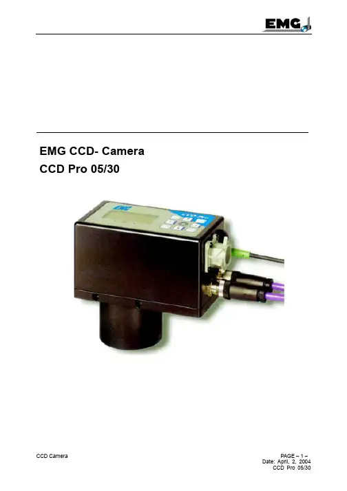
操作手册EMG CCD- CameraCCD Pro 05/30本手册所用到的符号:警示符号: 在本手册中使用以明确的分别不同的重要场合小心:必须注意这类警示,操作者要小心机械运动可能带来的人身伤害。
危险:在操作这些设备时必须小心,不允许误操作,高电压可能造成较大的伤亡事故。
注意:这些符号指示的是一些有用的帮助或附加功能。
目录本手册中使用的符号 (2)警示符号 (2)目录 (3)1. 概述 (4)1.1 说明 (4)1.2 使用场合 (4)1.3 安全信息 (5)1.4 噪音 (5)2. 显示及操作控制 (6)2.1 检测器控制面板 (6)2.2 连接 (7)3. 菜单 (8)3.1 数字输入 (8)3.2 底脚目录行 (9)3.2.1 菜单向导 (9)3.2.2 菜单行和边缘参数标志 (9)3.3 设定菜单 (11)3.3.1 菜单向导 (11)3.3.2 菜单层次 (12)4. 集成/安装 (13)4.1 安装要求 (13)4,2 安装检测器 (13)4.3 安装光源 (13)4.4 背景定义 (14)4.5 安装支撑辊 (14)4.6 安装 (14)5. 调试 (15)5.1 CAN Bus地址和终端设定 (15)5.2 机械校准 (16)5.2.1 粗调 (16)5.2.2 精调 (18)5.3 检测器配置 (22)5.3.1 亮度转换的定义 (25)5.4 CCD检测器同步PDO数据传输的编程 (25)6. 操作 (26)6.1 图形显示 (26)6.2 在操作中改变设置 (27)6.2.1 语言设置 (27)6.2.2 总线信息 (27)6.2.3 设置默认值 (27)7 维护保养 (28)8 技术规格 (29)8.1 CCD检测器测量范围/距离 (30)9 运输/储存 (31)10 拆除 (31)1. 概述1.1 说明本手册适用于所有的CCD Pro…model CCD检测器。
本手册介绍采用一个或两个CCD检测器,应用在板带纠偏或板带宽度测量的场合。
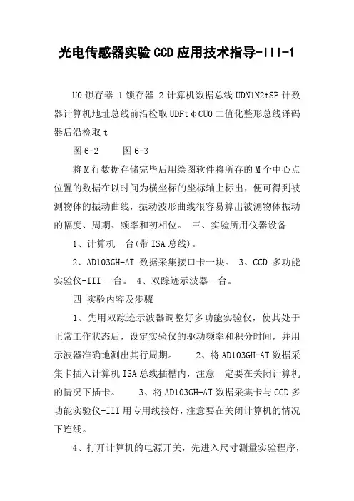
光电传感器实验CCD应用技术指导-III-1U0锁存器 1锁存器 2计算机数据总线UDN1N2tSP计数器计算机地址总线前沿检取UDFtφCU0二值化整形总线译码器后沿检取t图6-2 图6-3将M行数据存储完毕后用绘图软件将所存的M个中心点位置的数据在以时间为横坐标的坐标轴上标出,便可得到被测物体的振动曲线,振动波形曲线很容易算出被测物体振动的幅度、周期、频率和初相位。
三、实验所用仪器设备1、计算机一台(带ISA总线)。
2、AD103GH-AT数据采集接口卡一块。
3、CCD多功能实验仪-III一台。
4、双踪迹示波器一台。
四实验内容及步骤1、先用双踪迹示波器调整好多功能实验仪,使其处于正常工作状态后,设定实验仪的驱动频率和积分时间,并用示波器准确地测出其行周期。
2、将AD103GH-AT数据采集卡插入计算机ISA总线插槽内,注意一定要在关闭计算机的情况下插卡。
3、将AD103GH-AT数据采集卡与CCD多功能实验仪-III用专用线接好,注意要在关闭计算机的情况下连线。
4、打开计算机的电源开关,先进入尺寸测量实验程序,测出实验板的缝宽,2mm或3mm。
5、进入物体振动实验程序。
进入程序后,请按菜单提示要求进行操作,首先设置所要测量的波形的测量点数M;再设置二值化阈值电平Uth之后,用手沿平行于多功能实验仪CCD入射窗的方向摆动实验板窄缝,产生振动的光信号。
然后执行振动测量程序,经过一段时间的采集后,计算机将自动地显示实验板窄缝的振动波形,从波形上可以分析计算出其振幅、频率和初相位。
五实验结果及实验报告实验完成后,将计算机所测得的数据打印出来,以时间为横坐标,以1048像元值为纵坐标的零点,将测得的每个数据标在这个坐标轴上,便可得到所测得的振动波形,再与计算机画出的波形相比较。
写出这个实验的心得体会。
16171819实验八面阵CCD实验面阵CCD是当前应用最广泛的CCD器件,它常被用于监控系统、保安、防范、交通指挥、摄录像和数码照相等领域。
5.7作废
当有更改后的技术文件批准发布时,文件制定部门应用开发电路Part及文件接收部门,均以最终版本的文件为准,上一版本的旧文件自行作废。
但应用开发电路Part部门保留一份上一版本旧版本电子版文件,以备参考。
书面保存的作废文件必须要加盖作废图章。
5.8保管:分为电子版保存和书面保存
5.8.1 应用开发电路Part制定的技术文件,通常由文件制定人保存电子版本。
5.8.2 无法采用电子版本或必须使用书面以及需要书面参考文件时,采用打印的书面文件。
保管下发的书面技术文件要有《技术文件分发履历书》,将文件资料按类别进行统计
以便进行管理。
5.9外来文件
外来文件(包括产品标准,韩文型号特性等文件)无需审批,视为本公司文件。
应用开发电路Part即时整理外来文件,根据需要进行保管或是废弃。
所有文件保留电子版本,应保持清晰、易于识别和检索。
由韩国本社负责跟踪产品技术质量有关的国家、行业标准的更新信息,确保公司适用最新的有效版本。
6.相关文件
CCD4-0011C 型号特性编制作业指示书管理规则
7.附录
[技术文件分发履历书]
[受控文件图章样式] [作废图章样式]。
Whilst e2v technologies has taken care to ensure the accuracy of the information contained herein it accepts no responsibility for the consequences of any use thereof and also reserves the right to change the specification of goods without notice. e2v technologies accepts no liability beyond the set out in its standard conditions of sale in respect of infringement of third party patents arising from the use of tubes or other devices in accordance with information contained herein.e2v technologies limited, Waterhouse Lane, Chelmsford, Essex CM1 2QU United Kingdom Telephone: +44 (0)1245 493493 Facsimile: +44 (0)1245 492492e-mail: enquiries@ Internet: Holding Company: e2v technologies plce2v technologies inc. 4 Westchester Plaza, PO Box 1482, Elmsford, NY10523-1482 USA Telephone: (914) 592-6050 Facsimile: (914) 592-5148 e-mail: enquiries@INTRODUCTIONThe CCD55-30 is one of the CCD55 range of large area image sensors primarily intended to suit the requirements of astronomy, medical diagnostic and scientific measuring instruments. The device utilises Advanced Inverted-Mode Operation (AIMO) for lowest dark current. It operates with standard three-phase clocking and buried channel charge transfer. The read-out register has a low-noise amplifier at one end for slow-scan applications and a high speed amplifier at the other end.DESCRIPTIONThe sensor has an image area with 1252 x 1152 pixels for Full Frame variants. Frame Transfer variants can also be produced by application of a metal “store shield” leaving an unobstructed image area of 1242 x 574 usable pixels. There is a single output register that has charge detection circuits incorporated at each end. One output (A1) is intended for high-speed operation and has an associated dummy output circuit. By design the maximum speed of this output is approximately 6 MHz, as set by being sufficiently settled for reliable CDS with ≤10 pF load, but operation up to 9 MHz should be achievable if incomplete settling can be tolerated. This output is designed to have charge handling capacity of at least two image pixels. The second output (A2) is designed for lower noise performance whilst still being able to handle the full well capacity of one pixel and by design has a maximum speed of approximately 3 MHz.VARIANTSMultiple AR coatings are available as well as the choice between Full Frame and Frame Transfer variants. Attachment of permanent windows is also an option and should be discussed directly with e2v.Non-inverted-mode options (N I MO) and other formats (e.g. CCD55-20) can also be provided and are described in other data sheets.Consult e2v technologies for any further information.The device pictured is without a store shield.SUMMARY SPECIFICATIONNumber of usable image pixels 1242 (H) x 574 (V)Read-out noise A1 6.5 e at 18.5 kHz−Quoted performance parameters given here are “typical” values. Specification limits are shown later.CCD55-30 AIMO Back Illuminated High Performance CCD SensorPERFORMANCEElectro-Optical SpecificationNote 1 Min Typical Max Units Note Peak charge storage (image) 400,000 e−/pixel 2,3Peak charge storage (register) 1,300,000 e−/pixel 2,3Output node capacity A1 1,300,000 e−2,3 A2 600,000 e−Output amplifier responsivity A1 0.8 1.2 1.6 µV/e−A2 2 3 4 µV/e−Read-out noise A1 6.5 e− rms4 A2 3.5 5 e− rmsDark signal at 273 K 70 110 e−/pixel/s5 at 293 K 800 1300 e−/pixel/sDark Signal Non-Uniformity at 273 K 30 53 e−/pixel/s5 at 293 K 185 325 e−/pixel/sCharge transfer efficiencyserial 99.9999 %2,6 parallel 99.9993 %NOTES1. Device performance will be within the limits specified by “max” and “min” when operated at the recommended voltagessupplied with the test data and when measured at a typical register clock frequency of 50 kHz. Performance at higher readout frequencies is not measured for production testing at e2v. The readout frequency for noise is defined separately in note 3.2. Typical values are provided from results of previous measurement or by design and by default are not measured per device.3. Signal level at which resolution begins to degrade.4. Measured at 253 K with an 18.5 kHz readout frequency.5. Dark signal (or current) is measured with the substrate voltage at +9V and the device temperature 273 K. It is a strongfunction of temperature and the typical AIMO average dark current Q d any temperature T (Kelvin) between 230 K and 300 K is given by:Q d/Q do = 1.14x10⁶T³e -9080 /Twhere Q do is the dark current at 293 K.Note, DSNU scales with temperature generally following the NIMO scaling of Q d/Q do = 122T³e -6400 /T.Transfer through the image sections can give rise to an additional temperature-independent signal component called “clock-induced charge” The CIC generated depends on the bias levels used, whether the device operates in inverted or non-inverted mode, and the details of the clock timings employed. Further details can be found on the e2v website or by contacting e2v.6. The CTE value is quoted for the complete clock cycle (i.e. all phases). If fitted, the permanent window on Frame Transfervariants would hamper CTE measurements. If it were to be measured, the reported results may under-estimate the true CTE performance.COSMETIC SPECIFICATIONSMaximum allowed defect levels are indicated below.Grade0 1 2 Column defects Black 0 2 6 White0 0 2 White spots 80 100 150 Black spots 50 100 400 Traps > 200e −2512Grade 5 devices are fully functional but with an image quality below that of grade 2, and may not meet all other specifications. Not all parameters may be tested.DEFINITIONSWhite spotsA defect is counted as a white spot if the dark generation rate is 50 times the specified maximum dark signal generation rate at 293 K. The typical temperature dependence of white spot defects is different from the average dark signal and is given by:Q d /Q do = 122T³e -6400/TBlack spots A black spot defect is a pixel with less than 80% of the local mean at a signal level of approximately half full well.Column defects A column is counted as a defect if it contains at least 9 white or dark single pixel defects. TrapsA trap causes charge to be temporarily held in a pixel and these are counted as defects ifthe quantity of trapped charge is greater than 200 e - at the specified test temperature (nominally 273 K).TYPICAL OUTPUT AMPLIFIER NOISEThe theoretical variation of typical read noise with operating frequency is shown below, if measured using correlated double sampling with a pre-sampling bandwidth equal to twice the pixel rate at approximately 253 K.SPECTRAL RESPONSE AT 253 K (−20 °C)Wavelength(nm)Minimum QE (%)Maximum Pixel Response Non-UniformityPRNU (1σ) (%)Basic Process Mid Band CoatedBasic Process Broad Band CoatedBasic ProcessUncoated [7]350 15 25 10 - 400 40 55 25 3 500 85 75 55 - 650 85 75 50 3 9003030305NOTE7. Only available in Full Frame format.TYPICAL QE VALUES FROM MODEL CALCULATIONModel inputs: Basic back thinning process, temperature -20 °C, silicon thickness 16.00 µm, typical AR coating layer thickness, incoherent reflection.NOTES8 Manufacturing process variation can mean actual sensor QE performance may differ from the typical values in these curves,but will meet minimum QE values from the spectral response table above. QE measurements are averaged over many pixels and over the pass band of the optical filter. 9 The values here represent performance at -20 °C. QE at longer wavelengths will decrease at much lower temperatures andincrease when temperature rises. Contact e2v for more information.DEFINITIONSBack-ThinningA back-thinned CCD is fabricated on the front surface of the silicon and is subsequently processed for illumination from the reverse side. This avoids loss of transmission in the electrode layer (particularly significant at shorter wavelengths or with low energy X-rays). This process requires the silicon to be reduced to a thin layer by a combination of chemical and mechanical means. The surface is “passivated” and an anti-reflection coating may be added.AR CoatingAnti-reflection coatings are normally applied to the back illuminated CCD to further improve the quantum efficiency. Standard coatings optimise the response in the visible, ultra-violet or infrared regions. For X-ray detection, an uncoated device may be preferable.Inverted Mode (IMO)An inverted mode CCD has an additional implant that allows charge integration to be carried out with all clock phases low. With a high voltage applied to the substrate (typically +9 V) this causes the whole of the device to be flooded with holes (inverted or pinned), which suppresses the surface component of dark signal. This leaves only the much lower bulk component, reducing the overall dark signal by a factor of approximately 100.Inverted mode operation is also referred to as multi-phase pinning (MPP).Readout NoiseReadout noise is the random noise from the CCD output stage in the absence of signal. This noise introduces a random fluctuation in the output voltage that is superimposed on the detected signal.The method of measurement involves reverse-clocking the register and determining the standard deviation of the output fluctuations, and then converting the result to an equivalent number of electrons using the known amplifier responsivity. Dummy OutputOutput A1 has an associated “dummy” circuit on-chip, which is of identical design to the “real” circuit but receives no signal charge. The dummy output should have the same levels of clock feed-through, and can thus be used to suppress the similar component in the “real” signal output by means of a differential pre-amplifier. The penalty is that the noise is increased by a factor of √2. If not required the dummy outputs may be powered down.Dark SignalThis is the output signal of the device with zero illumination. This typically consists of thermally generated electrons within the semiconductor material, which are accumulated during signal integration. Dark signal is a strong function of temperature as described in note 5.Correlated Double SamplingA technique for reducing the noise associated with the charge detection process by subtracting a first output sample taken just after reset from a second sample taken with charge present.Charge Transfer EfficiencyThe fraction of charge stored in a CCD element that is transferred to the adjacent element by a single clock cycle. The charge not transferred remains in the original element, possibly in trapping states and may possibly be released into later elements. The value of CTE is not constant but varies with signal size, temperature and clock frequency.ARCHITECTUREDevice SchematicFrame Transfer Image AreaABD AØ3AØ2AØ1SS BØ1BØ2BØ3DD DGI OD2OS2RD2ØR2CØ2CØ3G 6789101112131415163451217181920212239383736353433323130294241404443282726252423ABD AØ3AØ2AØ1SS BØ1BØ2BØ3DGI G OD1OS1DOS1RD1ØR1CØ1OGOUTPUT CIRCUITSLarge Signal (A1)Low Noise (A2)NOTES10. The DC restoration circuitry requires a pulse at the start of line read-out, and this is automatically obtained by an internalconnection to the BØ3 image clock, as can be seen in the schematics.11. The external load on the large signal output is not critical, but can be 7.5 mA constant current supply or a 3.3 kΩ resistor Theamplifier output impedance is typically 250 Ω for A1.12. The external load on the low noise output is not critical, but can be 5 mA constant current supply or a 5 kΩresistor. Theamplifier output impedance is typically 400 Ω for A2.ELECTRICAL INTERFACECONNECTIONS, TYPICAL VOLTAGES AND ABSOLUTE MAXIMUM RATINGSNOTES13. Reset and the A and B section clock pulse low levels should be 0 ± 0.5 V. The C section clock pulse low level should be set1 V higher.14. Charge can be reverse-clocked into the drain at the top of the device. During this period of clocking, I G should be 13 ± 1 Vfor 12 V image clocks.15. Non-charge dumping level shown. For charge dumping, DG should be 13 ± 1 V for 12 V register clocks.16. The device has no anti-blooming but a drain bus is present above section A and must be biased to prevent charge injection.The isolation gate I G is positioned between this bus and the first AØ1 electrode.17. The substrate voltage may need to be adjusted within the range indicated to achieve correct inverted mode operation.18. Various guard diodes are connected to the output drains and bias must be maintained. It is not therefore possible to switchoff an unused amplifier.19. Do not connect to voltage supply but use an external load, note 8. With a 5 mA constant-current load, VOS ~ VRD + 6 V.The current through this pin must not exceed 20 mA. Permanent damage may result if, in operation, OS experiences short circuit conditions.20. Phase 2 for read-out through amplifier A2, phase 1 for read-out through amplifier A1.21. Phase 1 for read-out through amplifier A2, phase 2 for read-out through amplifier A1.22. Do not connect to voltage supply but use an external load, note 9. With a 7.5 mA constant-current load, VOS ~ VRD + 6V.The current through this pin must not exceed 20 mA. Permanent damage may result if, in operation, OS or DOS experience short circuit conditions.PIN CONNECTIONS (View facing underside of package)ELECTRICAL INTERFACE CHARACTERISTICSElectrode Capacitances (calculated at mid-clock level)The total load to be driven per phase is the sum of the capacitance of the phase to substrate plus the inter-phase capacitance to each of the adjacent phases. For the AØ1 and BØ1 phases the total is 26.6 nF, for the AØ2, AØ3, BØ2 and BØ3 phases the total is 14 nF and for all CØ phases the total is 355 pF.POWER UP/POWER DOWNWhen powering the device up or down, it is critical that any specified maximum rating is not exceeded. Specifically the voltage for the amplifier and dump drains must never be taken negative with respect to the substrate. Hence, since the substrate is to be operated at a positive voltage, then the drive electronics should have a switch-on sequence which powers up all the drains to their positive voltages before the substrate voltage starts to increase from zero.It is also important to ensure that excess currents (see notes 19 and 22) do not flow in the OS or DOS pins. Such currents could arise from rapid charging of a signal coupling capacitor or from an incorrectly biased DC-coupled preamplifier.Similarly, for powering down, the substrate must be taken to zero voltage before the drains.POWER CONSUMPTIONThe power dissipated within the CCD is a combination of the static dissipation of the amplifiers and the dynamic dissipation from the parallel and serial clocking (i.e. driving the capacitive loads).The table below gives calculated values for the components of the power dissipation for different frame rates. The frequency is that for clocking the serial register. The clock period for parallel transfer is taken to be 20 µs (near the minimum).The amplifier power dissipation is the on-chip component for both A1 and A2. The clocked power dissipation is distributed between the device and the clock buffers.The dissipation reduces to only that of the amplifiers during any time that charge is being collected in the image sections with both the parallel and serial clocks static.TIMING DIAGRAMDETAIL OF LINE TRANSFERNote: For Full Frame readout, IØ = AØ = BØ. For Frame Transfer, IØ = BØ whilst AØ is low for charge collection.DETAIL OF OUTPUT CLOCKINGLINE OUTPUT FORMATCLOCK TIMING REQUIREMENTSThe table below details some limitations on the clock timing. Where no value is shown, the timing is either not critical or will be defined by the required readout rate.For AIMO operation, the first image electrode to be taken high after the all-low integrate phase should be Ø3 and the standard four pulse sequence, as shown in the detail of line transfer, is necessary to transfer a row to the register. For correct image row transfer, the voltage on the electrode should rise to at least 90% clock amplitude before the voltage on the previous phase electrode begins to fall. This in turn should reduce to below 10% clock pulse amplitude before the voltage on the next phase electrode begins to rise.For the register section, CØ1 and CØ2 should be high to receive charge from the last image row. The order of clock pulses to CØ1 and CØ2 determine the direction of readout to either A1 or A2, with A2 shown above by default.Symbol Description Min Typ Max UnitT i Image clock period15 3t op + 3t ip- µst wi Image clock pulse width8 2t op + 1t ip -t ri Image clock pulse rise time (10 to 90%)0.5 - 0.5t oiµst fi Image clock pulse fall time (10 to 90%)0.5 - 0.5t oiµst oi Image clock pulse overlap 3 - - µst li Image clock pulse, two phase low 2 - - µst dir Delay time, BØ stop to CØ start 3 - - µst dri Delay time, CØ stop to BØ start 1 - - µsT r Register clock period (note 23)150 - - nst rr Register pulse rise time (at 10-90% levels) 10 - 0.3T r nst fr Register pulse fall time (at 90-10% levels) 10 - 0.3T r nst or Register pulse overlap 10 - - nst wx Reset pulse width (at 50% levels) 20 - - nst rx, t fx Reset pulse rise and fall times 10 - - nsNOTE23 With the device pinned, the register clock overlaps required limit the maximum readout frequency to ~6 MHz for maximumcharge signal transfer, but faster operation could be possible for some loss in peak signal. At readout frequencies below the maximum it can be advantageous to use an asymmetrical timing, where, the CØ2 pulse can be minimised to only the width required to contain the reset pulse thereby maximising the reset and signal sampling windows.PACKAGE DETAILHANDLING CCD SENSORSCCD sensors, in common with most high performance MOS IC devices, are static sensitive. In certain cases, a discharge of static electricity may destroy or irreversibly degrade the device. Accordingly, full antistatic handling precautions should be taken whenever using a CCD sensor or module. These include: •Working at a fully grounded workbench•Operator wearing a grounded wrist strap•All receiving sockets to be positively groundedEvidence of incorrect handling will invalidate the warranty. All devices are provided with internal protection circuits to the gate electrodes (i.e. all CCD pins except SS, DD, RD, OD and OS) but not to the other pins.The devices are assembled in a clean room environment. e2v technologies recommend that similar precautions are taken to avoid contaminating the active surface.PART REFERENCESFor ordering information, some existing part numbers are below. Contact e2v for other variants.CCD55-30-*-xxx* = cosmetic gradexxx = device specific part numberPart Number DescriptionCCD55-30-*-348 Full Frame, Basic Midband, No Window CCD55-30-*-359 Full Frame, Basic Uncoated, No Window CCD55-30-*-S17 Full Frame, Basic Broadband, No WindowDimension Distance (mm) TolerancesA 53.34 ~ 1 %B 33.00 ~ 1 %C 2.54 -D 3.81 -E 2.3 ~ 10 %F <1.8 ~ 10 %G 43.18 ~ 1 %H 48.26 ~ 1 %The dimensions are provided for information.“E” is the thickness of the package at the greatest point where the temporary window sits on an outer ledge.HIGH ENERGY RADIATIONPerformance parameters will begin to change if the device is subject to ionising radiation. Characterisation data is held at e2v technologies with whom it is recommended that contact be made if devices are to be operated in any high radiation environment.TEMPERATURE RANGEOperating temperature range 153 - 323 KStorage temperature range 143 - 373 K Operation or storage in humid conditions may give rise to ice on the surface when the sensor taken to low ambient temperatures, thereby causing irreversible damage.Maximum rate of heating or cooling: 5 K/min.。