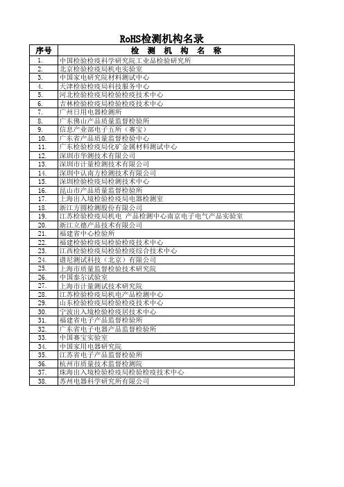
提交RoHS检 测报告供应商名录(第一
- 格式:pdf
- 大小:58.11 KB
- 文档页数:2
![供应商审核总结报告[1]](https://img.taocdn.com/s1/m/380f9729bcd126fff7050b8e.png)

FGQ-IV-08-8.3-08版本:A/0
产品型号:厂商型号:厂商批次:供应商批次:ERP进货单号:
生产日期:进货数量:送样部门:
检测日期:
1.检验部门尽量采集跟前期的检测数据,特别是经第三方检测确认过的批次的检测数据进行对比,或根据情况增加测试点的方式在检验环节做出风险确认;如果无法断定,请填写完整的检测数据和确认意见经部门领导批准签字后同时发给计划部,物料认证组和供管组;
2.计划部、物料认证组、供管组和预检四部门各委派一名成员组成RoHS检测(疑似)决议小组,预检成员要确保严格按RoHS同质材料的要求拆分检测,计划部成员准备其相关的产品的市场要求等信息,物料认证组成员要准备供应商提供的RoHS资料和前期的相关检测数据,供管组成员准备供应商的PCN协议、RoHS赔偿协议和承诺书等相关信息,于4小时的工作时之内共同给出当天的疑似物料的处理意见反馈给预检(特殊情况须向领导请示的除外)。
3.经决议需送第三方检测的,由物料认证组负责送检,供管组负责跟供应商协商付款过请款。
4.研发采购的物料RoHS检测的疑似情况由研发的RoHS评议小组进行判定,需送第三方检测的由物料认证组送检和请款。
注:本报告原始测试数据可见附件。
RoHS检验报告
样品名称:生产商/供应商:ERP品号:取样数量:
年 月 日
增加测试点的方给计划部,物料保严格按RoHS同的RoHS资料和前之内共同给出当
和请款。

广东华美骏达电器有限公司材料样品报告供 应H M J D-Q R-02.33A/2标识:3PEAK 1542A BCFe附图1 附图2附图3附图4在输入端输入方波信号,测量输出端的信号波形。
3PEAK1TP1541A/ TP1541NA/TP1542A/TP1544AStable 1.3MHz, Precision, RRIO, Op Amps Rev. B.04Features⏹ Stable 1.3MHz GBWP Over Temperature Range ⏹ Stable 1.3MHz GBWP in V CM from 0V to V DD ⏹ 0.7V/μs Slew Rate⏹ Only 80μA of Supply Current per Amplifier ⏹ Excellent EMIRR: 80dB(1GHz) ⏹ Offset Voltage: 400uV Maximum⏹ Offset Voltage Temperature Drift: 1uV/°C ⏹ Input Bias Current: 1pA Typical⏹ THD+Noise: -105dB at 1kHz, -90dB at 10kHz ⏹ High CMRR/PSRR: 95dB/90dB⏹ Beyond the Rails Input Common-Mode Range ⏹ High Output Current: 100mA⏹ No Phase Reversal for Overdriven Inputs ⏹ Drives 2kΩ Resistive Loads⏹ Shutdown Current: 0.2μA (TP1541NA) ⏹ Single +2.1V to +6.0V Supply Voltage Range ⏹ –40°C to 125°C Operation Temperature Range ⏹ ESD Rating:Robust 8KV – HBM, 2KV – CDM and 500V – MM ⏹Green, Popular Type PackageApplications⏹ Audio Output⏹ Active Filters, ASIC Input or Output Amplifier ⏹ Portable Instruments and Mobile Equipment ⏹ Battery or Solar Powered Systems ⏹ Smoke/Gas/Environment Sensors ⏹ Piezo Electrical Transducer Amplifier ⏹ Medical Equipment ⏹PCMCIA CardsDescriptionTP154xA series are CMOS single/dual/quad op-amps with low offset, stable high frequency response, low power, low supply voltage, and rail-to-rail inputs and outputs. They incorporate 3PEAK ‟s proprietary and patented design techniques to achieve best in-class performance among all micro-power CMOS amplifiers in its power class. The TP154xA family can be used as plug-in replacements for many commercially available op-amps to reduce power and improve input/output range and performance.TP154xA are unity gain stable with Any Capacitive load with a constant 1.3MHz GBWP, 0.7V/μs slew rate while consuming only 80μA of quiescent current per amplifier. Analog trim and calibration routine reduce input offset voltage to below 0.4mV, and proprietary precision temperature compensation technique makes offset voltage temperature drift at 1μV/°C. Adaptive biasing and dynamic compensation enables the TP154xA to achieve …THD+Noise ‟ for 1kHz/10kHz 2V PP signal at -105dB and -90dB, respectively. Beyond the rails input and rail-to-rail output characteristics allow the full power-supply voltage to be used for signal range. This combination of features makes the TP154xA ideal choices for battery-powered applications because they minimize errors due to power supply voltage variations over the lifetime of the battery and maintain high CMRR even for a rail-to-rail input op-amp. General audio output, remote battery- powered sensors, and smoke detector can benefit from the features of the TP154xA op-amps. For applications that require power-down, the TP1541NA in popular type packages has alow-power shutdown mode that reduces supply current to 0.2μA , and forces the output into a high-impedance state.3PEAK and the 3PEAK logo are registered trademarks of 3PEAK INCORPORATED. All other trademarks are the property of their respective owners.Pin Configuration (Top View)TP1541A5-Pin SOT23/SC70Out +In﹣Vs VsTP1542A8-Pin SOIC/TSSOP/MSOPOut A ﹢In A ﹣In A In BIn BOut B﹣VsVs TP1544A14-Pin SOIC/TSSOP﹢﹣In D In D ﹢﹣In C In CVs ﹢TP1541NA6-Pin SC70-V Out A﹢In A ﹣In A ﹣VsIn BIn B Vs TP1542A8-Pin DFN (-F Suffix)黄灼数字签名人 黄灼DN :cn=黄灼,c=CN-中国,o=华美骏达,ou=研发中心原因:我已审阅该文档日期:2017.02.1409:41:49 +08'00'2TP1541A/TP1541NA/TP1542A/TP1544AStable 1.3MHz, Precision, RRIO, Op AmpsRev. B.04 Absolute Maximum Ratings Note 1Supply Voltage: V +– V –....................................7.0V Input Voltage............................. V –– 0.3 to V ++ 0.3 Input Current: +IN, –IN, SHDN Note 2.............. ±10mA Differential Input Voltage................................ ±7VSHDN Pin Voltage ……………………………V – to V +Output Short-Circuit Duration Note 3…............ Infinite Operating Temperature Range.......–40°C to 125°C Maximum Junction Temperature................... 150°C Storage Temperature Range.......... –65°C to 150°C Lead Temperature (Soldering, 10 sec) ......... 260°CNote 1: Stresses beyond those listed under Absolute Maximum Ratings may cause permanent damage to the device. Exposure to anyAbsolute Maximum Rating condition for extended periods may affect device reliability and lifetime.Note 2: The inputs are protected by ESD protection diodes to each power supply. If the input extends more than 500mV beyond the power supply, the input current should be limited to less than 10mA.Note 3: A heat sink may be required to keep the junction temperature below the absolute maximum. This depends on the power supply voltage and how many amplifiers are shorted. Thermal resistance varies with the amount of PC board metal connected to the package. The specified values are for short traces connected to the leads.ESD, Electrostatic Discharge ProtectionOrder Information3TP1541A/TP1541NA/TP1542A/TP1544AStable 1.3MHz, Precision, RRIO, Op Amps Rev. B.04Electrical CharacteristicsThe specifications are at T A = 27°C. V S = 5V, V CM = 2.5V, R L = 2k Ω, C L =100pF, Unless otherwise noted.4Rev. B.04 5TP1541A/TP1541NA/TP1542A/TP1544AStable 1.3MHz, Precision, RRIO, Op Amps Rev. B.04Typical Performance CharacteristicsV S = ±2.75V, V CM = 0V, R L = Open, unless otherwise specified. (Continued)Common Mode Rejection Ratio CMRR vs. FrequencyQuiescent Current vs. Temperature Short Circuit Current vs. TemperaturePower-Supply Rejection RatioQuiescent Current vs. Supply Voltage6TP1541A/TP1541NA/TP1542A/TP1544AStable 1.3MHz, Precision, RRIO, Op AmpsRev. B.04 Typical Performance CharacteristicsV S = ±2.75V, V CM = 0V, R L = Open, unless otherwise specified. (Continued)PSRR vs. Temperature CMRR vs. TemperatureEMIRR IN+ vs. FrequencyLarge-Scale Step ResponseNegative Over-Voltage Recovery Positive Over-Voltage RecoveryTime (50μs/div)Gain = 1R L = 10k ΩTime (50μs/div)Gain = +10±V = ±2.5VTime (50μs/div)Gain = +10±V = ±2.5V7TP1541A/TP1541NA/TP1542A/TP1544AStable 1.3MHz, Precision, RRIO, Op Amps Rev. B.04Typical Performance CharacteristicsV S = ±2.75V, V CM = 0V, R L = Open, unless otherwise specified. (Continued)0.1 Hz TO 10 Hz Input Voltage NoiseOffset Voltage vs Common-Mode VoltagePositive Output Swing vs. Load Current Negative Output Swing vs. Load CurrentOffset Voltage vs. Temperature8TP1541A/TP1541NA/TP1542A/TP1544AStable 1.3MHz, Precision, RRIO, Op AmpsRev. B.04 Pin Functions–IN: Inverting Input of the Amplifier. Voltage rangeof this pin can go from V – – 0.3V to V ++ 0.3V. +IN: Non-Inverting Input of Amplifier. This pin has the same voltage range as –IN.+V S : Positive Power Supply. Typically the voltage is from 2.1V to 6V. Split supplies are possible as long as the voltage between V+ and V – is between 2.1V and 6V. A bypass capacitor of 0.1μF as close to the part as possible should be used between power supply pins or between supply pins and ground. -V S : Negative Power Supply. It is normally tied to ground. It can also be tied to a voltage other thanground as long as the voltage between V + and V –is from 2.1V to 6V. If it is not connected to ground, bypass it with a capacitor of 0.1μF as close to the part as possible.SHDN: Active Low Shutdown. Shutdown threshold is 1.0V above negative supply rail. If unconnected, the amplifier is automatically enabled.OUT: Amplifier Output. The voltage range extends to within millivolts of each supply rail.N/C: No Connection.OperationThe TP154xA family input signal range extends beyond the negative and positive power supplies. The output can even extend all the way to the negative supply. The input stage is comprised of two CMOS differential amplifiers, a PMOS stage and NMOS stage that are active over different ranges of common mode input voltage. The Class-AB control buffer and output bias stage uses a proprietary compensation technique to take full advantage of the process technology to drive very high capacitive loads. This is evident from the transient over shoot measurement plots in the Typical Performance Characteristics.Applications InformationLow Supply Voltage and Low Power ConsumptionThe TP154xA family of operational amplifiers can operate with power supply voltages from 2.1V to 6.0V. Each amplifier draws only 80μA quiescent current. The low supply voltage capability and low supply current are ideal for portable applications demanding HIGH CAPACITIVE LOAD DRIVING CAPABILITY and CONSTANT WIDE BANDWIDTH. The TP154xA family is optimized for wide bandwidth low power applications. They have an industry leading high GBWP to power ratio and are unity gain stable for ANY CAPACITIVE load. When the load capacitance increases, the increased capacitance at the output pushed the non-dominant pole to lower frequency in the open loop frequency response, lowering the phase and gain margin. Higher gain configurations tend to have better capacitive drive capability than lower gain configurations due to lower closed loop bandwidth and hence higher phase margin.Low Input Referred NoiseThe TP154xA family provides a low input referred noise density of 27nV/√Hz at 1kHz. The voltage noise will grow slowly with the frequency in wideband range, and the input voltage noise is typically 7μV P-P at the frequency of 0.1Hz to 10Hz.Low Input Offset VoltageThe TP154xA family has a low offset voltage of 400μV maximum which is essential for precision applications. The offset voltage is trimmed with a proprietary trim algorithm to ensure low offset voltage for precision signal processing requirement.9TP1541A/TP1541NA/TP1542A/TP1544AStable 1.3MHz, Precision, RRIO, Op Amps Rev. B.04Low Input Bias CurrentThe TP154xA family is a CMOS OPA family and features very low input bias current in pA range. The low input bias current allows the amplifiers to be used in applications with high resistance sources. Care must be taken to minimize PCB Surface Leakage. See below section on “PCB Surface Leakage” for more details.PCB Surface LeakageIn applications where low input bias current is critical, Printed Circuit Board (PCB) surface leakage effects need to be considered. Surface leakage is caused by humidity, dust or other contamination on the board. Under lowhumidity conditions, a typical resistance between nearby traces is 1012Ω. A 5V difference would cause 5pA of current to flow, whichis greater than the TP154xA OPA‟s input bias current at +27°C (±1pA, typical). It is recommended to use multi-layer PCB layout and route the OPA‟s -IN and +IN signal under the PCB surface. The effective way to reduce surface leakage is to use a guard ring around sensitive pins (or traces). The guard ring is biased at the same voltage as the sensitive pin. An example of this type of layout is shown in Figure 1 for Inverting Gain application.1. For Non-Inverting Gain and Unity-Gain Buffer:a ) Connect the non-inverting pin (V IN +) to the input with a wire that does not touch the PCB surface.b ) Connect the guard ring to the inverting input pin (V IN –). This biases the guard ring to the Common Mode input voltage.2. For Inverting Gain and Trans-impedance Gain Amplifiers (convert current to voltage, such as photo detectors): a ) Connect the guard ring to the non-inverting input pin (V IN +). This biases the guard ring to the same reference voltage asthe op-amp (e.g., V DD /2 or ground).b ) Connect the inverting pin (V IN –) to the input with a wire that does not touch the PCB surface.SFigure 1Ground Sensing and Rail to Rail OutputThe TP154xA family has excellent output drive capability, delivering over 100mA of output drive current. The output stage is a rail-to-rail topology that is capable of swinging to within 10mV of either rail. Since the inputs can go 300mV beyond either rail, the op-am p can easily perform …true ground‟ sensing.The maximum output current is a function of total supply voltage. As the supply voltage to the amplifier increases, the output current capability also increases. Attention must be paid to keep the junction temperature of the IC below 150°C when the output is in continuous short-circuit. The output of the amplifier has reverse-biased ESD diodes connected to each supply. The output should not be forced more than 0.5V beyond either supply, otherwise current will flow through these diodes.ESDThe TP154xA family has reverse-biased ESD protection diodes on all inputs and output. Input and out pins can not be biased more than 300mV beyond either supply rail.Shut-downThe single channel OPA versions have SHDN pins that can shut down the amplifier to less than 0.2μA supply current. The SHDN pin voltage needs to be within 0.5V of V – for the amplifier to shut down. During shutdown, the output will be in high output resistance state, which is suitable for multiplexer applications. When left floating, the SHDN pin is internally pulled up to the positive supply and the amplifier remains enabled.10TP1541A/TP1541NA/TP1542A/TP1544AStable 1.3MHz, Precision, RRIO, Op AmpsRev. B.04 Driving Large Capacitive LoadThe TP154xA family of OPA is designed to drive large capacitive loads. Refer to Typical Performance Characteristics for “Phase Margin vs. Load Capacitance”.As always, larger load capacitance decreases overall phase margin in a feedback system where internal frequency compensation is utilized. As the load capacitance increases, the feedback loop‟s phase margin decreases, and the closed-loop bandwidth is reduced. This produces gain peaking in the frequency response, with overshoot and ringing in output step response. The unity-gain buffer (G = +1V/V) is the most sensitive to large capacitive loads.When driving large capacitive loads with the TP154xA OPA family (e.g., > 200 pF when G = +1V/V), a small series resistor at the output (R ISO in Figure 3) improves the feedback loop‟s phase margin and stability by making the output load resistive at higher frequencies.Figure 3Power Supply Layout and BypassThe TP154xA OPA ‟s power supply pin (V DD for single-supply) should have a local bypass capacitor (i.e., 0.01μF to 0.1μF) within 2mm for good high frequency performance. It can also use a bulk capacitor (i.e., 1μF or larger) within 100mm to provide large, slow currents. This bulk capacitor can be shared with other analog parts. Ground layout improves performance by decreasing the amount of stray capacitance and noise at the OPA ‟s inputs and outputs. To decrease stray capacitance, minimize PC board lengths and resistor leads, and place external components as close to the op amps‟ pins as possible.Proper Board LayoutTo ensure optimum performance at the PCB level, care must be taken in the design of the board layout. To avoid leakage currents, the surface of the board should be kept clean and free of moisture. Coating the surface creates a barrier to moisture accumulation and helps reduce parasitic resistance on the board.Keeping supply traces short and properly bypassing the power supplies minimizes power supply disturbances due to output current variation, such as when driving an ac signal into a heavy load. Bypass capacitors should be connected as closely as possible to the device supply pins. Stray capacitances are a concern at the outputs and the inputs of the amplifier. It is recommended that signal traces be kept at least 5mm from supply lines to minimize coupling.A variation in temperature across the PCB can cause a mismatch in the Seebeck voltages at solder joints and other points where dissimilar metals are in contact, resulting in thermal voltage errors. To minimize these thermocouple effects, orient resistors so heat sources warm both ends equally. Input signal paths should contain matching numbers and types of components, where possible to match the number and type of thermocouple junctions. For example, dummy components such as zero value resistors can be used to match real resistors in the opposite input path. Matching components should be located in close proximity and should be oriented in the same manner. Ensure leads are of equal length so that thermal conduction is in equilibrium. Keep heat sources on the PCB as far away from amplifier input circuitry as is practical.The use of a ground plane is highly recommended. A ground plane reduces EMI noise and also helps to maintain a constant temperature across the circuit board.Instrumentation AmplifierThe TP154xA OPA series is well suited for conditioning sensor signals in battery-powered applications. Figure 4 shows a two op-amp instrumentation amplifier, using the TP154xA OPA.The circuit works well for applications requiring rejection of Common Mode noise at higher gains. The reference voltage (V REF ) is supplied by a low-impedance source. In single voltage supply applications, V REF is typically V DD /2.TP1541A/TP1541NA/TP1542A/TP1544A Stable 1.3MHz, Precision, RRIO, Op AmpsRev. B.04 RG111222=()(1OUT REFGR RV V V VR R-+++Figure 4Gain-of-100 Amplifier CircuitFigure 5 shows a Gain-of-100 amplifiercircuit using two TP154xA OPAs. It draws 160uA total current fromsupply rail, and has a -3dB frequency at 100kHz.Figure 6 shows the small signal frequency response of the circuit.+0.9VFigure 5: 100kHz, 160μA Gain-of-100 AmplifierFigure 6: Frequency response of 100kHz, 160uA Gain-of-100 AmplifierBuffered Chemical Sensor (pH) ProbeThe TP154xA OPA has input bias current in the pA range. This is ideal in buffering high impedance chemical sensors such as pH probe. As an example, the circuit in Figure 7 eliminates expansive low-leakage cables that that is required to connect pH probe to metering ICs such as ADC, AFE and/or MCU. A TP154xA OPA and a lithium battery are housed in the probe assembly. A conventional low-cost coaxial cable can be used to carry OPA‟s output signal to subsequent ICs for pH reading.1112TP1541A/TP1541NA/TP1542A/TP1544AStable 1.3MHz, Precision, RRIO, Op AmpsRev. B.04ALL COMPONENTS CONTAJNED WITHIN THE pH PROBEFigure 7: Buffer pH ProbeTwo-Pole Micro-power Sallen-Key Low-Pass FilterFigure 8 shows a micro-power two-pole Sallen-Key Low-Pass Filter with 400Hz cut-off frequency. For best results, the filter‟s cut-off frequency should be 8 to 10 times lower than the OPA‟s crossover frequency. Additional OPA‟s phase margin shift can be avoided if the OPA‟s bandwidth-to-signal ratio is greater than 8. The design equations for the 2-pole Sallen-Key low-pass filter are given below with component values selected to set a 400Hz low-pass filter cutoff frequency:Figure 8Portable Gas Sensor AmplifierGas sensors are used in many different industrial and medical applications. Gas sensors generate a current that is proportional to the percentage of a particular gas concentration sensed in an air sample. This output current flows through a load resistor and the resultant voltage drop is amplified. Depending on the sensed gas and sensitivity of the sensor, the output current can be in the range of tens of microamperes to a few milli-amperes. Gas sensor datasheets often specify a recommended load resistor value or a range of load resistors from which to choose.There are two main applications for oxygen sensors – applications which sense oxygen when it is abundantly present (that is, in air or near an oxygen tank) and those which detect traces of oxygen in parts-per-million concentration. In medical applications, oxygen sensors are used when air quality or oxygen delivered to a patient needs to be monitored. In fresh air, the concentration of oxygen is 20.9% and air samples containing less than 18% oxygen are considered dangerous. In industrial applications, oxygen sensors are used to detect the absence of oxygen; for example, vacuum-packaging of food products.The circuit in Figure 9 illustrates a typical implementation used to amplify the output of an oxygen detector. With the components shown in the figure, the circuit consumes less than 37μA of supply current ensuring that small form-factor single- or button-cell batteries (exhibiting low mAh charge ratings) could last beyond the operating life of the oxygen sensor. The precision specifications of these amplifiers, such as their low offset voltage, low TC-V OS ,TP1541A/TP1541NA/TP1542A/TP1544A Stable 1.3MHz, Precision, RRIO, Op AmpsRev. B.04low input bias current, high CMRR, and high PSRR are other factors which make these amplifiers excellent choices for this application.10MOhmFigure 91314TP1541A/TP1541NA/TP1542A/TP1544AStable 1.3MHz, Precision, RRIO, Op AmpsRev. B.04 Package Outline DimensionsSC70-5(SC70-6)SOT23-5(SOT23-6)15TP1541A/TP1541NA/TP1542A/TP1544AStable 1.3MHz, Precision, RRIO, Op AmpsRev. B.04Package Outline DimensionsSOIC-8MSOP-816TP1541A/TP1541NA/TP1542A/TP1544AStable 1.3MHz, Precision, RRIO, Op AmpsRev. B.04Package Outline DimensionsDFN-817TP1541A/TP1541NA/TP1542A/TP1544AStable 1.3MHz, Precision, RRIO, Op Amps Rev. B.04Package Outline DimensionsSOIC-1418TP1541A/TP1541NA/TP1542A/TP1544AStable 1.3MHz, Precision, RRIO, Op AmpsRev. B.04 Package Outline DimensionsTSSOP-14Add “3PEAK” identification logo on the top side of SOP series body(All SOP/MSOP/TSSOP-XX)WEB LINKS。

rohs检测报告ROHS检测报告。
ROHS指令是欧盟针对电子电气产品中的有害物质所制定的指令,全称为限制使用某些有害物质在电子电气设备中的使用指令。
该指令规定了在欧盟境内销售的电子电气产品中,禁止或者限制使用铅、汞、镉、六价铬、多溴联苯、多溴二苯醚等有害物质。
为了确保产品符合ROHS指令的要求,需要进行ROHS检测,并出具ROHS检测报告。
ROHS检测报告是对产品中有害物质含量的检测结果进行汇总和分析的报告,是产品是否符合ROHS指令的重要依据。
ROHS检测报告通常包括以下内容:1. 产品信息,包括产品名称、型号、规格、生产日期等基本信息。
2. 检测标准,列出了本次检测所采用的标准和方法,通常是欧盟ROHS指令的相关标准。
3. 检测结果,对产品中有害物质的含量进行检测,包括铅、汞、镉、六价铬、多溴联苯、多溴二苯醚等物质的含量测试结果。
4. 结论,根据检测结果,对产品是否符合ROHS指令的要求进行结论性陈述,明确指出产品是否合格。
ROHS检测报告的编制需要严格按照相关标准和方法进行,确保检测结果的准确性和可靠性。
一般来说,ROHS检测报告由专业的第三方检测机构出具,具有权威性和可信度。
ROHS检测报告的作用主要体现在以下几个方面:首先,ROHS检测报告是产品进入欧盟市场的必备文件之一。
欧盟对产品的ROHS指令要求非常严格,产品如果没有ROHS检测报告,将无法进入欧盟市场销售。
其次,ROHS检测报告是产品质量的重要证明。
ROHS指令是为了保护人类健康和环境安全而制定的,产品通过ROHS检测并出具合格的ROHS检测报告,可以证明产品不含有害物质,对人体和环境无害。
最后,ROHS检测报告也是企业产品质量管理的重要依据。
通过ROHS检测,企业可以了解产品中有害物质的含量情况,及时采取措施进行改进,提高产品质量,增强市场竞争力。
总之,ROHS检测报告是产品符合ROHS指令要求的重要证明文件,对于产品进入欧盟市场、保障产品质量、提升企业竞争力都具有重要意义。
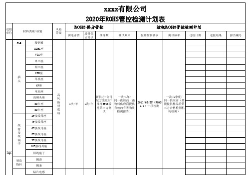
從化市鎧碩塑胶有限公司KAI SUO PLASTYC INDUSTRY CO.,LTD. RoHS管理标准程序文件编号:KS-QE-01编制:审核:批准:生效日期:2014年02月01日修改记录表版本修订次数修订日期修订理由及内容摘要修订人A/0 2014-02-01 初版作成莫智贤A/1 2015-02-01 新增4种邻苯类物质,升级为RoHS 2.0 莫智贤1.0目的1.1定义产品环保管制作业流程及权责,使在对供货商评鉴、样品评估、采购进行检验,制程设计与管制及产品出货等过程得到有效管控,使出货产品危害物含量符合客户要求。
1.2本公司执行有毒物质含量标准:如客户有特别要求者依客户要求执行,无特别要求者依铠硕公司KS-QE-01标准执行。
2.0范围适用于公司所有原材料及直接用于产品加工用之生产辅助材料、半成品、成品环境物质的供货商评鉴、样品评估、采购、进料检验、制程设计与管制及产品出货等环节的环保管制过程。
3.0定义WEEE:废弃电子电器设备指令。
RoHS: 欧盟关于有害物质使用禁令,有害物质含量限制分别为:镉(Cd)为100ppm、铅(Pb)/汞(Hg)/六价铬(Cr6+)/多溴联苯(PBB)/多溴联苯醚(PBDE)五项均为1000ppm,本公司依此建立公司内部标准即为KS-QE-01,以要求所有配合供货商遵守之。
4.0权责4.1 总经理: 负责环境相关物质的管理领导工作,过程重大事项的裁决。
4.2 管理代表: 环境相关物质的管理相关文件的拟定,环境相关物质的法令法规了解及纳入,环境相关物质异常处理及回馈,负责主导公司环境相关物质管理系统之规划、推行、监督、信息沟通及环境相关物质会议的召开,并负责产品环保教育训练的推动。
4.3业务部:接获客户的环保要求及相关规格,并将其传递给工程部(新规格/新产品)或品质管理部。
4.4 技朮部:4.4.1在外购物料承认阶段,评估物料/辅材各项物质成份含量是否符合客户环保规格要求,要求供货商提供相关产品环保证明资料。
1.0目的为确保本公司产品的原材料、成品达到符合ROHS要求,建立一个标准程序实现符合RoHS要求的控制过程。
2.0范围2.1适用于所有需要符合RoHS要求的型号及转换型号来实现符合ROHS要求;2.2适用于ROHS材料引入及未符合RoHS要求的材料更新或者替代;2.3符合ROHS要求的材料与非符合RoHS要求的材料两者需严格区分,有明显的标识;2.4符合RoHS要求的材料控制需在以下位置来控制:2.4.1进料控制,包括所有的原材料成品;2.4.2制程控制,生产的符合RoHS要求的产品制程控制;2.4.3贮藏控制,在仓库贮存或生产所有符合RoHS的原料控制,包括材料、半成品、成品等;2.4.4生产控制;2.4.5成品的包装控制;2.4.6产品的运输控制。
3.0定义3.1RoHS:关于在电子、电气和设备中限制使用某些有害物质的指令4.0符合RoHS要求材料的有关定义、要求和测试方法:4.1RoHS定义:是关于在电子、电气和设备中限制使用某些有害物质的指令。
4.2RoHS含义4.2.1在电子、电气和设备中逐步停止使用RoHS里提到的禁止使用物质;4.2.2WEEE的条文里提出,我们须对人类健康及环境保护意识,减少浪费做出贡献。
4.3RoHS要求与客户要求4.3.1RoHS要求*Cd镉*Pb铅之和<80PPM*Hg汞*Cr6+铬/六价铬*PBB多溴联苯<500PPM*PBDE多溴二苯醚<500PPM4.3.2客户要求4.3.2.1客户有规定的按客户要求执行4.3.2.2未规定的客户对环境管理物质的限定值与欧盟要求一致职责:7.0程序7.1符合RoHS的供应商及材料的管制7.1.1ROHS产品的管制7.1.1.1所有的ROHS材料必须符合RoHS要求,7.1.1.2供应部要确保所有的供应商每年一次递交符合RoHS申明和第三方测试报告。
7.2新物料的RoHS管制程序7.2.1业务部在接到新的定单时应按对客户定单进行评审,评审内容应包括RoHS要求。
1苏州市相城区东桥新千禧彩印厂2苏州市天翔包装有限公司
3苏州市胜达现代包装彩印有限公司4苏州新区印刷厂
5浙江大胜达包装有限公司
6常熟市信诚彩色印刷有限公司
7常熟市双乐彩印包装有限公司
8苏州新区丽达彩印包装有限公司
9无锡市新中彩印厂有限公司
10苏州卓正包装材料有限公司
11苏州宝来印刷包装有限公司
12苏州市金盟包装材料有限公司
13苏州富鑫印刷包装有限公司
14苏州亚力特蜂窝纸制品包装有限公司15苏州万顺彩印有限公司
16苏州市先河印务有限公司
17苏州市元孝装潢印刷有限公司
18苏州市卓越包装印刷有限公司
19太仓市华美彩印有限公司
20深圳市山通电子有限公司
21吴江泰兴电子有限公司
22苏州市金兰德电子有限公司
23苏州长发电器组件厂
24张家港华峰电接插元件有限公司25苏州市诺弗电器有限公司
26适发国际贸易(上海)有限公司
27上海摄月电子电器有限公司
28宁波康伯斯电器有限公司
29昆山周氏电业有限公司
30深圳凯联杨科技有限公司
31江苏常胜电器有限公司
32苏州市宝德电子科技有限公司
33昆山映兴电子有限公司
34朗诗德电气有限公司
35苏州和诚过滤器材有限公司
36浙江朝晖过滤技术股份有限公司37无锡市和泰海绵有限公司
38太仓市金玮电器有限公司
39苏州创佳电子材料有限公司
40苏州市忠诚塑料制品厂
41太仓市永盛塑料制品有限公司
42苏州市相城区蠡口新陆五金厂
43上海孙腾商贸有限公司
44苏州工业园区久泰精密电子有限公司45苏州凯泽精密电子有限公司
46杭州卡丽科技有限公司
47苏州工业园区天恒科技有限公司48桐乡市健民过滤材料有限公司
49苏州万士德净化产品有限公司
50苏州市相城区民康电器配套厂
51苏州市群力过滤器有限公司
52苏州市沧浪区中南净化器材厂53苏州七彩塑胶有限公司
54苏州工业园区朝联塑业有限公司55苏州市集虹新材料科技有限公司56苏州隆诚工程塑料有限公司
57苏州新区枫盛塑料制品厂
58苏州市大元塑业有限公司
59苏州市勤协新型塑料有限公司60苏州俄邦工程塑胶有限公司
61苏州豪仕嘉塑业有限公司
62苏州工业园区和昌电器有限公司63苏州市科创聚合物有限公司
64金华市春光橡塑软管有限公司65巴拉斯塑胶(苏州)有限公司66磐安县景光塑胶制品厂
67苏州富利达工贸有限公司
68太仓华美达塑料电器有限公司69常熟市亚德实业有限公司
70苏州市群艺塑料电器厂
71太仓市惠得利弹簧有限公司
72苏州市胜能弹簧五金制品有限公司73苏州市吴中区龙盛金属制品厂74余姚市汇丰电器有限公司
75天津希日博司塔金属有限公司76苏州市泰顺电器有限公司
77苏州市宏伟电器有限公司
78苏州信德电器有限公司
79苏州昊乐电器有限公司
80苏州爱建电器有限公司
81苏州市欧陆杰电器有限公司
82苏州康元电器有限公司
83上海范立电器有限公司
84克恩-里伯斯(太仓)有限公司85宁波市北仑区大矸前宋五金元件厂86宁波宗大电器发条有限公司
87海门市德胜标准件厂
88海门市厂洪螺丝厂
89靖江市卓越紧固件制造有限公司90常熟市新达紧固件厂
91苏州巨隆金属制品有限公司
92苏州市维达电器配件厂
93苏州新秀五金电器配件厂
94苏州金利达冲压件有限公司
95苏州市华杰橡胶厂
96太仓市祖达橡胶厂
97太仓精艺弹簧有限公司
98苏州欣亚特橡塑制品有限公司99苏州思飞硅橡胶制品有限公司100宁波凯驰胶带有限公司。