LT1937中文资料
- 格式:pdf
- 大小:365.89 KB
- 文档页数:12
5ms/DIV123456GND (Pins 1, 20, Exposed Pad Pin 29): Ground. Tie both GND pins and the exposed pad directly to a local ground plane. The ground metal to the exposed pad should be as wide as possible for better heat dissipation. Multiple vias (to ground plane under the ground backplane) placed close to the exposed pad can further aid in reducing thermal resistance.VC1 (Pin 2): Switching Regulator 1 Error Amplifier Com-pensation. Connect a resistor/capacitor network in series with this pin.VC2 (Pin 3): Error Amplifier Compensation for Switcher2. Connect a resistor/capacitor network in series with this pin.FB1 (Pin 4): Switching Regulator 1 Feedback. Tie the resistor divider tap to this pin and set V LOGIC according to V LOGIC = 1.25 • (1 + R2/R1). Reference designators refer to Figure 1.FB2 (Pin 5): Feedback for Switch 2. Tie the resistor divider tap to this pin and set AV DD according to AV DD = 1.25 •(1 + R6/R5).FB3 (Pin 6): Switching Regulator 3 Feedback. Tie the resistor divider tap to this pin and set V ON according to V ON = 1.25 • (1 + R9/R8) – 150mV.NFB4 (Pin 7): Switching Regulator 4 Negative Feedback. Switcher 4 can be used to generate a positive or negative output. When regulating a negative output, tie the resistor divider tap to this pin. Negative output voltage can be set by the equation V OFF = –1.245 • (R3/R4) with R4 set to 10k. Tie the NFB4 pin to FB4 for positive output voltages. FB4 (Pin 8): Feedback for Switch 4. When generating a positive voltage from switch 4, tie the resistor divider tap to this pin. When generating a negative voltage, tie a 10k resistor between FB4 and NFB4 (R4).VC3 (Pin 9): Switching Regulator 3 Error Amplifier Com-pensation. Connect a resistor/capacitor network in series with this pin.VC4 (Pin 10): Switching Regulator 4 Error Amplifier Compensation. Connect a resistor/capacitor network in series with this pin.SGND (Pin 11): Signal Ground. Return ground trace from the FB resistor networks and V C pin compensation compo-nents directly to this pin and then tie to ground. BOOST (Pin 12): The BOOST pin is used to provide a drive voltage, higher than V IN, to the switch 1 drive circuit. SW1 (Pins 13, 14): The SW1 pins are the emitter of the internal NPN bipolar power transistor for switching regu-lator 1. These pins must be tied together for proper operation. Connect these pins to the inductor, catch diode and boost capacitor.V IN (Pins 15, 16): The V IN pins supply current to the LT1943’s internal regulator and to the internal power transistor for switch 1. These pins must be tied together and locally bypassed.SS-234 (Pin 17): This is the soft-start pin for switching regulators 2, 3 and 4. Place a soft-start capacitor here to limit start-up inrush current and output voltage ramp rate. When the BIAS pin reaches 2.8V, a 1.7µA current source begins charging the capacitor. When the capacitor voltage reaches 0.8V, switches 2, 3 and 4 turn on and begin switching. For slower start-up, use a larger capacitor. When this pin is pulled to ground, switches 2, 3 and 4 are disabled. For complete shutdown, tie RUN-SS to ground. RUN-SS (Pin 18): This is the soft-start pin for switching regulator 1. Place a soft-start capacitor here to limit start-up inrush current and output voltage ramp rate. When power is applied to the V IN pin, a 1.7µA current source charges the capacitor. When the voltage at this pin reaches 0.8V, switch 1 turns on and begins switching. For slower start-up, use a larger capacitor. For complete shutdown, tie RUN-SS to ground.SW4 (Pin 19): This is the collector of the internal NPN bipolar power transistor for switching regulator 4. Mini-mize metal trace area at this pin to keep EMI down.UUUPI FU CTIO S71943faSW3 (Pin 21): This is the collector of the internal NPN bipolar power transistor for switching regulator 3. Mini-mize metal trace area at this pin to keep EMI down. BIAS (Pin 22): The BIAS pin is used to improve efficiency when operating at higher input voltages. Connecting this pin to the output of switching regulator 1 forces most of the internal circuitry to draw its operating current from V LOGIC rather than V IN. The drivers of switches 2, 3 and 4 are supplied by BIAS. Switches 2, 3 and 4 will not switch until the BIAS pin reaches approximately 2.8V. BIAS must be tied to V LOGIC.PGOOD (Pin 23): Power Good Comparator Output. This is the open collector output of the power good comparator and can be used in conjunction with an external P-Channel MOSFET to provide output disconnect for AV DD as shown in the 5V Input, Quad Output TFT-LCD Power Supply on the last page of the data sheet. When switcher 2’s output reaches approximately 90% of its programmed voltage, PGOOD will be pulled to ground. This will pull down on the gate of the MOSFET, connecting AV DD. A 100k pull-up resistor between the source and gate of the P-channel MOSFET keeps it off when switcher 2’s output is low.E3 (Pin 24): This is switching regulator 3’s output and the emitter of the output disconnect PNP. Tie the output capacitor and resistor divider here.C T (Pin 25): Timing Capacitor Pin. This is the input to the V ON timer and programs the time delay from all four feedback pins reaching 1.125V to V ON turning on. The C T capacitor value can be set using the equation C = (20µA •t DELAY)/1.1V.V ON (Pin 26): This is the delayed output for switching regulator 3. V ON reaches its programmed voltage after the internal C T timer times out. Protection circuitry ensures V ON is disabled if any of the four outputs are more than 10% below normal voltage.SW2 (Pins 27, 28): The SW2 pins are the collector of the internal NPN bipolar power transistor for switching regu-lator 2. These pins must be tied together. Minimize trace area at these pins to keep EMI down.UUUPI FU CTIO S81943fa9101943faOPERATIOUFigure 2. LT1943 Power-Up Sequence. (Traces From Both Photos are Synchronized to the Same Trigger)RUN-SS 2V/DIV V LOGIC 5V/DIV I L11A/DIV I L2+L31A/DIV SS-2342V/DIV AV DD 20V/DIV PGOOD 20V/DIV5ms/DIV1943 F03aV OFF 10V/DIV V CT 2V/DIV I L4500mA/DIV I L5500mA/DIVV E320V/DIV V ON 50V/DIV5ms/DIV1943 F03b(2a)(2b)The LT1943 is a highly integrated power supply IC con-taining four separate switching regulators. All four switch-ing regulators have their own oscillator with frequency foldback and use current mode control. Switching regula-tor 1 consists of a step-down regulator with a switch current limit of 2.4A. Switching regulator 2 can be config-ured as a step-up or SEPIC converter and has a 2.6A switch. Switching regulator 3 consists of a step-up regu-lator with a 0.35A switch as well as an integrated Schottky diode. Switching regulator 4 has two feedback pins (FB4and NFB4) and can directly regulate positive or negative output voltages. The four regulators share common cir-cuitry including input source, voltage reference, and mas-ter oscillator. Operation can be best understood by refer-ring to the Block Diagram as shown in Figure 1.If the RUN/SS pin is pulled to ground, the LT1943 is shut down and draws 35µA from the input source tied to V IN . An internal 1.7µA current source charges the external soft-start capacitor, generating a voltage ramp at this pin. If the RUN/SS pin exceeds 0.6V, the internal bias circuits turn on, including the internal regulator, reference, and 1.1MHz master oscillator. The master oscillator generates four clock signals, one for each of the switching regulators.Switching regulator 1 will only begin to operate when the RUN/SS pin reaches 0.8V. Switcher 1 generates V LOGIC ,which must be tied to the BIAS pin. When BIAS reaches 2.8V, the NPN pulling down on the SS-234 pin turns off,allowing an internal 1.7µA current source to charge the external capacitor tied to the SS-234 pin. When the voltage on the SS-234 pin reaches 0.8V, switchers 2, 3 and 4 are enabled. AV DD and V OFF will then begin rising at a ramp rate determined by the capacitor tied to the SS-234 pin.When all the outputs reach 90% of their programmed voltages, the NPN pulling down on the C T pin will turn off,and an internal 20µA current source will charge the exter-nal capacitor tied to the C T pin. When the C T pin reaches 1.1V, the output disconnect PNP turns on, connecting V ON . In the event of any of the four outputs dropping below 10% of their programmed voltage, PanelProtect circuitry pulls the C T pin to GND, disabling V ON .A power good comparator monitors AV DD and turns on when the FB2 pin is at or above 90% of its regulated value.The output is an open collector transistor that is off when the output is out of regulation, allowing an external resis-tor to pull the pin high. This pin can be used with a P-channel MOSFET that functions as an output disconnect for AV DD .The four switchers are current mode regulators. Instead of directly modulating the duty cycle of the power switch, the feedback loop controls the peak current in the switch during each cycle. Compared to voltage mode control,current mode control improves loop dynamics and pro-vides cycle-by-cycle current limit.The control loop for the four switchers is similar. A pulse from the slave oscillator sets the RS latch and turns on the internal NPN bipolar power switch. Current in the switch and the external inductor begins to increase. When this current exceeds a level determined by the voltage at V C, the current comparator resets the latch, turning off the switch. The current in the inductor flows through the Schottky diode and begins to decrease. The cycle begins again at the next pulse from the oscillator. In this way, the voltage on the V C pin controls the current through the inductor to the output. The internal error amplifier regulates the output voltage by continually adjusting the V C pin voltage. The threshold for switching on the V C pin is 0.8V, and an active clamp of 1.8V limits the output current. The RUN/SS and SS-234 pins also clamp the V C pin voltage. As the internal current source charges the external soft-start capacitor, the current limit increases slowly.Each switcher contains an extra, independent oscillator to perform frequency foldback during overload conditions. This slave oscillator is normally synchronized to the mas-ter oscillator. A comparator senses when V FB is less than 0.5V and switches the regulator from the master oscillator to a slower slave oscillator. The V FB pin is less than 0.5V during startup, short-circuit, and overload conditions. Frequency foldback helps limit switch current and power dissipation under these conditions.The switch driver for SW1 operates either from V IN or from the BOOST pin. An external capacitor and diode are used to generate a voltage at the BOOST pin that is higher than the input supply. This allows the driver to saturate the internal bipolar NPN power switch for efficient operation. STEP-DOWN CONSIDERATIONSFB Resistor NetworkThe output voltage for switcher 1 is programmed with a resistor divider (refer to the Block Diagram) between the output and the FB pin. Choose the resistors according to: R2 = R1(V OUT/1.25V – 1)R1 should be 10kΩ or less to avoid bias current errors.Input Voltage RangeThe minimum operating voltage of switcher 1 is deter-mined either by the LT1943’s undervoltage lockout of ~4V, or by its maximum duty cycle. The duty cycle is the fraction of time that the internal switch is on and is determined by the input and output voltages:DC = (V OUT + V F)/(V IN – V SW + V F)where V F is the forward voltage drop of the catch diode (~0.4V) and V SW is the voltage drop of the internal switch (~0.3V at maximum load). This leads to a minimum input voltage ofV IN(MIN) = (V OUT + V F)/DC MAX – V F + V SWwith DC MAX = 0.82.Inductor Selection and Maximum Output CurrentA good first choice for the inductor value is:L = (V OUT + V F)/1.2where V F is the voltage drop of the catch diode (~0.4V) and L is in µH. The inductor’s RMS current rating must be greater than the maximum load current and its saturation current should be at least 30% higher. For highest effi-ciency, the series resistance (DCR) should be less than 0.1Ω. Table 1 lists several vendors and types that are suitable.The optimum inductor for a given application may differ from the one indicated by this simple design guide. A larger value inductor provides a higher maximum load current, and reduces the output voltage ripple. If your load is lower than the maximum load current, then you can relax the value of the inductor and operate with higher ripple current. This allows you to use a physically smaller inductor, or one with a lower D CR resulting in higher efficiency. Be aware that the maximum load current depends on input voltage. A graph in the Typical Perfor-mance section of this data sheet shows the maximum load current as a function of input voltage and inductor value for V OUT = 3.3V. In addition, low inductance may result in discontinuous mode operation, which further reducesOPERATIO111943fa12Output Capacitor SelectionFor 5V and 3.3V outputs, a 10µF 6.3V ceramic capacitor (X5R or X7R) at the output results in very low output voltage ripple and good transient response. Other types and values will also work; the following discussion ex-plores tradeoffs in output ripple and transient perfor-mance.The output capacitor filters the inductor current to gener-ate an output with low voltage ripple. It also stores energy in order satisfy transient loads and stabilizes the LT1943’s control loop. Because the LT1943 operates at a high frequency, minimal output capacitance is necessary. In addition, the control loop operates well with or without the presence of output capacitor series resistance (ESR). Ceramic capacitors, which achieve very low output ripple and small circuit size, are therefore an option.You can estimate output ripple with the following equations:V RIPPLE = ∆I L/(8 • f • C OUT) for ceramic capacitors, and V RIPPLE = ∆I L • ESR for electrolytic capacitors (tantalum and aluminum);where ∆I L is the peak-to-peak ripple current in the induc-tor. The RMS content of this ripple is very low so the RMS current rating of the output capacitor is usually not of concern. It can be estimated with the formula:I C(RMS)= ∆I L/√12Another constraint on the output capacitor is that it must have greater energy storage than the inductor; if the stored energy in the inductor transfers to the output, the resulting voltage step should be small compared to the regulation voltage. For a 5% overshoot, this requirement indicates: C OUT > 10 • L • (I LIM/V OUT)2The low ESR and small size of ceramic capacitors make them the preferred type for LT1943 applications. Not all ceramic capacitors are the same, however. Many of the higher value capacitors use poor dielectrics with high temperature and voltage coefficients. In particular, Y5V and Z5U types lose a large fraction of their capacitance with applied voltage and at temperature extremes.Because loop stability and transient response depend on the value of C OUT, this loss may be unacceptable. Use X7R and X5R types.Electrolytic capacitors are also an option. The ESRs of most aluminum electrolytic capacitors are too large to deliver low output ripple. Tantalum and newer, lower ESR organic electrolytic capacitors intended for power supply use are suitable, and the manufacturers will specify the ESR. Chose a capacitor with a low enough ESR for the required output ripple. Because the volume of the capaci-tor determines its ESR, both the size and the value will be larger than a ceramic capacitor that would give similar ripple performance. One benefit is that the larger capaci-tance may give better transient response for large changes in load current. Table 2 lists several capacitor vendors. Table 2. Low ESR Surface Mount CapacitorsVendor Type SeriesTaiyo Yuden Ceramic X5R, X7RAVX Ceramic X5R, X7RTantalum TPSKemet Tantalum T491, T494, T495Ta Organic T520Al Organic A700Sanyo Ta or Al Organic POSCAP Panasonic Al Organic SP CAPTDK Ceramic X5R, X7RDiode SelectionThe catch diode (D1 from Figure 1) conducts current only during switch off time. Average forward current in normal operation can be calculated from:I D(AVG) = I OUT (V IN – V OUT)/V INThe only reason to consider a diode with a larger current rating than necessary for nominal operation is for the worst-case condition of shorted output. The diode current will then increase to the typical peak switch current. Peak reverse voltage is equal to the regulator input volt-age. Use a diode with a reverse voltage rating greater than the input voltage. Table 3 lists several Schottky diodes and their manufacturers.OPERATIO131943fa1415161943famust have low impedance at the switching frequency to do this effectively and it must have an adequate ripple current rating. The input capacitor RMS current can be calculated from the step-down output voltage and current, and the input voltage:C I V V V V I INRMS OUT OUT IN UT INOUT=<•(–)02and is largest when V IN = 2 V OUT (50% duty cycle). The ripple current contribution from the other channels will be minimal. Considering that the maximum load current from switcher 1 is ~2.8A, RMS ripple current will always be less than 1.4A.The high frequency of the LT1943 reduces the energy storage requirements of the input capacitor, so that the capacitance required is less than 10µF. The combination of small size and low impedance (low equivalent series resistance or ESR) of ceramic capacitors makes them the preferred choice. The low ESR results in very low voltage ripple. Ceramic capacitors can handle larger magnitudes of ripple current than other capacitor types of the same value. Use X5R and X7R types.An alternative to a high value ceramic capacitor is a lower value along with a larger electrolytic capacitor, for ex-ample a 1µF ceramic capacitor in parallel with a low ESR tantalum capacitor. For the electrolytic capacitor, a value larger than 10µF will be required to meet the ESR and ripple current requirements. Because the input capacitor is likely to see high surge currents when the input source is applied, only consider a tantalum capacitor if it has the appropriate surge current rating. The manufacturer may also recommend operation below the rated voltage of the capacitor. Be sure to place the 1µF ceramic as close as possible to the V IN and GND pins on the IC for optimal noise immunity.A final caution is in order regarding the use of ceramic capacitors at the input. A ceramic input capacitor can combine with stray inductance to form a resonant tank circuit. If power is applied quickly (for example by plug-ging the circuit into a live power source), this tank can ring,doubling the input voltage and damaging the LT1943. Thesolution is to either clamp the input voltage or dampen thetank circuit by adding a lossy capacitor (an electrolytic) in parallel with the ceramic capacitor. For details, see Appli-cation Note 88.Soft-Start and ShutdownThe RUN/SS (Run/Soft-Start) pin is used to place the switching regulators and the internal bias circuits in shut-down mode. It also provides a soft-start function, along with SS-234. If the RUN/SS is pulled to ground, the LT1943 enters its shutdown mode with all regulators off and quiescent current reduced to ~35µA. An internal 1.7µA current source pulls up on the RUN/SS and SS-234pins. If the RUN/SS pin reaches ~0.8V, the internal bias circuits start and the quiescent currents increase to their nominal levels.If a capacitor is tied from the RUN/SS or SS-234 pins to ground, then the internal pull-up current will generate a voltage ramp on these pins. This voltage clamps the V C pin, limiting the peak switch current and therefore input current during start-up. The RUN/SS pin clamps V C1, and the SS-234 pin clamps the V C2, V C3, and V C4 pins. A good value for the soft-start capacitors is C OUT /10,000, where C OUT is the value of the largest output capacitor.To shut down SW2, SW3, and SW4, pull the SS-234 pin to ground with an open drain or collector.If the shutdown and soft-start features are not used, leave the RUN/SS and SS-234 pins floating.V ON Pin ConsiderationsThe V ON pin is the delayed output for switching regulator 3. When the C T pin reaches 1.1V, the output disconnect PNP turns on, connecting V ON to E3. The V ON pin is current limited, and will protect the LT1943 and input source from a shorted output. However, if the V ON pin is charged to a high output voltage, and then shorted to ground through a long wire, unpredictable results can occur. The resonant tank circuit created by the inductance of the long wire and the capacitance at the V ON pin can ring the V ON pin several volts below ground. This can lead to large and potentially damaging currents internal to the LT1943. If the V ON output may be shorted after being fully charged, thereOPERATIO17Figure 5. Top Side PCB Layout 1943 F05GNDV INAV DDV OFFGNDV LOGIC1819Information furnished by Linear Technology Corporation is believed to be accurate and reliable.However, no responsibility is assumed for its use. Linear Technology Corporation makes no represen-tation that the interconnection of its circuits as described herein will not infringe on existing patent rights.20Linear Technology Corporation1630 McCarthy Blvd., Milpitas, CA 95035-7417(408) 432-1900 ● FAX: (408) 434-0507 ● © LINEAR TECHNOLOGY CORPORA TION 2003LT/LT 0405 REV A • PRINTED IN USA。
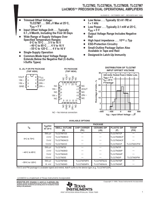
元器件交易网IMPORTANT NOTICETexas Instruments and its subsidiaries (TI) reserve the right to make changes to their products or to discontinueany product or service without notice, and advise customers to obtain the latest version of relevant informationto verify, before placing orders, that information being relied on is current and complete. All products are soldsubject to the terms and conditions of sale supplied at the time of order acknowledgement, including thosepertaining to warranty, patent infringement, and limitation of liability.TI warrants performance of its semiconductor products to the specifications applicable at the time of sale inaccordance with TI’s standard warranty. Testing and other quality control techniques are utilized to the extentTI deems necessary to support this warranty. Specific testing of all parameters of each device is not necessarilyperformed, except those mandated by government requirements.CERTAIN APPLICATIONS USING SEMICONDUCTOR PRODUCTS MAY INVOLVE POTENTIAL RISKS OFDEATH, PERSONAL INJURY, OR SEVERE PROPERTY OR ENVIRONMENTAL DAMAGE (“CRITICALAPPLICATIONS”). TI SEMICONDUCTOR PRODUCTS ARE NOT DESIGNED, AUTHORIZED, ORWARRANTED TO BE SUITABLE FOR USE IN LIFE-SUPPORT DEVICES OR SYSTEMS OR OTHERCRITICAL APPLICATIONS. INCLUSION OF TI PRODUCTS IN SUCH APPLICATIONS IS UNDERSTOOD TOBE FULLY AT THE CUSTOMER’S RISK.In order to minimize risks associated with the customer’s applications, adequate design and operatingsafeguards must be provided by the customer to minimize inherent or procedural hazards.TI assumes no liability for applications assistance or customer product design. TI does not warrant or representthat any license, either express or implied, is granted under any patent right, copyright, mask work right, or otherintellectual property right of TI covering or relating to any combination, machine, or process in which suchsemiconductor products or services might be or are used. TI’s publication of information regarding any thirdparty’s products or services does not constitute TI’s approval, warranty or endorsement thereof.Copyright © 1999, Texas Instruments Incorporated。

PSM Step-up DC/DC ConverterFeatures1~4 Cell Alkaline Battery Operating Range Output Voltage Range: 2.5V~5.0V in 0.1V In-crementsMinimum External Component (L, D, C)100KHz Max. Oscillation Frequency75% Duty RatioUp to 80% Efficiency±2% High Output Voltage Accuracy< 100ppm/°C Temperature CoefficientSOT-89 and SOT-23-5 Small Packages ApplicationsPower Source for Portable EquipmentsHandheld Computers, PalmtopsDigital Still Cameras, CamcordersCellular Phones, PagersPortable Multimedia Players General DescriptionThe G5130/G5131 boost converter is designed for use of main power source on portable equipments.It consist of an oscillator, PSM control logic circuit, an embedded power MOS (LX switch), accurate voltage reference, error amplifier, feedback resistors, and LX protection circuit.Only 3 external components (includes 1 inductor, 1 diode and 1 capacitor) are needed to construct the power application.For larger output power application, G5131 can be used to drive an external NPN device for more input current.Pin Configuration Typical Application Circuit2.5V~5.0V2.5V~5.0VStep 0.1VStep 0.1VOrdering InformationORDER NUMBER ORDER NUMBER(Pb free)MARKINGOUTPUTVOLTAGE (V)TEMP.RANGEPACKAGEG5130-30T11U G5130-30T11Uf EA30x 3.0 -40°C ~ +85°C SOT-23-5G5130-33T11U G5130-33T11Uf EA33x 3.3 -40°C ~ +85°C SOT-23-5G5130-42T11U G5130-42T11Uf EA42x 4.2 -40°C ~ +85°C SOT-23-5G5130-50T11U G5130-50T11Uf EA50x 5.0 -40°C ~ +85°C SOT-23-5G5130-30T21U G5130-30T21Uf 5130Fx 3.0 -40°C ~ +85°C SOT-89G5130-33T21U G5130-33T21Uf 5130Ix 3.3 -40°C ~ +85°C SOT-89G5130-42T21U G5130-42T21Uf 5130Rx 4.2 -40°C ~ +85°C SOT-89G5130-50T21U G5130-50T21Uf 5130Zx 5.0 -40°C ~ +85°C SOT-89G5131-30T11U G5131-30T11Uf EB30x 3.0 -40°C ~ +85°C SOT-23-5G5131-33T11U G5131-33T11Uf EB33x 3.3 -40°C ~ +85°C SOT-23-5G5131-42T11U G5131-42T11Uf EB42x 4.2 -40°C ~ +85°C SOT-23-5G5131-50T11U G5131-50T11Uf EB50x 5.0 -40°C ~ +85°C SOT-23-5G5131-30T21U G5131-30T21Uf 5131Fx 3.0 -40°C ~ +85°C SOT-89G5131-33T21U G5131-33T21Uf 5131Ix 3.3 -40°C ~ +85°C SOT-89G5131-42T21U G5131-42T21Uf 5131Rx 4.2 -40°C ~ +85°C SOT-89G5131-50T21U G5131-50T21Uf 5131Zx 5.0 -40°C ~ +85°C SOT-89For other output voltage, please contact us at sales@Order Number IdentificationGXXXX XX XXTypePin OptionTypeVoltage OptionPart NumberG5130: Internal MOS (LX)G5131: External MOS (EXT)PACKAGE TYPE PIN OPTION PACKINGT1 : SOT-23-5 SOT89 SOT23-5U & D: Tape & Reel Direction T2 : SOT-89 1 2 3 1 2 3 4 5G5130 1:GND VOUT LX 1:CE VOUT NC GND LXG5131 1:GND VOUT EXT 1:CE VOUT NC GND EXTORDER NUMBER ORDER NUMBER(Pb free)OUTPUTVOLTAGE (V)MARKINGG5130-25T11U G5130-25T11Uf 2.5 EA25x G5130-26T11U G5130-26T11Uf 2.6 EA26x G5130-27T11U G5130-27T11Uf 2.7 EA27x G5130-28T11U G5130-28T11Uf 2.8 EA28x G5130-29T11U G5130-29T11Uf 2.9 EA29x G5130-30T11U G5130-30T11Uf 3.0 EA30x G5130-31T11U G5130-31T11Uf 3.1 EA31x G5130-32T11U G5130-32T11Uf 3.2 EA32x G5130-33T11U G5130-33T11Uf 3.3 EA33x G5130-34T11U G5130-34T11Uf 3.4 EA34x G5130-35T11U G5130-35T11Uf 3.5 EA35x G5130-36T11U G5130-36T11Uf 3.6 EA36x G5130-37T11U G5130-37T11Uf 3.7 EA37x G5130-38T11U G5130-38T11Uf 3.8 EA38x G5130-39T11U G5130-39T11Uf 3.9 EA39x G5130-40T11U G5130-40T11Uf 4.0 EA40x G5130-41T11U G5130-41T11Uf 4.1 EA41x G5130-42T11U G5130-42T11Uf 4.2 EA42x G5130-43T11U G5130-43T11Uf 4.3 EA43x G5130-44T11U G5130-44T11Uf 4.4 EA44x G5130-45T11U G5130-45T11Uf 4.5 EA45x G5130-46T11U G5130-46T11Uf 4.6 EA46x G5130-47T11U G5130-47T11Uf 4.7 EA47x G5130-48T11U G5130-48T11Uf 4.8 EA48x G5130-49T11U G5130-49T11Uf 4.9 EA49x G5130-50T11U G5130-50T11Uf 5.0 EA50x Note: T1: SOT-23-5Selector GuideORDER NUMBER ORDER NUMBER(Pb free)OUTPUTVOLTAGE (V)MARKINGG5130-25T21U G5130-25T21Uf 2.5 5130Ax G5130-26T21U G5130-26T21Uf 2.6 5130Bx G5130-27T21U G5130-27T21Uf 2.7 5130Cx G5130-28T21U G5130-28T21Uf 2.8 5130Dx G5130-29T21U G5130-29T21Uf 2.9 5130Ex G5130-30T21U G5130-30T21Uf 3.0 5130Fx G5130-31T21U G5130-31T21Uf 3.1 5130Gx G5130-32T21U G5130-32T21Uf 3.2 5130Hx G5130-33T21U G5130-33T21Uf 3.3 5130Ix G5130-34T21U G5130-34T21Uf 3.4 5130Jx G5130-35T21U G5130-35T21Uf 3.5 5130Kx G5130-36T21U G5130-36T21Uf 3.6 5130Lx G5130-37T21U G5130-37T21Uf 3.7 5130Mx G5130-38T21U G5130-38T21Uf 3.8 5130Nx G5130-39T21U G5130-39T21Uf 3.9 5130Ox G5130-40T21U G5130-40T21Uf 4.0 5130Px G5130-41T21U G5130-41T21Uf 4.1 5130Qx G5130-42T21U G5130-42T21Uf 4.2 5130Rx G5130-43T21U G5130-43T21Uf 4.3 5130Sx G5130-44T21U G5130-44T21Uf 4.4 5130Tx G5130-45T21U G5130-45T21Uf 4.5 5130Ux G5130-46T21U G5130-46T21Uf 4.6 5130Vx G5130-47T21U G5130-47T21Uf 4.7 5130Wx G5130-48T21U G5130-48T21Uf 4.8 5130Xx G5130-49T21U G5130-49T21Uf 4.9 5130Yx G5130-50T21U G5130-50T21Uf 5.0 5130Zx Note: T2: SOT-89ORDER NUMBER ORDER NUMBER(Pb free)OUTPUTVOLTAGE (V)MARKINGG5131-25T11U G5131-25T11Uf 2.5 EB25x G5131-26T11U G5131-26T11Uf 2.6 EB26x G5131-27T11U G5131-27T11Uf 2.7 EB27x G5131-28T11U G5131-28T11Uf 2.8 EB28x G5131-29T11U G5131-29T11Uf 2.9 EB29x G5131-30T11U G5131-30T11Uf 3.0 EB30x G5131-31T11U G5131-31T11Uf 3.1 EB31x G5131-32T11U G5131-32T11Uf 3.2 EB32x G5131-33T11U G5131-33T11Uf 3.3 EB33x G5131-34T11U G5131-34T11Uf 3.4 EB34x G5131-35T11U G5131-35T11Uf 3.5 EB35x G5131-36T11U G5131-36T11Uf 3.6 EB36x G5131-37T11U G5131-37T11Uf 3.7 EB37x G5131-38T11U G5131-38T11Uf 3.8 EB38x G5131-39T11U G5131-39T11Uf 3.9 EB39x G5131-40T11U G5131-40T11Uf 4.0 EB40x G5131-41T11U G5131-41T11Uf 4.1 EB41x G5131-42T11U G5131-42T11Uf 4.2 EB42x G5131-43T11U G5131-43T11Uf 4.3 EB43x G5131-44T11U G5131-44T11Uf 4.4 EB44x G5131-45T11U G5131-45T11Uf 4.5 EB45x G5131-46T11U G5131-46T11Uf 4.6 EB46x G5131-47T11U G5131-47T11Uf 4.7 EB47x G5131-48T11U G5131-48T11Uf 4.8 EB48x G5131-49T11U G5131-49T11Uf 4.9 EB49x G5131-50T11U G5131-50T11Uf 5.0 EB50x Note: T1: SOT-23-5Selector GuideORDER NUMBER ORDER NUMBER(Pb free)OUTPUTVOLTAGE (V)MARKINGG5131-25T21U G5131-25T21Uf 2.5 5131Ax G5131-26T21U G5131-26T21Uf 2.6 5131Bx G5131-27T21U G5131-27T21Uf 2.7 5131Cx G5131-28T21U G5131-28T21Uf 2.8 5131Dx G5131-29T21U G5131-29T21Uf 2.9 5131Ex G5131-30T21U G5131-30T21Uf 3.0 5131Fx G5131-31T21U G5131-31T21Uf 3.1 5131Gx G5131-32T21U G5131-32T21Uf 3.2 5131Hx G5131-33T21U G5131-33T21Uf 3.3 5131Ix G5131-34T21U G5131-34T21Uf 3.4 5131Jx G5131-35T21U G5131-35T21Uf 3.5 5131Kx G5131-36T21U G5131-36T21Uf 3.6 5131Lx G5131-37T21U G5131-37T21Uf 3.7 5131Mx G5131-38T21U G5131-38T21Uf 3.8 5131Nx G5131-39T21U G5131-39T21Uf 3.9 5131Ox G5131-40T21U G5131-40T21Uf 4.0 5131Px G5131-41T21U G5131-41T21Uf 4.1 5131Qx G5131-42T21U G5131-42T21Uf 4.2 5131Rx G5131-43T21U G5131-43T21Uf 4.3 5131Sx G5131-44T21U G5131-44T21Uf 4.4 5131Tx G5131-45T21U G5131-45T21Uf 4.5 5131Ux G5131-46T21U G5131-46T21Uf 4.6 5131Vx G5131-47T21U G5131-47T21Uf 4.7 5131Wx G5131-48T21U G5131-48T21Uf 4.8 5131Xx G5131-49T21U G5131-49T21Uf 4.9 5131Yx G5131-50T21U G5131-50T21Uf 5.0 5131Zx Note: T2: SOT-89Absolute Maximum RatingsLX to GND…………….…..……………..…-0.3V to +7V CE to GND….……………..………..……...-0.3V to +7V VOUT to GND.…….…..................……….-0.3V to +7V Operating Temperature Range (Note 1)..-40°C to +85°CJunction Temperature ......…......…......……........+125°C Storage Temperature…………........…..-65°C to +150°C Reflow Temperature (soldering, 10 sec)…..…....+260°CStress beyond those listed under “Absolute Maximum Rating” may cause permanent damage to the device.Electrical Characteristics(V OUT = 3.3V, V IN = 1.8V, T A = 25°C )PARAMETER CONDITION MIN TYP MAX UNITOutput Voltage Accuracy-2 --- +2 % Input Voltage Range ------6.5VStart-up Voltage --- 0.9 ---VHold-on Voltage--- 0.5 --- VNo Switching (I DD2) --- 10 15 µASwitching (I DD1) --- 20 --- µAInput CurrentNo Load (I IN ) ---30 --- µA LX Switch On ResistanceV LX = 0.4V --- 2 6Ω LX Leakage Current V LX = 6.0V --- --- 0.1 µAMaximum Oscillation Frequency 70 100 130 KHzDuty Cycle65 75 85 %V LX Voltage Limit--- 1 --- V Efficiency--- 80 --- %Note 1: The G5130 are guaranteed to meet performance specifications from 0°C to 85°C. Specifications over the -40°C to 85°Coperating temperature range are assured by design, characterization and correlation with statistical process controls.Block DiagramCELX VOUTTypical Performance Characteristics(V IN= +3.0V, L=100µH, T A=25°C, unless otherwise noted.)Line Transient Load TransientRecommended Minimum FootprintSOT-89SOT-23-5Power On ResponsePackage InformationSOT-23-5 (T1) PackageNote:1. Package body sizes exclude mold flash protrusions or gate burrs2. Tolerance ±0.1000 mm (4mil) unless otherwise specified3. Coplanarity: 0.1000mm4. Dimension L is measured in gage planeDIMENSIONS IN MILLIMETERSYMBOLMIN NOM MAXA 1.00 1.10 1.30A1 0.00 ----- 0.10A2 0.70 0.80 0.90 b 0.35 0.40 0.50C 0.10 0.15 0.25D 2.70 2.90 3.10E 1.40 1.60 1.80e ----- 1.90(TYP) ----- e1 ----- 0.95 ----- H 2.60 2.80 3.00L 0.37 ------ ----- θ1 1º 5º9ºSOT-89 (T2) PackageDIMENSIONS IN MILLIMETER DIMENSIONS IN INCH SYMBOLMIN NOM MAX MIN NOM MAXA 1.40 1.50 1.60 0.055 0.059 0.063 A1 0.80 1.04 ----- 0.031 0.041 ----- b 0.36 0.42 0.48 0.014 0.016 0.018 b1 0.41 0.47 0.53 0.016 0.018 0.020 C 038 0.40 0.43 0.014 0.015 0.017 D 4.404.50 4.600.173 0.177 0.181 D1 1.40 1.60 1.75 0.055 0.062 0.069 HE ----- ----- 4.25 ----- ----- 0.167 E 2.40 2.50 2.60 0.094 0.098 0.102 e 2.90 3.00 3.10 0.114 0.118 0.122Taping SpecificationPACKAGE Q’TY/REELSOT-23-5 3,000 ea SOT-89 1,000 eaGMT Inc. does not assume any responsibility for use of any circuitry described, no circuit patent licenses are implied and GMT Inc. reserves the right at any time without notice to change said circuitry and specifications.SOT-89 Package OrientationSOT-23-5 Package Orientation。