12.03.28东软芯片兼容性说明
- 格式:pdf
- 大小:98.94 KB
- 文档页数:1
数据手册☐产品简介☑数据手册☐产品规格上海东软载波微电子有限公司2018年11月20日产品订购信息地址:中国上海市龙漕路299号天华信息科技园2A楼5层邮编:200235E-mail:******************电话:+86-21-60910333传真:+86-21-60914991网址:版权所有©上海东软载波微电子有限公司本资料内容为上海东软载波微电子有限公司在现有数据资料基础上慎重且力求准确无误编制而成,本资料中所记载的实例以正确的使用方法和标准操作为前提,使用方在应用该等实例时请充分考虑外部诸条件,上海东软载波微电子有限公司不担保或确认该等实例在使用方的适用性、适当性或完整性,上海东软载波微电子有限公司亦不对使用方因使用本资料所有内容而可能或已经带来的风险或后果承担任何法律责任。
基于使本资料的内容更加完善等原因,上海东软载波微电子有限公司保留未经预告的修改权。
使用方如需获得最新的产品信息,请随时用上述联系方式与上海东软载波微电子有限公司联系。
修订历史目录内容目录第1章芯片简介 (3)1. 1芯片概述 (3)1. 2应用领域 (4)1. 3结构框图 (4)1. 4管脚说明(QFN20) (5)1. 5管脚说明(SOP14) (6)第2章芯片工作模式控制 (7)2. 1POWER DOWN模式 (7)2. 2SLEEP模式 (7)2. 3IDLE模式 (8)2. 4TX模式 (8)2. 5RX模式 (8)第3章包结构 (9)3. 1PTX发送数据包结构 (9)3. 2PRX发送ACK包结构 (10)第4章芯片链路控制方式 (11)4. 1硬件链路控制方式 (11)4. 2软件链路控制方式 (11)第5章多PIPE逻辑通道 (12)第6章自动响应ACK与自动重传ART (13)6. 1ACK不带ACK PAYLOAD (13)6. 2ACK带ACK PAYLOAD (13)第7章数据与控制接口 (14)7. 1FIFO (14)7. 2中断 (15)7. 2. 1硬件链路控制中断 (15)7. 2. 2软件链路控制中断 (19)7. 3SPI通信接口 (19)7. 3. 1SPI帧格式 (19)7. 3. 2寄存器访问时序 (20)7. 3. 3FIFO访问时序 (20)7. 3. 4SPI时序参数 (21)第8章其它功能与设置 (22)8. 1芯片复位 (22)8. 2频点设置 (22)8. 3自动频偏校正(AFC) (22)8. 4软件频偏校正 (22)8. 5前导码指示 (22)8. 6RSSI功能 (23)8. 7载波检测指示(Carrier Detect)功能 (23)8. 8FEC、CRC、SCRAMBLE功能 (23)8. 9定长功能 (24)8. 10PAD上拉、滤波、大电流驱动功能 (24)第9章寄存器 (25)9. 1寄存器列表 (25)9. 2寄存器说明 (26)第10章封装信息 (40)10. 1SOP14封装 (40)10. 2QFN20封装 (41)第11章参考设计 (42)11. 1参考设计(SOP14) (42)11. 1. 1参考设计图(SOP14) (42)11. 1. 2设计注意事项(SOP14) (43)11. 2参考设计(QFN20) (44)11. 2. 1参考设计图(QFN20) (44)11. 2. 2设计注意事项(QFN20) (45)第12章电气特性 (46)第13章术语解释 (48)图1-1 QFN20封装示意图 (5)图1-2 SOP14封装示意图 (6)图2-1 工作模式控制示意图 (7)图3-1 PTX发送数据包结构示意图 (9)图3-2 PRX发送ACK包结构示意图 (10)图5-1 4路PIPE通讯示意图 (12)图7-1 FIFO控制示意图 (14)图7-2 ACK不使能情况中断示意图 (15)图7-3 ACK使能不带ACK PAYLOAD中断示意图 (15)图7-4 PTX自动重传情况1中断示意图 (16)图7-5 PTX自动重传情况2中断示意图 (16)图7-6 PTX自动重传情况3中断示意图(重发超时,重发次数为2) (17)图7-7 PRX自动重收中断示意图 (17)图7-8 ACK带ACK PAYLOAD情况中断示意图 (18)图7-9 PTX接收ACK CRC ERROR情况中断示意图 (18)图7-10 PRX无满足条件ACK PAYLOAD发送情况中断示意图 (18)图7-11 软件链路控制方式下中断示意图 (19)图7-12 SPI帧格式 (19)图7-13 SPI写寄存器时序 (20)图7-14 SPI读寄存器时序 (20)图7-15 SPI写FIFO时序 (20)图7-16 SPI读FIFO时序 (20)图7-17 SPI时序参数示意图 (21)图8-1 数据扰码生成器 (24)图10-1 SOP14封装信息 (40)图10-2 QFN20封装信息 (41)图11-1 参考设计SCH(SOP14) (42)图11-2 参考设计PCB(SOP14) (42)图11-3 参考设计SCH(QFN20) (44)图11-4 参考设计PCB(QFN20) (44)表1-1 QFN20封装引脚说明 (5)表1-2 SOP14封装引脚说明 (6)表7-1 SPI时序参数 (21)表9-1 寄存器列表 (25)表9-2 PKTCTRL寄存器说明 (26)表9-3 TRCTL寄存器说明 (26)表9-4 CHANNR寄存器说明 (27)表9-5 MISC0寄存器说明 (27)表9-6 FOCCFG寄存器说明 (27)表9-7 FREQBASE寄存器说明 (28)表9-8 DS_PE寄存器说明 (28)表9-9 THRES寄存器说明 (29)表9-10 MISC1寄存器说明 (29)表9-11 MISC2寄存器说明 (29)表9-12 CDTH寄存器说明 (30)表9-13 RSSI寄存器说明 (30)表9-14 STATUS0寄存器说明 (30)表9-15 STATUS1寄存器说明 (30)表9-16 FIX_LEN_EN寄存器说明 (30)表9-17 FIFO0DATA寄存器说明 (31)表9-18 FIFO1DATA寄存器说明 (31)表9-19 ACKFIFO0DATA寄存器说明 (31)表9-20 ACKFIFO1DATA寄存器说明 (31)表9-21 FIFO0CTRL寄存器说明 (32)表9-22 FIFO1CTRL寄存器说明 (33)表9-23 ACKFIFO0CTRL寄存器说明 (34)表9-24 ACKFIFO1CTRL寄存器说明 (35)表9-25 FIFOSTATUS寄存器说明 (35)表9-26 CLEAR寄存器说明 (35)表9-27 PIPECTRL寄存器说明 (36)表9-28 INT寄存器说明 (38)表9-29 P0ADDR0寄存器说明 (38)表9-30 P0ADDR1寄存器说明 (38)表9-31 P0ADDR2寄存器说明 (38)表9-32 P1ADDR0寄存器说明 (38)表9-33 P1ADDR1寄存器说明 (39)表9-34 P1ADDR2寄存器说明 (39)表9-35 P2ADDR寄存器说明 (39)表9-36 P3ADDR寄存器说明 (39)表9-37 芯片操作条件 (46)表9-38 芯片功耗 (46)表9-39 RF通讯基本参数 (46)表9-40 RF发射机参数 (47)表9-41 RF接收机参数 (47)表9-42 振荡器参数 (47)表9-43 IO端口DC参数 (47)表9-44 芯片状态切换时间参数 (47)表9-45 术语解释 (48)第1章芯片简介1. 1 芯片概述HW2000B是一款低功耗低成本 2.4GHz ISM频段射频收发器芯片,支持频段范围为2402~2483MHz。

芯片描述GC8123是一款低压5V全桥驱动芯片,为摄像机、消费类产品、玩具和其他低压或者电池供电的运动控制类应用提供了集成的电机驱动解决方案。
GC8123能提供高达1.2A的持续输出电流。
可以工作在1.2~7V的电源电压上。
GC8123具有PWM(IN/IN)输入接口,与行业标准器件兼容,并具有过温保护功能。
芯片应用●摄像机●数字单镜头反光(DSLR)镜头●玩具●机器人技术●共享单车锁●水表开关●医疗设备芯片特点●H桥电机驱动器--电源电压1.2~7V--低导通阻抗(HS+LS)420mΩ● 1.2A持续驱动输出电流●PWM(INA/INB)输入模式●内置过温保护●低电流睡眠模式(nA级,INA=INB=0)产品名封装细节描述GC8123SOT23-6 2.92*1.6,e=1.27管脚分布图管脚描述管脚号管脚名称I/O管脚描述SOT23-61OUTB O输出B2GND gnd地3INA I逻辑输入A4OUTA O输出A5VCC power电源6INB I逻辑输入B内部框图图1GC8123内部框图极限参数(一般无其他特殊注明时,T=25℃)参数符号参数范围单位工作电压VCC-0.3~7V 控制输入电压范围INx-0.5~7V 驱动持续电流Irms 1.2A 驱动峰值电流Imax 2.0A工作温度Top-40~100℃结温Tjmax-40~150℃存储温度Tstg-60~150℃静电保护(人体模式)ESD±4000V电气参数(一般无其他特殊注明时,T=25℃,VCC=5V )推荐工作环境:(无其他说明,T=25℃)电气特性:(无其他说明,T=25℃,VCC=5V )参数符号测试条件最小值典型值最大值单位逻辑电源VCC 1.27V 持续输出电流I OUT 0 1.2A 外部PWM 频率f PWM 0250kHZ 逻辑输入电压V logic 07V 工作温度T a-40100℃参数符号测试条件最小值典型值最大值单位VCC 工作电压VCC 357V VCC 工作电流1I VCC VCC=5V ,无PWM 200550uA VCC 工作电流2I VCCQVCC=5V ,INA=INB=0省电模式0.011uA输出H 桥参数上臂+下臂桥导通电阻R dsON VCC=5V ,I o =400mA;420600mΩ关断态漏电流I OFFV out =0V-200200nA逻辑输入脚(INA,INB)逻辑低输入电压V IL高电平到低电平VCC=3V00.75VVCC=5V 0 1.0逻辑高输入电压V IH低电平到高电平VCC=3V1.3VCC VVCC=5V 2.1VCC输入逻辑迟滞V HY VCC=3V 0.5VVCC=6V0.9逻辑低输入电流I IL V in =0-55uA 逻辑高输入电流I IH V in =3.3V50uA 下拉电阻R pd 100kΩ过温保护电路过温保护TSD 150170180℃过温保护迟滞ΔTSD30℃时序参数与曲线TA=25°C,VCC=5V,RL=20Ω参数条件范围单位最小最大T1启动时间300ns T2关断时间220ns T3输入高到输出高延迟100ns T4输入低到输出低延迟100ns T5输出上升沿10188ns T6输出下降沿10188ns图2GC8123输入输出时间参数1图3GC8123输入输出时间参数2功能描述桥臂控制GC8123由PWM输入接口控制,也被称作IN/IN输入模式,其控制真值表如下:INA INB OUTA OUTB功能00Z Z待机休眠态01L H反向10H L正向11L L刹车输出驱动由于输出驱动管的驱动电压Vgs与电源相关,GC8123的H桥输出导通电阻随电压的升高而变小,所以在低压时,芯片的电流能力会有所下降。
HK32AUTO39A-3ACET3数据手册版本:1.0发布日期:2023-08-23深圳市航顺芯片技术研发有限公司前言前言编写目的本文档介绍了HK32AUTO39A-3ACET3系列芯片的功能框图、存储器映射、外设接口、电气特性、管脚封装等,旨在帮助用户快速了解该系列芯片的特点及功能。
读者对象本文适用于以下读者:•开发工程师•芯片测试工程师•芯片选型工程师版本说明本文档对应的产品系列为HK32AUTO39A-3ACET3系列芯片。
修订记录目录1 简介 (1)2 产品概述 (2)2.1 产品特性 (2)2.2 器件一览表 (4)3 功能介绍 (5)3.1 结构框图 (5)3.2 存储器映射 (6)3.3 Flash (6)3.4 SRAM (7)3.5 CRC单元 (7)3.6 NVIC (7)3.7 EXTI (9)3.8 复位 (9)3.8.1 系统复位 (9)3.8.2 电源复位 (9)3.8.3 备份域复位 (10)3.9 时钟 (10)3.9.1 时钟源 (10)3.9.2 时钟树 (10)3.10 Boot模式 (11)3.11 供电方案 (11)3.12 可编程电压监测器(PVD) (12)3.13 低功耗模式 (12)3.14 DMA (12)3.15 RTC和BKP (12)3.15.1 RTC (12)3.15.2 BKP (12)3.16 独立看门狗 (13)3.17 窗口看门狗 (13)3.18 System Tick定时器 (13)3.19 定时器 (13)3.19.1 通用定时器 (13)3.19.2 高级定时器 (13)3.20 I2C总线 (14)3.21 USART (14)3.22 SPI (14)3.23 CAN (14)3.24 USB (14)3.25 GPIO (14)3.26 ADC (14)3.27 温度传感器 (15)3.28 调试及跟踪接口 (15)4 电气性能指标 (16)4.1 最大绝对额定值 (16)4.1.1 极限电压特性 (16)4.1.2 极限电流特性 (16)4.1.3 极限温度特性 (16)4.2 工作参数 (16)4.2.1 推荐工作条件 (16)4.2.2 低压检测 (17)4.2.3 上/下电复位特性 (17)4.2.4 内部参考电压 (18)4.2.5 工作电流特性 (18)4.2.6 HSE时钟特性 (19)4.2.7 LSE时钟特性 (19)4.2.8 HSI时钟特性 (20)4.2.9 LSI时钟特性 (21)4.2.10 PLL特性 (21)4.2.11 GPIO输入时钟 (21)4.2.12 Flash存储器特性 (21)4.2.13 IO输入引脚特性 (21)4.2.14 IO输出引脚特性 (22)4.2.15 TIM计数器特性 (22)4.2.16 ADC特性 (23)4.2.17 温度传感器特性 (23)5 管脚定义 (25)5.1 LQFP48封装 (25)5.2 管脚定义 (25)6 封装参数 (28)6.1 LQFP48封装尺寸 (28)6.2 LQFP48丝印信息 (29)7 订货信息 (30)7.1 订货代码 (30)7.2 订货包装 (30)8 缩略语 (31)9 重要提示 (32)1简介本文档为HK32AUTO39A-3ACET3系列芯片的数据手册。
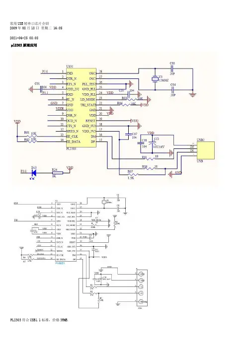
常用USB转串口芯片介绍2009年08月18日星期二 16:05 2021-06-25 08:08pl2303原理应用PL2303符合USB1.1标准,价格3RMB.2 CP2102/CP2103简介Silicon Laboratories公司推出的USB接口与RS232接口转换器CP2102/CP2103是一款高度集成的USB-UART桥接器,提供一个使用最小化元件和PCB空间来实现RS232转换USB的简便解决方案。
如图1所示,CP2102/CP2103包含了一个USB功能控制器、USB收发器、振荡器和带有全部调制解调器控制信号的异步串行数据总线(UART),采用5 mm×5 mm MLP-28的封装。
CP2102/CP2103作为USB/RS232双向转换器,一方面可以从丰机接收USB数据并将其转换为RS232信息流格式发送给外设;另一方面可从RS232外设接收数据转换为USB数据格式传送至主机,其中包括控制和握手信号。
2.1 USB功能控制器和收发器2.2 异步串行数据总线(UART)接口CP2102/CP2103 UART接口包括TX (发送)和RX(接收)数据信号以及RTS、CTS、DSR、DTR、DCD和RI控制信号。
UART支持RTS/CTS、DSR /DTR和X-On/X-Off握手。
通过编程设置UART,支持各种数据格式和波特率。
在PC机的COM端口编程设置UART的数据格式和波特率。
表1为其数据格式和波特率。
2.3 内部EEPROMCP2102/CP2103内部集成有1个EEPROM,用于存储由设备制造商定义的USB供给商ID、产品ID、产品说明、电源参数、器件版本号和器件序列号等信息。
USB配置数据的定义是可选的。
如果EEPROM没有被OEM的数据占用,那么采用表1所示的默认配置数据。
注意,对于可能使用多个基于CP2102/CP2103连接到同一PC机的OEM应用来说,那么需要专用的序列号。
Application Note AC381February 20121© 2012 Microsemi Corporation SmartFusion cSoC: Multi-Channel FFT Co-Processor Using FPGA FabricTable of ContentsIntroductionThe SmartFusion ® customizable system-on-chip (cSoC) device integrates FPGA technology with a hardened ARM ® Cortex™-M3 processor based microcontroller subsystem (MSS) and programmable high-performance analog blocks built on a low power flash semiconductor process. The MSS consists of hardened blocks such as a 100 MHz ARM Cortex-M3 processor, peripheral direct memory access (PDMA), embedded nonvolatile memory (eNVM), embedded SRAM (eSRAM), embedded FlashROM (eFROM), external memory controller (EMC), Watchdog Timer, the Philips Inter-Integrated Circuit (I 2C),serial peripheral interface (SPI), 10/100 Ethernet controller, real-time counter (RTC), GPIO block, fabric interface controller (FIC), in-application programming (IAP), and analog compute engine (ACE).The SmartFusion cSoC device is a good fit for applications that require interface with many analog sensors and analog channels. SmartFusion cSoC devices have a versatile analog front-end (AFE) that complements the ARM Cortex-M3 processor based MSS and general-purpose FPGA fabric. The SmartFusion AFE includes three 12-bit successive approximation register (SAR) ADCs, one first order sigma-delta DAC (SDD) per ADC, high performance signal conditioning blocks, and comparators. The SmartFusion cSoCs have a sophisticated controller for the AFE called the ACE. The ACE configures and sequences all the analog functions using the sample sequencing engine (SSE) and post-processes the results using the post processing engine (PPE) and handles without intervention of Cortex-M3 processor.Refer to the SmartFusion Programmable Analog User’s Guide for more details.This application note describes the capability of SmartFusion cSoC devices to compute the Fast Fourier Transform (FFT) in real time. The Multi Channel FFT example design can be used in medical applications, sensor network applications, multi channel audio Spectrum analyzers, Smart Metering, and sensing applications (such as vibration analysis).This example design uses the Cortex-M3 processor in the SmartFusion MSS as a master and the FFT processor in the FPGA fabric as a slave. All three of the SmartFusion cSoC A2F500’s ADCs are used for data acquisition. The example design uses Microsemi’s CoreFFT IP and the advanced peripheral bus interface (CoreAPB3). A custom-made APB3 interface has been developed to connect CoreFFT with the MSS via CoreAPB3. The Cortex-M3 processor uses the PDMA controller in the MSS for the data transfer and thus helps to free up the Cortex-M3 processor instruction bandwidth.A basic understanding of the SmartFusion design flow is assumed. Refer to Using UART with SmartFusion - Microsemi Libero ® SoC and SoftConsole Flow Tutorial to understand the SmartFusion design flow.Introduction . . . . . . . . . . . . . . . . . . . . . . . . . . . . . . . . . . . . . . . . . . . . . . . . 1Design Overview . . . . . . . . . . . . . . . . . . . . . . . . . . . . . . . . . . . . . . . . . . . . . 2Design Description . . . . . . . . . . . . . . . . . . . . . . . . . . . . . . . . . . . . . . . . . . . . 2Implementing Multi Channel FFT on EVAL KIT BOARD . . . . . . . . . . . . . . . . . . . . . . . . . 7Running the Design . . . . . . . . . . . . . . . . . . . . . . . . . . . . . . . . . . . . . . . . . . . . 8Conclusion . . . . . . . . . . . . . . . . . . . . . . . . . . . . . . . . . . . . . . . . . . . . . . . . 9Appendix A – Design Files . . . . . . . . . . . . . . . . . . . . . . . . . . . . . . . . . . . . . . . 10SmartFusion cSoC: Multi-Channel FFT Co-Processor Using FPGA Fabric2Design OverviewThis design example demonstrates the capability of the SmartFusion cSoC device to compute the FFT for multiple data channels. The FFT computation is a complex task that utilizes extensive logic resources and computation time. In general, for N number of channels, N number of FFT IP’s are needed to be instantiated, which in turn utilize more logic resources on the FPGA. A way to avoid this limitation is to use the same FFT logic for multiple input channels.This design illustrates the implementation of a Multichannel FFT to process multiple data channels through a single FFT and store FFT points in a buffer. The FFT computes the input data read from each channel and stores the N-point result in the respective channel’s allocated buffer. The channel multiplexing is done once each channel buffer has been loaded with the FFT length.Computing frequency components for a real time data of six channels is described in this application note. For sampling the input signals the AFE is used and the complex FFT computation is implemented in the fabric of the SmartFusion cSoC device. The Cortex-M3 processor in the MSS of the SmartFusion cSoC handles the buffer management and channel muxing.Figure 1 depicts the block diagram of six channel FFT co-processor in FPGA fabric.Design DescriptionThe design uses CoreFFT for computing the FFT results. You can download the core generator for CoreFFT at /soc/portal/default.aspx?r=4&p=m=624,ev=60.The design example uses a 512-point and 16-bit FFT. A custom-made APB3 interface has been developed to connect CoreFFT IP with the MSS’s FIC. The CoreFFT output data is stored in a 512x32FIFO within the fabric. The FIFO status signals are given in Table 1 on page 3. The status signals indicate that FFT is ready to receive data and data is available in the output of FIFO. These status signals are mapped to the GPIOs in the MSS. The Cortex-M3 processor can read the GPIOs to handle flow control in the data transfer process from the MSS to CoreFFT.Figure 1 • Multi Channel FFT Block DiagramDesign Description3Figure 2 shows the block diagram of logic in the fabric with custom-made APB3 bus.The data valid signal (ifiD_valid) is generated in custom logic whenever the master needs to write data into the input buffer of the FFT to process through the APB3 interface. The FFT_IP_RDY signal indicates the status of the input buffer of the FFT. If the input buffer is full, the FFT_IP_RDY goes low. The master can read the FFT_IP_RDY signal to get the FFT input buffer status. The FFT generates the processed data with a data valid signal (ifoY_valid). The processed data is stored in the FIFO. When FIFO is not ready to receive output data, it can stop the data fetching from the FFT by pulling down the ifiRead_y signal. The status signal FFT_OP_RDY is used to indicate to the master that processed data is available in the FIFO. FFT_OP_RDY goes High whenever processed data is available in the FFT output buffer.The master can use AEMPTY_OUT or EMPTY_OUT to determine whether the FIFO is empty and all the processed data has been read. Refer to the CoreFFT Handbook for more details on architecture and interface signal descriptions.Three ADCs are configured to have two channels, each channel with 100 ksps sampling rate. The external memory is used for input and output buffers. For each channel, one input buffer having length double to the length of FFT i.e. 1024 words and one output buffer having length equal to the length of FFT i.e. 512 words are used. After each channel's input buffer has 512 points required for the full length of the FFT, each channel, one after the other, streams its points from the FIFO through the FFT. During the FFT computational period, the sampled data values of each channel are stored in the second half of the input buffer. Once the FFT computations for the First half of input buffer completes then the points in the second half of the input buffer will be streamed to FFT. This operation utilizes a ping-pong method. The Cortex-M3 processor is used for data management, that is, buffering the sampled points and data routing or muxing of these values to the FFT computation block. Sampling of the real time data is done by the ACE. The PDMA handles the data transfer between the external SRAM (eSRAM) buffers and CoreFFT logic in FPGA fabric.Figure 2 • CoreFFT with APB Slave InterfaceTable 1 • FIFO Status Signals with DescriptionsSignalDescription FFT_IP_RDYFFT is ready to receive the Input from the master processor FFT_OP_RDYProcessed data is ready in output buffer of FFT AEMPTY_OUTOutput FIFO is almost empty EMPTY_OUT Output FIFO is emptySmartFusion cSoC: Multi-Channel FFT Co-Processor Using FPGA Fabric4Figure 3 shows the implementation of multi channel FFT on the SmartFusion cSoC device.Hardware ImplementationThe MSS is configured with an FIC, clock conditioning circuit (CCC), GPIOs, EMC and a UART. The CCC generates 80 MHz clock, which acts as the clock source. The FIC is configured to use a master interface with an AMBA APB3 interface. Four GPIOs in the MSS are configured as inputs that are used to handle flow control in data transfer from MSS to FFT coprocessor. The EMC is configured for Region 0as Asynchronous RAM and port size as half word. The UART_0 is configured for printing the FFT values to the PC though a serial terminal emulation program.ADC0, ADC1, and ADC2 are configured with 12-bit resolution, two channels and the sampling rate is set to approximately 100 KHz. Figure 4 on page 5 shows the ACE configuration window.Figure 3 • Implementation of Multi Channel FFT on the SmartFusion cSoCDesign Description5The APB wrapper logic is implemented on the top of CoreFFT and connected to CoreAPB3. A FIFO of size 512*32 is used to connect to CoreFFT output.CoreAPB3 acts as a bridge between the MSS and the FFT coprocessor block. It provides an advanced microcontroller bus architecture (AMBA3) advanced peripheral bus (APB3) fabric supporting up to 16APB slaves. This design example uses one slave slot (Slot 0) to interface with the FFT coprocessor block and is configured with direct addressing mode. Refer to the CoreAPB3 Handbook for more details on CoreAPB3 IP .For more details on how to connect FPGA logic MSS, refer to the Connecting User Logic to the SmartFusion Microcontroller Subsystem application note.The logic in the FPGA fabric consumes 18 RAM blocks out of 24. We cannot use eSRAM blocks for implementing CoreFFT as the transactions between these SRAM blocks and FFT logic are very high and are time critical.Figure 5 on page 6 illustrates the multi channel FFT example design in the SmartDesign.Figure 4 • Configure ACESmartFusion cSoC: Multi-Channel FFT Co-Processor Using FPGA Fabric6Table 2 summarizes the logic resource utilization of the design on the A2F500M3F device.Software ImplementationThe Cortex-M3 processor continuously reads the values from ACE and stores the values into the input buffers. If the first 512 points are filled then the processor initiates the FFT process. In the FFT process,the input buffers are streamed one after other to the CoreFFT with the help of PDMA. Using another channel of PDMA the output of FFT is moved to the corresponding channel output buffers.During the FFT process the Cortex-M3 processor stores the sampled values into the second half of the input buffers. Once the FFT process completes the first half of input buffer, then the second half of the input buffer are streamed to CoreFFT.Figure 5 • SmartDesign Implementation of Multi Channel FFTTable 2 • Logic Utilization of the Design on A2F500M3FCoreFFTOther Logic in Fabric Total Ram Blocks14418 (75%)Tiles 78424718313 (72.1%)Implementing Multi Channel FFT on EVAL KIT BOARD7The CALL_FFT(int *) application programmable interface (API) initiates the PDMA to transfer input buffer data to the FFT in the fabric. Before initiating PDMA it checks for FFT whether or not it is ready to read the data. The CALL_FFT(int *) API also checks if the output FIFO is empty so that all the FFT out values have been already read. When the input buffer has points equal to the full length of FFT, then it will be called.The Read_FFT() API initiates the PDMA for reading the FFT output values from FIFO in fabric to the corresponding output buffer. After reading all the values it calls the CALL_FFT() API with the next channel buffer to compute the FFT for next channel. This is done for all channels. After completion of FFT computation for all channels, if the continuous variable is not defined, it will print the FFT output values on the serial terminal. When FFT_OP_READY interrupt occurs then this API will be called.The GPIO1_IRQHandler() interrupt service routine occurs on the positive edge of FFT_OP_READY signal. It calls Read_FFT() API. This interrupt mechanism is used to read the sample values continuously while computing the FFT.If continuous variable is defined, then the FFT is computed without any loss of data samples. If #define continuous line is commented then after every completion of FFT computation of all channels the FFT output is printed on serial terminal. The printed values are in the form of complex numbers.The ping-pong mechanism is used for input data buffer to store the samples continuously. For each channel the input buffer length is double of the full FFT length. While computing the FFT for the first half of the buffer, the new sample values are stored in the second half of the input buffer and while computing the FFT for second half of buffer, the new sample values are stored in first half of the input buffer.Customizing the Number of ChannelsYou can change the design depending on your requirement. Configure the ADC (Figure 4 on page 5)with the required number of channels and required sampling rate. In SoftConsole project change the parameter value NUM_CHANNELS according to the ADC configuration. Edit the main code for reading ADCs data into buffers according to ACE configuration.Throughput CalculationsThe actual time to get 512 samples with 100 ksps is 5.12 ms. Each channel is configured to 100 ksps, so for every 5.12 ms we will have 512 samples in the input buffers.The actual time taken to compute the FFT for each channel is the sum of time taken to transfer 512points to CoreFFT, FFT computation time, and time to read FFT output to the output buffer.•Total time for computing FFT = (time taken to receive 512 data + computational latency for 512points + time taken to store 512 data) = 512*5 + 23292 + 512*5 =28412 clks •Time to compute FFT for 6 channels = 28412*6 = 170472 clksTime to compute FFT for six channels is 2.1309 ms (If CLK is 80 MHz). It is less than half the sample rate of 5.12 ms.If only one channel is configured with maximum sampling rate (600 ksps) then time to get 512 samples with 600 ksps is 0.853 ms. Time to compute FFT for these 512 samples is 0.355 ms. If you configure three ADCs with maximum sampling rate (1800 ksps) then time to compute the FFT for these three channels will be 1.065 ms which is higher than the sampling time. In this there is a loss of some samples.The design works fine up to 1440 ksps.Implementing Multi Channel FFT on EVAL KIT BOARDTo implement the design on the SmartFusion Evaluation Kit Board the FFT must be 256 point and 8 bit because the A2F200 device has less RAM blocks and logic cells. The ADC channels must be selected for only ADC0 and ADC1. Figure 6 on page 8 shows the implementation of multi channel FFT on the SmartFusion cSoC (A2F200M3F) device.SmartFusion cSoC: Multi-Channel FFT Co-Processor Using FPGA Fabric8Table 3 summarizes the logic resource utilization of the design with 256 points 8-bit FFT on A2F200M3F device.Running the DesignProgram the SmartFusion Evaluation Kit Board or the SmartFusion Development Kit Board with the generated or provided *.stp file (refer to "Appendix A – Design Files" on page 10) using FlashPro and then power cycle the board.For computing continuous FFT values for the all six signals sampled through the ADCs, uncomment the line #define continuous in the main program. The FFT output values are stored in the rdata buffer. This buffer is updated for every computation of FFT.For printing the FFT values on serial terminal (HyperTerminal or PuTTy), comment the line #define continuous in the main program.Figure 6 • Implementation of Multi Channel FFT on the SmartFusion Evaluation Kit BoardTable 3 • Logic Utilization of the Design on A2F200M3F DeviceCoreFFTOther Logic in Fabric Total Ram Blocks718 (100%)Tiles 3201853286 (66%)Conclusion9Connect the analog inputs to the SmartFusion Kit Board with the information provided in Table 4.Invoke the SoftConsole IDE, by clicking on Write Application code under Develop Firmware in Libero ®System-on-Chip (SoC) project (refer to "Appendix A – Design Files") and launch the debugger. Start HyperTerminal or PuTTY with a baud rate of 57600, 8 data bits, 1 stop bit, no parity, and no flow control.If your PC does not have the HyperTerminal program, use any free serial terminal emulation program such as PuTTY or Tera Term. Refer to the Configuring Serial Terminal Emulation Programs Tutorial for configuring the HyperTerminal, Tera Term, or PuTTY .ConclusionThis application note describes the capability of the SmartFusion cSoC devices to compute the multi channel FFT. The Cortex-M3 processor, AFE, and FPGA fabric together gives a single chip solution for real time multi channel FFT system. This design example also shows the 6-channel data acquisition system.Table 4 • SettingsChannelEvaluation Kit Development Kit Channel 173 of J21 (signal header)ADC0 of JP4Channel 274 of J21 (signal header)ADC1 of JP4Channel 377 of J21 (signal header)77 of J21 (signal header)Channel 478 of J21 (signal header)78 of J21 (signal header)Channel 585 of J21 (signal header)Channel 686 of J21 (signal header)Figure 7 • FFT Output Data for 1 kHz Sinusoidal Signal on PUTTYSmartFusion cSoC: Multi-Channel FFT Co-Processor Using FPGA Fabric10Appendix A – Design FilesThe Design files are available for download on the Microsemi SoC Product Groups website:/soc/download/rsc/?f=A2F_AC381_DF.The design zip file consists of Libero SoC projects and programming file (*.stp) for A2F200 and A2F500.Refer to the Readme.txt file included in the design file for directory structure and description.51900249-0/02.12© 2012 Microsemi Corporation. All rights reserved. Microsemi and the Microsemi logo are trademarks of Microsemi Corporation. All other trademarks and service marks are the property of their respective owners.Microsemi Corporation (NASDAQ: MSCC) offers a comprehensive portfolio of semiconductor solutions for: aerospace, defense and security; enterprise and communications; and industrial and alternative energy markets. Products include high-performance, high-reliability analog and RF devices, mixed signal and RF integrated circuits, customizable SoCs, FPGAs, and complete subsystems. Microsemi is headquartered in Aliso Viejo, Calif. Learn more at .Microsemi Corporate HeadquartersOne Enterprise, Aliso Viejo CA 92656 USAWithin the USA: +1 (949) 380-6100Sales: +1 (949) 380-6136Fax: +1 (949) 215-4996。
重要的安全事项(针对火灾、电击或伤害人体的指示)注意-使用该电器产品时,有以下基本的预防措施:1.使用该产品前请详细阅读全部的安全事项;2.本产品应当接地,如果出现故障时,电流经最小的接地电阻流入大地,以减小电击;本产品的电源线和电源插头都配备安全接地,电源插头应当牢固插入适当的电源座,此电源座应当完全按当地的条例来安装和接地。
警告-接地装置连接不当会导致电击;如果你对产品是否正确接地存在疑问,请委托合格电工或维修人员检查;请不要尝试私自更改产品的电源插头,如果不适合电源插座,可委托合格电工安装适当的电源插座;3. 为了减小伤害的风险,当产品在小孩附近使用时,要严密监管;4. 请勿在湿度很大的地方使用机器,例如靠近浴缸、洗面盆、厨房水槽、湿度大的地下室或者靠近游泳池和湖泊;5. 该产品应当安装与通风良好的地方;6. 该产品必须远离热源,例如电暖炉、电热毯或者其他产生热量的产品;7. 该产品的电源类型必须符合操作知识或者产品上标明的类型;8. 该产品要配备一条两端的电源线(一段的插片长过另一端)。
这是安全装置。
如果你无法把电源插头插入电源插座,请联系电工来更换旧插座。
9. 长时间不使用时,请把电源线从电源插座中拔出,从电源插座拔出电源线时,请勿拉扯电源线,应当抓住电源插头将其拔出;10. 细心护理,请勿让杂物或者液体从其缝隙掉进机器内;11. 当有下列情况时,应委托合格维修人员修理:A.电源线或电源插头已被损坏B.杂物或者液体已掉进机内C.产品已被雨淋D.产品已不能正常操作或在演出中出现明显变化E.产品已跌坏或外观损坏12. 当出现在用户维修指南中没有描述的情况时,请勿尝试私自修理,应当委托合格的维修人员修理;13. 警告-勿让重物积压或踩踏电源线,切忌拉、拔或强力扭曲电源线。
请勿滥用电源线,不合格的电源线可能导致火灾或对人构成伤害。
目录重要的安全事项(针对火灾、电击或伤害人体的指示) (1)目录 (2)说明 (3)一、设备架构 (4)二、软件操作说明 (5)2.1 菜单栏和工具栏 (5)2.1.1文件 (5)2.1.2本地设置 (6)2.1.3设备设置 (6)1)用户管理 (6)2)场景管理 (7)3)网络设置 (7)4)串口设置 (7)5)语音跟踪 (7)6)GPIO (8)7)设备升级 (13)2.2 电平显示 (13)2.3 音频输入模块 (13)2.3.1输入源 (14)2.3.2扩展器 (15)2.3.3均衡器 (16)2.3.4压缩器 (16)2.3.5自动增益 (17)2.4场景管理和GPIO (17)2.5自动混音器 (18)2.5闪避器 (19)2.6 SPL控制(自动噪音消除) (20)2.7 混音器 (22)2.8 输出混音器 (22)2.9电话控制 (22)2.10 音频输出模块 (23)2.10.1音箱管理 (24)2.10.2反馈消除器 (25)2.10.3 限幅器 (25)三、技术指标 (26)四、常见问题 (27)说明该系列一共16个型号,各型号功能如下所示:型号输入通道输出通道基本功能反馈消除回声消除电话自动混音440/S 4 4 √880/S 8 8 √1208/S 12 8 √√1212/S 12 12 √√440/A 4 4 √√880/A 8 8 √√1208/A 12 8 √√√1212/A 12 12 √√√440/C 4 4 √√√880/C 8 8 √√√1208/C 12 8 √√√√S1212/C 12 12 √√√√440/TC 4 4 √√√√880/TC 8 8 √√√√1208/TC 12 8 √√√√√1212/TC 12 12 √√√√√注:说明书中的图片和功能说明是按照1212/TC系列,其他型号稍有差异。
实用标准NEUSOFT PACS/RIS v2.1 CONFORMANCE STATEMENT for DICOM V3.0Shenyang Neusoft Co. Ltd2003.7.TABLE OF CONTENTSSection One DICOM Sending and Receiving Service (3)1 Introduction (3)2 Implementation Model (4)2.1 Application Data Flow Diagram (4)2.2 Functional definitions of AE (6)2.3 Equencing of Real-World Activities (6)3 AE Specifications (7)3.1 Dicom Gateway AE Specifications (7)3.2 Association establishment Policies (9)4 Communication Profile (25)5 Extensions/specializations/privatizations (25)6 Configuation (26)7 Support of the Extended Character Sets (27)8 Security Profiles (27)Section Two Study Root Query/Retrieve Information Model Definition (27)4 Introduction (27)5 Information Model Description (28)6 Information Model ENTITY-RELATIONSHIP MODEL (28)3.1 Entity Descriptions (29)3.2 DICOM Gateway Mapping of DICOM Entities (29)4 Information Model Keys (30)4.1 Supported Matching (30)4.2 Study Level (30)4.3 Series Level (31)4.4 Image Level (32)4.5 Private data dictionary (34)Section Three DICOM Print Conference Statement (34)1. Introduction (34)2. Implementation Model (35)2.1 Application Data Flow Diagram (35)2.2 Functional Definition of AE (36)2.3 Sequencing of Real-World Activity (36)2.4 AE Specifications (38)2.5 Communication Profile (41)2.6 Extensions/ Specializations / Privatizations (42)2.7 Configuration (42)2.8 Support of Extended Character Sets (44)2.9 Security Profile (44)Section One DICOM Sending and Receiving Service 1 Introduction本部分主要是介绍NEUSOFT PACS/RIS 2.1 产品里的预处理系统(DICOM网关)在存储方面的特色和一些DICOM说明。
东软秘密东软睿驰7917-500605双预警产品使用说明书东软睿驰汽车技术(上海)有限公司目录1.概述 (1)1.1产品说明 (1)1.2参考标准 (1)1.3术语及缩略语 (1)2.产品组成 (1)3.功能说明 (3)3.1LDW (3)3.2FCW (4)4.限制说明 (5)1.概述1.1产品说明东软睿驰7917-500605双预警产品适用于N2、N3类牵引车,采用雷达、摄像头检测车辆前方车辆、行人、车道线,提供FCW、LDW双预警功能。
1.2参考标准GB/T26773:2011智能运输系统车道偏离预警系统性能要求与检测方法JT-T883-2014营运车辆行驶危险预警系统技术要求和试验方法GB∕T33577-2017智能运输系统车辆前向碰撞预警系统性能要求和测试规程1.3术语及缩略语序号术语中文全称1FCW前方碰撞预警2LDW车道偏离预警3自车安装有双预警产品的车辆4前车位于自车行驶路径前方的车辆2.产品组成东软睿驰7917-500605双预警产品的包含如下关键部件。
表一.双预警产品组成表序号部件数量1一体机控制器12毫米波雷达1图一.产品组成、连接图其中一体机控制器连接车身CAN网络,采集车身信号进行驾驶行为判断,输出LDW、FCW功能报警;集成前视摄像头采集车辆前方视频;通过私有CAN连接毫米波雷达,接收雷达检测结果。
一体机控制器参数表如下表二.控制器参数序号项目技术参数1工作电压24V2工作电压范围18V~32V3额定功率8.5W4最大功率16W5工作温度(-40~+85)℃6存储温度(-40~+95)℃摄像头参数表如下:表三.摄像头参数序号配置规格1传感器OV106402分辨率1280x10803传感器类型CMOS4镜头Sunny4083A5帧频30fps6水平视场角52°±1°7垂直视场角43.4°±1°8工作温度(-40~+85)℃9存储温度(-40~+95)℃毫米波雷达参数如下:表四.雷达参数序号配置规格1额定电压12V2工作电压范围(9~16)V3温度范围-30℃~80℃4存储温度-40℃~90℃3.功能说明3.1LDW车道偏离预警功能基于前视摄像头的图像,识别图像中的车道线,计算自车与车道线的相对位置,据此判断是否发生车道偏离,并在驾驶员无意识偏离车道时发出报警提示。
CS1238用户手册24-bit Sigma-Delta ADC Rev 1.1通讯地址:深圳市南山区蛇口南海大道1079号花园城数码大厦A座9楼邮政编码:518067公司电话:+(86 755)86169257传真:+(86 755)86169057公司网站:微信号:芯海科技微信二维码:版本历史目录版本历史 (2)目录 (3)1芯片功能说明 (5)1.1芯片主要功能特性 (5)1.2芯片应用场合 (5)1.3芯片基本结构功能描述 (6)1.4芯片绝对最大极限值 (7)1.5CS1238 数字逻辑特性 (7)1.6CS1238电气特性 (8)1.7芯片引脚 (9)2芯片功能模块描述 (10)2.1模拟输入前端 (10)2.2温度传感器 (10)2.3低噪声PGA放大器 (11)2.4时钟信号源 (12)2.5复位和断电(POR&power down) (12)2.6SPI串口通信 (13)2.6.1建立时间 (13)2.6.2ADC数据输出速率 (14)2.6.3数据格式 (14)DRDY/) (14)2.6.4数据准备/数据输入输出(DOUT2.6.5串行时钟输入(SCLK) (14)2.6.6数据发送 (15)2.6.7功能配置 (16)2.6.7.1SPI命令字 (16)2.6.7.2SPI寄存器 (17)2.6.8Power down模式 (18)3芯片的封装 (19)3.1SOP-14pin (19)3.2DIP-14pin (19)图目录图1CS1238原理框图 (6)图2CS1238芯片引脚图 (9)图3模拟输入结构图 (10)图4PGA结构图 (11)图5CS1238数据建立过程1 (13)图6CS1238数据建立过程2 (13)图7CS1238读取数据时序图1 (15)图8CS1238读取数据时序图2 (15)图9功能配置时序图 (16)图10CS1238 PowerDown模式示意图 (18)图11芯片SOP14封装尺寸信息 (19)图12芯片DIP14封装尺寸信息 (20)表目录表1CS1238 极限值 (7)表2CS1238数字逻辑特性 (7)表3CS1238电气特性(VDD =5V、3.3V ) (8)表4CS1238电源电气特性(VDD =5V) (8)表5CS1238电源电气特性(VDD = 3.3V) (8)表6PIN脚说明 (9)表7输出速率设置 (14)表8理想输出码和输入信号(1) (14)表9读取数据时序表 (15)表10CS1238命令字说明表 (16)表11Config寄存器说明表 (17)1芯片功能说明CS1238是一款高精度、低功耗模数转换芯片,两路差分输入通道,内置温度传感器和高精度振荡器。
东软云HIS医院管理信息系统V3.0-硬件及服务配置说明系列推荐用户产品型号数据库服务器主机类型小型机或X86 PC 服务器CPU :16Core 3.0GHz 以上RISC CPU 或4*Intel E7-4850v4(16Core ,40M Cache ,2.1GHz )及以上内存:256GB 内置硬盘:2*600GB RAID1网络:千兆操作系统:UNIX 或Linux 6.5企业版64Bit 数据库:Oracle 11gR2配置参数:cursor_sharing = EXACT db_writer_processes = 6job_queue_ processes = 1000open_cursors = 300pga_aggregate_target = 0pre_page_sga = FALSE Processes = 1000Sessions = 1200应用服务器主机类型X86 PC 服务器CPU :8 Core CPU 内存:32G 内置硬盘:200GB 网络:千兆操作系统:Linux 6.5企业版64Bit 中间件服务:Weblogic11g 应用服务负载均衡器主机类型X86 PC 服务器CPU :16 Core CPU 内存:32G 内置硬盘:200GB 网络:千兆操作系统:Linux 6.5企业版64Bit中间件服务:Weblogic11g主机类型X86 PC 服务器CPU :8 Core CPU 硬件配置软件1.2000家的配置硬件配置软件硬件配置软件器(2台)标准级市级医院医疗机构云HIS医疗卫生信息管理系统V3.0(4-6台做RAC )(15~20台集群,可采用虚拟主机)(4台,负载均衡,可采用虚拟主机)。
东软人才实训中心 E-mail:drttc@NEUEBD-ARM 开发套件功能介绍定位选用LPC21xx 系列ARM 开发产品的工程师;组建嵌入式系统教学与开发实验室;有购买能力的个人。
概述NEUEBD-ARM 开发板是沈阳东软集团人才实训中心设计的嵌入式系列开发套件之一,采用PHILIPS 公司基于ARM7TDMI-S 核、单电源供电、LQFP48封装的LPC2103,具有JTAG 仿真调试、ISP 编程等功能。
开发板上提供了一些键盘、LED 、蜂鸣器等常用功能部件,还具有RS232接口电路、I 2C 存储器电路。
另外,用户也可以灵活的跳线组合(开发板内使用的所有I/O 均可断开连接),还有用户I/O 接口,极大地方便了用户进行32位ARM 嵌入式系统的开发实验。
参考照片NEUEBD-ARM 实验板功能特点完全自主设计的软硬件、拥有版权的JTAG 仿真技术;支持ADS1.2集成开发环境的仿真与开发;多种免费商业化软件包及其详细的开发文档:所有I/O 口全部引出,方便用户连接外部电路的开发与使用;可进行GPIO 的控制实验,如键盘输入、蜂鸣器控制、模拟SPI 等;6个独立按键(可用于外部中断、定时器捕获输入),8个LED 指示灯;具有RS232转换电路,可与上位机进行通讯,完成UART 通讯实验;具有I 2C 接口和SPI/SSP 接口输出;可进行外部中断实验,学习向量中断控制器(VIC);定时器控制实验,如定时控制LED 、定时器捕获等;使用板内的CAT1025(内含复位功能),完成I 2C 总线的实验;使用74HC595芯片,实现SPI接口数据发送、接收实验;A/D转换实验;DAC转换实验(更换CPU为LPC2132及以上);实时时钟控制实验;WDT及低功耗控制实验;若干个基础实验及其大量的软件包,完整地验证了几乎所有的硬件功能资源;详细的配套资料。
JTAG仿真器性能介绍和特性JTAG是一款高性能/低价格的ARM内核仿真器,内部采用了最新Flash更新技术,可以使JTAG不断支持新的ARM内核仿真。
V2201 SeriesComponent Compatibility GuideA list of peripheral components suitable for use with the V2201 Series computers2019/02/19 Version 2.3© 2019 Moxa Inc. All rights reserved.Copyright Notice©2018 Moxa Inc.All rights reserved.TrademarksThe MOXA logo is a registered trademark of Moxa Inc.All other trademarks or registered marks in this manual belong to their respective manufacturers.DisclaimerInformation in this document is subject to change without notice and does not represent a commitment on the part of Moxa.Moxa provides this document as is, without warranty of any kind, either expressed or implied, including, but not limited to, its particular purpose. Moxa reserves the right to make improvements and/or changes to this manual, or to the products and/or the programs described in this manual, at any time.Information provided in this manual is intended to be accurate and reliable. However, Moxa assumes no responsibility for its use, or for any infringements on the rights of third parties that may result from its use.This document might contain unintentional technical or typographical errors. Changes are periodically made to the information herein to correct such errors, and these changes are incorporated into new editions of the publication.Technical Support Contact Information/supportMoxa AmericasToll-free: 1-888-669-2872 Tel: +1-714-528-6777 Fax: +1-714-528-6778 Moxa China (Shanghai office) Toll-free: 800-820-5036Tel: +86-21-5258-9955Fax: +86-21-5258-5505Moxa EuropeTel: +49-89-3 70 03 99-0 Fax: +49-89-3 70 03 99-99 Moxa Asia-Pacific Tel: +886-2-8919-1230 Fax: +886-2-8919-1231Moxa IndiaTel: +91-80-4172-9088 Fax: +91-80-4132-10451. IntroductionThis document lists hardware components that are proven to provide the performance listed in the specification when used with the Moxa V2201 Series embedded computers, or computers that share basic design features with the V2201 Series. Moxa computers come with multiple peripheral options and are engineered to work with components having different hardware specifications. This flexibility could sometimes lead to compatibility issues. When used with the V2201 Series embedded computers, peripherals from one manufacturer may not work as well as the ones made by another manufacturer. Moxa provides this list of V2201 Series-compatible components, so that users can be certain of a reliable performance from the V2201 Series, when used with the components listed in this document.2. Testing MethodsTo validate that a component meets the Moxa standards for quality and performance, the following five key compatibility tests are run:∙Ambient temperature burn-in∙Low temperature hard start∙Heat/humidity burn-in∙Cyclic high-low temperature burn-in∙Vibration testAmbient Temperature Burn-InThe component is mounted on to a V2201 computer and put through a series of stress tests at an ambient temperature of around 25˚C, for a specified period of time. The duration of the test is determined based on the class of peripherals being tested.Low Temperature Hard StartThe component is mounted on to an unpowered V2201 computer and then the system is booted up at an extremely low temperature. The designated low temperature value depends on the computer model being tested.Heat/Humidity Burn-InThe component is mounted on to a V2201 computer, placed in a temperature- andhumidity-controlled enclosure, and then put through the burn-in test for a specified period of time. The temperature, humidity, and time targets vary depending on the specification of the computer model used in the test.Cyclic High-Low Temperature Burn-InThe component is mounted on to a V2201 computer, placed in a temperature controlled enclosure, and then put through the burn-in test wherein the temperature is cyclically varied from very high to very low and back again, over a specified period of time. The target temperature range and the duration of the test can vary depending on the specification of the computer model used in the test. Vibration TestThe component is mounted on to a V2201 computer that is bound inside an electromagnetic vibrator, and then put through random vibration tests along three orthogonal axes: longitudinal, transverse, and vertical. The vibration tests are compliant with the EN50155/IEC61373 vibration standards.3. Storage EnduranceStorage media, such as SSDs, CF cards, SD cards, Disk on Module, and CFast, are composed of different electrical components. The main electrical components in these storage media, the NAND-flash memory and NAND-flash controller, impact the storage endurance and lifespan of the storage media.NAND-Flash Memory EnduranceNAND-flash memories have a limit on the number of times they can be programmed and erased (P/E). The P/E cycle as well as the erase count of a NAND-flash memory can be used to determine this limit. For example, an SLC (single-level cell) flash memory has a 60,000 P/E cycle, an MLC (multi-level cell) flash memory has a 3,000 P/E cycle, and TLC NAND flash memories have P/E cycle values up to 1,000. Each flash memory type has a different endurance level, which is why the storage lifespan is based on the flash memory type. Storage that uses SLC type flash memory could have the best endurance level compared with the MLC type storage. SLC storage usually comes with a 5-year OEM warranty (the actual warranty period depends on the original manufacturer). MLC storage only comes with a 1- to 3-year warranty. The major differences between SLC and MLC are: (a) The SLC NAND flash has a lifespan that is around 20 times that of an MLC, and (b) The price can differ by a factor of 4 to 5. The SLC type of storage is recommended for systems that are expected to have high reliability, and for applications that need to frequently write data to a storage medium.Terabytes Written (TBW)TBW is the unit used to evaluate SSD endurance. In actual applications, storage is used for routine operations and data access. Therefore the physical P/E cycle is not appropriate for describing the total rewritable data capacity. The management efficiency of the storage controller also affects the total rewritable data capacity result. For these reasons, Joint Electron Device Engineering Council(JEDEC) has defined a standard for SSD endurance evaluation called JESD218, which uses TBW to measure the endurance of the storage memory. By referring to this TBW value, users can easily estimate the storage specification and select a suitable storage for real-life use cases. For example, when routine operations need a maximum of 20 GB and the expected storage lifespan is 3 years, the total rewritable data demand would be 21.9 TBW (20 GB x 365 x 3). In this case, a storage that has more than 21.9 TBW will meet the requirement. We recommend selecting a storage media with a TBW that is greater than the calculated value.4. Declaration for Liability ExclusionThe specifications, warranty terms, and liability of items listed in this guide are the sole responsibility of the original manufacturers. Moxa does not take any responsibility in this regard. Please visit the manufacturers’ official websites for up-to-date product information before purchasing the components.5. Compatible ComponentsPeripheral components that have been tested and found suitable for use with the V2201 Series computers are listed in this section. The following table lists the Test Codes and their descriptions:。
UNIS R3800 G3服务器操作系统兼容性列表北京紫光恒越网络科技有限公司资料版本:5W100-20180312Copyright © 2018 北京紫光恒越网络科技有限公司及其许可者版权所有,保留一切权利。
未经本公司书面许可,任何单位和个人不得擅自摘抄、复制本书内容的部分或全部,并不得以任何形式传播。
UNIS为北京紫光恒越网络科技有限公司的商标。
对于本手册中出现的其它公司的商标、产品标识及商品名称,由各自权利人拥有。
由于产品版本升级或其他原因,本手册内容有可能变更。
紫光恒越保留在没有任何通知或者提示的情况下对本手册的内容进行修改的权利。
本手册仅作为使用指导,紫光恒越尽全力在本手册中提供准确的信息,但是紫光恒越并不确保手册内容完全没有错误,本手册中的所有陈述、信息和建议也不构成任何明示或暗示的担保。
前言本文介绍UNIS R3800 G3服务器支持的操作系统。
前言部分包含如下内容:•读者对象•本书约定•技术支持•资料意见反馈读者对象本手册主要适用于如下工程师:•网络规划人员•现场技术支持与维护人员•负责服务器配置和维护的网络管理员本书约定1. 命令行格式约定格式意义粗体命令行关键字(命令中保持不变、必须照输的部分)采用加粗字体表示。
斜体命令行参数(命令中必须由实际值进行替代的部分)采用斜体表示。
[ ] 表示用“[ ]”括起来的部分在命令配置时是可选的。
{ x | y | ... }表示从多个选项中仅选取一个。
[ x | y | ... ]表示从多个选项中选取一个或者不选。
{ x | y | ... } *表示从多个选项中至少选取一个。
[ x | y | ... ] *表示从多个选项中选取一个、多个或者不选。
&<1-n>表示符号&前面的参数可以重复输入1~n次。
# 由“#”号开始的行表示为注释行。
2. 图形界面格式约定格式意义< > 带尖括号“< >”表示按钮名,如“单击<确定>按钮”。
东软载波芯片兼容性说明2012.03.28
说明1:东软四代芯片兼容性
东软4代完全兼容3代和3.5代产品,东软08年后的芯片互相完全兼容(包括08年推出的3代、09年推出的3.5代、11年推出的4代)。
说明2:从集中器角度看兼容性(通过切换软件路由模式的方法)
4代集中器,可以抄读4代、3.5代、3代载波表和采集器;
3.5代集中器,可以抄读4代、3.5代、3代载波表和采集器;
3代集中器,可以抄读4代、3.5代、3代、2代载波表和采集器;
2代集中器,可以抄读3代、2代载波表和采集器;
说明3:从载波表和采集器的角度看兼容性(表和采集器不需要任何设置)
4代载波表和采集器,可以被4代、3.5代、3代的集中器抄到;
3.5代载波表和采集器,可以被4代、3.5代、3代的集中器抄到;
3代载波表和采集器,可以被4代、3.5代、3代、2代的集中器抄到;
2代载波表和采集器,可以被3代、2代的集中器抄到;
说明4:东软2代、3代、3.5代、4代方案的载波芯片及路由型号组成
4代 3.5代(逐步停产)3代(逐步停产)2代(已停产)
路由型号RTB-ⅣRTB-Ⅲ-E RT-ⅢRT-Ⅱ
集中器芯片
型号
PLCI38-ⅣPLCI38-Ⅲ-E PLCI38-ⅢPLCI38-Ⅱ
采集器芯片
型号
SSC1641PLCI36GM-Ⅲ-E PLCI36M-ⅢPLCI36M
载波表芯片
型号
PLCI36-Ⅲ-E
PLCI36G-Ⅲ-E
PLCI36M-Ⅲ-E
PLCI36-Ⅲ
ES16-Ⅲ
PLCI36C
说明5:兼容性说明表格(详细)
硬件(集中器芯片及路由硬件)软件(路由运行
模式)
4代
载波表和
采集器
3.5代
载波表和
采集器
3代
载波表和
采集器
2代
载波表和
采集器
4代集中器
(PLCI38-Ⅳ和RTB-Ⅳ)1:标准模式√√√×2:扩展模式√√××3:Ⅲ代模式√√√×4:Ⅳ代模式√×××5:自适应模式√√√×
3.5代集中器
(PLCI38-Ⅲ-E和RT-Ⅲ-E)1:标准模式√√××2:扩展模式√√××3:Ⅲ代模式√√√×
3代集中器(PLCI38-Ⅲ和RT-Ⅲ)Router3模式√√√×Router2模式××√√
2代集中器(PLCI38-
Ⅱ和RT--Ⅱ)
Router2模式××√√√:集中器能够抄到载波表或采集器×:集中器不能抄到载波表或采集器
刘峰(邮箱liufeng@ QQ:135661)
青岛东软载波科技股份有限公司
2012-03-28。