Marking of Diodes_VISHAY
- 格式:pdf
- 大小:91.24 KB
- 文档页数:4
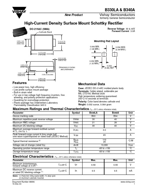
B330LA & B340AVishay Semiconductorsformerly General SemiconductorDocument Number High-Current Density Surface Mount Schottky RectifierReverse Voltage 30 & 40VForward Current 3.0AMounting Pad LayoutMaximum Ratings and Thermal Characteristics (TA= 25°C unless otherwise noted)ParameterSymbol B330LA B340A Unit Device marking codeB33B34V Maximum repetitive peak reverse voltage V RRM 3040V Maximum RMS voltageV RMS 2128V Maximum DC blocking voltageV DC 3040V Maximum average forward rectified current at T L (See Fig. 1)I F(AV) 3.0A Peak forward surge current 8.3ms single halfsine-wave superimposed on rated load (JEDEC Method)I FSM 65A Typical thermal resistance (2)R ΘJA 110R ΘJL 28°C/W Voltage rate of change (rated V R )dv/dt 10,000V/µs Operating junction temperature range T J -65 to +150 °C Storage temperature rangeT STG-65 to +150°CElectrical Characteristics (TA= 25°C unless otherwise noted)ParameterSymbolMax.Max.Unit Maximum instantaneous T J =25°C V F 0.500.55V forward voltage at 3.0A (1)Maximum DC reverse current T J =25°C0.50.5at rated DC blocking voltage (1)I RmANotes : (1) Pulse test: 300µs pulse width, 1% duty cycle(2) Aluminum substrate mounted• Low power loss, high efficiency• Low profile surface mount package • Built-in strain relief• For use in low voltage high frequency inverters, free wheeling, and polarity protection applications • Guardring for overvoltage protection• Plastic package has Underwriters Laboratory Flammability Classification 94V-0Mechanical DataCase:JEDEC DO-214AC molded plastic body Terminals:Solder plated, solderable per MIL-STD750, Method 2026High temperature soldering guaranteed: 250°C/10 seconds at terminalsPolarity:Color band denotes cathode end Weight:0.002 ounce, 0.064 gramDO-214AC (SMA)New Product110100020406080Fig. 3 – Typical Instantaneous Forward CharacteristicsFig. 5 – Typical JunctionCapacitanceNumber of Cycles at 60 H ZReverse Voltage (V)P e a k F o r w a r d S u r g e C u r r e n t (A )0.51.01.52.02.53.03.550Fig. 1 – Forward CurrentDerating CurveA ve r a g e F o rw a r d C u r r e n t (A )Lead T emperature (°C)Fig. 2 – Maximum Non-Repetitive Peak Forward Surge Current0.010.10.20.40.60.81.00.0110100Instantaneous Forward Voltage (V)I n s t a n t a n e o u s F o r w a r d C u r r e n t (A )206040100800.0010.0110.110100Fig. 4 – Typical ReverseCharacteristicsI n s t a n t a n e o u s R e v e r s e C u r r e n t (m A )Percent of Rated Peak Reverse V oltage (%)p F - J u n c t i o n C a p a c i t a n c e1101001001000100.10.30.50.70.9B330LA & B340AVishay Semiconductorsformerly General Semiconductor Document Number 88896Ratings andCharacteristic Curves (T A = 25°C unless otherwise noted)。

ACASA100121001P100ACAS 0612 - ProfessionalVishay BeyschlagProfessional Thin Film Chip Resistor ArrayThe ACAS 0612 thin film chip resistor arrays combine the proven reliability of professional thin film chip resistor products with the advantages of chip resistor arrays. A small package enables the design of high density circuits in combination with reduction of assembly costs. Four equal resistor values or two pairs are available.FEATURES•Advanced thin film technology •Two pairs or four equal resistor values •TCR down to ± 25 ppm/K •Tolerance down to ± 0.5 %•Pure Sn termination on Ni barrier layer•Material categorization: For definitions of compliance please see /doc?99912APPLICATIONS•Voltage divider •Feedback circuits •Signal conditioningNotes(1)Resistance values to be selected from E24; E192.(2)For specified TCR tracking, tolerance matching and even tighter absolute tolerance and TCR please refer to data sheet ACAS 0612 -Precision available on our web site at /doc?28751.TECHNICAL SPECIFICATIONSDESCRIPTION ACAS 0612EIA size 0612Metric sizeRR1632M Configuration, isolated 4 x 0603Design:All equal AE Two pairs TPResistance values 47Ω to 221 k Ω (1)Absolute tolerance (2)± 1 %; ± 0.5 %Absolute temperature coefficient (2)± 50 ppm/K; ± 25 ppm/KMax. resistance ratio R min./R max.1:10Rated dissipation: P 70Element0.1 W Package, 4 x 06030.3 W Operating voltage75 V Permissibe film temperature 125°C Operating temperature range- 55°C to 125 °CInsulation voltage (U ins ) against ambient and between isolated resistors, continuous75 VACAS 0612 - ProfessionalVishay BeyschlagAPPLICATION INFORMATIONThe power dissipation on the resistor generates a temperature rise against the local ambient, depending on the heat flow support of the printed-circuit board (thermal resistance). The rated dissipation applies only if the permitted film temperature is not exceeded. These resistors do not feature a limited lifetime when operated within the permissible limits.CIRCUITSNotes•Products can be ordered using either the PART NUMBER or the PRODUCT DESCRIPTION.(1)R 1 = R 4 ≤ R 2 = R 3.(2)Please refer to the table TEMPERATURE COEFFICIENT AND RESISTANCE RANGE, see next page.(3)Please refer to the table PACKAGING, see next page.DESIGNACAS 0612AE R 1 = R 2 = R 3 = R 4TPR 1 = R 4 < R 2 = R 3PART NUMBER AND PRODUCT DESCRIPTIONPart Number: ACASA110012200P500MODEL/SIZE TERMINAL SIZE RESISTANCE (1)ACCURACY GRADE (2)RESISTANCE (1)PACKAGINGSPECIAL ACAS = Convex squareA = 06123 digit resistance value R 1, R 41 digit multiplier MULTIPLIER 9 = *10-10 = *1001 = *1012 = *1023 = *103TCR and tolerance1233 digit resistance value R 2, R 31 digit multiplier MULTIPLIER 9 = *10-10 = *1001 = *1012 = *1023 = *103P1P500 = StandardProduct Description: ACAS 0612 110R 1220R P5ACA S0612110R 1220R P5MODEL/SIZE TERMINATION SIZE RESISTANCE R 1, R 4 (1)ACCURACY GRADE (2)RESISTANCE R 2, R 3 (1)PACKAGINGACA = ChipArrayS = Convex square0612110R = 110 Ω1K1 = 1.1 k Ω22K1 = 22.1 k ΩTCR and tolerance123220R = 220 Ω1K1 = 1.1 k Ω22K1 = 22.1 k ΩP1P5S A 1100120C A A 2050P 0ACAS 0612 - ProfessionalVishay BeyschlagDIMENSIONSPATTERN STYLES FOR CHIP RESISTOR ARRAYTEMPERATURE COEFFICIENT AND RESISTANCE RANGETYPEACCURACY GRADEABSOLUTE RELATIVERESISTANCEVALUE TCR TOLERANCE TCR TOLERANCEACAS 06121± 25 ppm/K ± 0.5 %--47 Ω to 221 k Ω2± 50 ppm/K ± 0.5 %--47 Ω to 221 k Ω3± 50 ppm/K± 1 %--47 Ω to 221 k ΩPACKAGINGTYPECODE QUANTITY PACKAGING STYLE WIDTHPITCHREEL DIAMETERACAS 0612P11000Tape and reel cardboard tape acc. IEC 60286-3Type I8 mm 4 mm 180 mm/7"P55000DIMENSIONS - Chip resistor array, mass and relevant physical dimensionsTYPE L (mm)W (mm)H (mm)P (mm)A 1(mm)A (mm)T 1(mm)T 2(mm)MASS (mg)ACAS 06121.5 ± 0.153.2 ± 0.150.45 ± 0.10.8 ± 0.10.6 ± 0.10.4 ± 0.10.3 ± 0.150.4 ± 0.156.6RECOMMENDED SOLDER PAD DIMENSIONS FOR CHIP RESISTOR ARRAYSTYPE G (mm)Y (mm)X (mm)U (mm)Z (mm)I (mm)P (mm)ACAS 06120.70.70.640.52.10.30.8ACAS 0612 - Professional Vishay BeyschlagDESCRIPTIONThe production of the components is strictly controlled and follows an extensive set of instructions established for reproducibility. A homogeneous film of metal alloy is deposited on a high grade (Al2O3) ceramic substrate using a mask to separate the adjacent resistors and conditioned to achieve the desired temperature coefficient. Specially designed inner contacts are realized on both sides. A special laser is used to achieve the target value by smoothly cutting a meander groove in the resistive layer without damaging the ceramics.The resistor elements are covered by a protective coating designed for electrical, mechanical and climatic protection. The terminations receive a final pure tin on nickel plating. The result of the determined production is verified by an extensive testing procedure and optical inspection performed on 100 % of the individual chip resistors. Only accepted products are laid directly into the paper tape in accordance with IEC 60286-3 (3).ASSEMBLYThe resistors are suitable for processing on automatic SMD assembly systems. They are suitable for automatic soldering using reflow or vapour phase as shown in IEC 61760-1 (3). The encapsulation is resistant to all cleaning solvents commonly used in the electronics industry, including alcohols, esters and aqueous solutions. The suitability of conformal coatings, if applied, shall be qualified by appropriate means to ensure the long-term stability of the whole system. The resistors are RoHS compliant; the pure tin plating provides compatibility with lead (Pb)-free and lead-containing soldering processes. The permitted storage time is 20 years, whereas the solderability is specified for 2 years after production or requalification. The immunity of the plating against tin whisker growth has been proven under extensive testing.All products comply with the GADSL(1) and the CEFIC-EECA-EICTA(2) list of legal restrictions on hazardous substances. This includes full compliance with the following directives:•2000/53/EC End of Vehicle life Directive (ELV) and Annex II (ELV II)•2011/65/E C Restriction of the use of Hazardous Substances directive (RoHS)•2002/96/E C Waste E lectrical and E lectronic E quipment Directive (WEEE)TESTSWhere applicable, the resistors are tested in accordance with EN140401-801 which refers to EN60115-1 and EN140400.Notes(1)Global Automotive Declarable Substance List, see .(2)CEFIC (European Chemical Industry Council), EECA (European Electronic Component Manufacturers Association), EICTA (European tradeorganisation representing the information and communications technology and consumer electronics), see → policy →environmental policy group → chemicals → jig → Joint Industry Guide (JIG-101 Ed 2.0).(3)The quoted IEC standards are also released as EN standards with the same number and identical contents.ACAS 0612 - Professional Vishay BeyschlagFUNCTIONAL PERFORMANCEACAS 0612 - ProfessionalVishay BeyschlagTESTS AND REQUIREMENTSEssentially all tests are carried out in accordance with the following specifications:EN 60115-1, generic specification EN 140400, sectional specification EN 140401-801, detail specificationThe testing also covers most of the requirements specified by EIA/IS-703 and JIS-C-5202.The tests are carried out in accordance with IEC 60068 (1)and under standard atmospheric conditions according to IEC 60068-1 (1), 5.3. Climatic category LCT/UCT/56 (ratedtemperature range: Lower category temperature, upper category temperature; damp heat, long term, 56 days) is valid (LCT = - 55 °C/UCT = 125 °C).Unless otherwise specified the following values apply:Temperature: 15 °C to 35 °C Relative humidity: 45 % to 75 %Air pressure: 86 kPa to 106 kPa (860 mbar to 1060 mbar)The requirements stated in the “Test Procedures and Requirements” table are based on the required tests and permitted limits of EN 140401-801 where applicable.Notes(1)The quoted IEC standards are also released as EN standards with the same number and identical contents.(2)Figures are given for arrays with equal values, design type AE.(3)For a single element.TEST PROCEDURES AND REQUIREMENTSEN 60115-1CLAUSEIEC 60068-2 (1)TEST METHODTESTPROCEDUREREQUIREMENTS PERMISSIBLE CHANGE (2)(∆R )Stability for product types:ACAS 061247 Ωto 221 k Ω4.5-Resistance -± 1 %; ± 0.5 %4.8.4.2-Temperature coefficientAt (20/- 55/20) °C and(20/125/20) °C ± 50 ppm/K; ± 25 ppm/K 4.25.1-Endurance U = or U = U max.;1.5 h on; 0.5 h off;whichever is the less severe;70 °C; 1000 h± (0.25 % R + 0.05 Ω)4.25.3-Endurance at upper category temperature125°C; 1000 h ± (0.25 % R + 0.05 Ω)4.2478 (Cab)Damp heat,steady state (40± 2) °C; 56days;(93 ± 3) %RH ± (0.5 % R + 0.05 Ω)4.13-Short time overload (3)U = 2.5 x or U = 2x U max.; 5 s ± (0.1 % R + 0.01 Ω)no visible damage 4.1914 (Na)Rapid change of temperature 30min at - 55 °C and 30min at 125 °C;5cycles ± (0.1 % R + 0.01 Ω)no visible damage 4.18.258 (Td)Resistance to solderingheatReflow method 2 (IR/forced gas convection);(260± 5)°C; (10± 1) s ± (0.25 % R + 0.01 Ω)no visible damage4.17.258 (Td)SolderabilitySolder bath method;SnPb; non-activated flux accelerated ageing 4 h/155 °C(215± 3) °C; (3 ± 0.3) s Good tinning (≥ 95 % covered);no visible damageSolder bath method;SnAgCu; non-activated flux accelerated ageing 4 h/155 °C(235± 3) °C; (2 ± 0.2) s4.3221 (Ue 3)Shear (adhesion)45 NNo visible damage 4.3321 (Ue 1)Substrate bendingDepth 2 mm, 3 times ± (0.1 % R + 0.01 Ω)no visible damage;no open circuit in bent position 4.7-Voltage proofU RMS = U ins(60 ± 5)s; against ambient, between adjacent resistorsNo flashover or breakdownP 70 x R P 70 x RLegal Disclaimer Notice VishayDisclaimerALL PRODU CT, PRODU CT SPECIFICATIONS AND DATA ARE SU BJECT TO CHANGE WITHOU T NOTICE TO IMPROVE RELIABILITY, FUNCTION OR DESIGN OR OTHERWISE.Vishay Intertechnology, Inc., its affiliates, agents, and employees, and all persons acting on its or their behalf (collectively,“Vishay”), disclaim any and all liability for any errors, inaccuracies or incompleteness contained in any datasheet or in any other disclosure relating to any product.Vishay makes no warranty, representation or guarantee regarding the suitability of the products for any particular purpose or the continuing production of any product. To the maximum extent permitted by applicable law, Vishay disclaims (i) any and all liability arising out of the application or use of any product, (ii) any and all liability, including without limitation special, consequential or incidental damages, and (iii) any and all implied warranties, including warranties of fitness for particular purpose, non-infringement and merchantability.Statements regarding the suitability of products for certain types of applications are based on Vishay’s knowledge of typical requirements that are often placed on Vishay products in generic applications. Such statements are not binding statements about the suitability of products for a particular application. It is the customer’s responsibility to validate that a particular product with the properties described in the product specification is suitable for use in a particular application. Parameters provided in datasheets and / or specifications may vary in different applications and performance may vary over time. All operating parameters, including typical parameters, must be validated for each customer application by the customer’s technical experts. Product specifications do not expand or otherwise modify Vishay’s terms and conditions of purchase, including but not limited to the warranty expressed therein.Except as expressly indicated in writing, Vishay products are not designed for use in medical, life-saving, or life-sustaining applications or for any other application in which the failure of the Vishay product could result in personal injury or death. Customers using or selling Vishay products not expressly indicated for use in such applications do so at their own risk. Please contact authorized Vishay personnel to obtain written terms and conditions regarding products designed for such applications.No license, express or implied, by estoppel or otherwise, to any intellectual property rights is granted by this document or by any conduct of Vishay. Product names and markings noted herein may be trademarks of their respective owners.© 2019 VISHAY INTERTECHNOLOGY, INC. ALL RIGHTS RESERVEDACASA100121001P100。

5 mm Square Surface Mount Miniature Trimmers Multi-TurnCermet SealedDESIGN SUPPORT TOOLSThe TSM4 trimming potentiometer has been designed for surface mount applications and offers volumetric efficiency 5 mm x 5 mm x 3.7 mm with high performance and stability. The TSM4 design is suitable for both manual or automatic operation, and can withstand vapor phase and reflow soldering techniques.FEATURES•0.25 W at 70 °C•Professional and industrial grade•Wide ohmic range (10 Ω to 1 MΩ)•Low contact resistance variation (2 % or 3 Ω)•Small size for optimum packaging density•Tests according to CECC 41000 or IEC 60393-1•Material categorization: for definitions of compliance please see/doc?99912MECHANICAL SPECIFICATIONSMechanical travel13 turns ± 2 Operating torque (max. Ncm)1End stop torque (Ncm)Clutch action (2 turns max.) Unit weight (max. g)0.15Wiper (actual travel)Positioned at approx. 50 %ENVIRONMENTAL SPECIFICATIONSTemperature range-55 °C to +125 °C Climatic category55/125/56 Sealing Sealed container IP67 MSL level1SOLDERING RECOMMENDATIONSRecommended reflow profile 2, see Application Note /doc?52029Note•Nothing stated herein shall be construed as a guarantee of quality or durabilityPERFORMANCESTESTSCONDITIONSTYPICAL VALUES AND DRIFTS∆R T /R T ∆R 1-2/R 1-2OTHERElectrical endurance1000 h at rated power 90'/30' - ambient temp. 70 °C ± 2 %± 3 %Contact res. variation: ∆ < 1 % Rn Climatic sequence Phase A dry heat 125 °C Phase B damp heat Phase C cold -55 °CPhase D damp heat 5 cycles ± 2 %± 3 %Dielectric strength: 600 V RMS Insulation resistance: > 104 M ΩDamp heat, steady state Temperature 40 °C - RH 93 %56 days± 2 %± 3 %Dielectric strength: 600 V RMS Insulation resistance: > 104 M ΩChange of temperature -55 °C to +125 °C5 cycles ± 1 %∆V 1-2/V 1-3 ≤ ± 2 %Mechanical endurance 100 cycles - rated power ± (3 % + 3 Ω)Shock 50 g - 11 ms3 successive shocks in 3 directions± 1 %∆V 1-2/V 1-3 ≤ ± 1 %Vibration10 Hz to 55 Hz 0.75 mm or 10 g - 6 h± 1 %∆V 1-2/V 1-3 ≤ ± 1 %STANDARD RESISTANCE ELEMENT DATASTANDARD RESISTANCE VALUESLINEAR LAWTYPICAL TCR -55 °C +125 °C MAX. POWER AT 70 °CMAX. WORKINGVOLTAGEMAX. CURRENT THROUGH ELEMENTΩW V mA ppm/°C100.25 1.58158± 100200.25 2.23112500.25 3.53771000.25 5.00502000.257.07355000.2511.2221K 0.2515.815.82K 0.2522.311.25K 0.2535.37.110K 0.2550.0 5.020K 0.2570.7 3.550K 0.25112 2.2100K 0.25158 1.6200K 0.25200 1.0500K 0.082000.41M0.042000.2MARKINGVishay trademark, ohmic value, manufacturing dateThe ohmic value is indicated by a 3 figure code, the first two are significant figures, the third one is the multiplier. Example: 100 = 10 Ω101 = 100 Ω 102 = 1000 Ω 503 = 50 000 ΩORDERING INFORMATION (part number)MODEL STYLE OHMIC VALUE TOLERANCE PACKAGING SPECIAL NUMBER TSM4YJ YL ZJ ZLFrom 10 Ω to 1 M Ω504 = 500 k ΩK = 10 %R10 =reel 500 pieces for ZJ and ZLR05 =reel 250 pieces for YJ and YL On request B25 =box of 50 pieces(If applicable)Given by Vishay for custom designDESCRIPTION (for information only)TSM4YL 500K 10 %TR e3MODELSTYLEVALUETOLERANCESPECIALPACKAGINGLEAD (Pb)-FREERELATED DOCUMENTSAPPLICATION NOTES Potentiometers and Trimmers/doc?51001Guidelines for Vishay Sfernice Resistive and Inductive Components/doc?5202955K4RLM4YSTLegal Disclaimer Notice VishayDisclaimerALL PRODU CT, PRODU CT SPECIFICATIONS AND DATA ARE SU BJECT TO CHANGE WITHOU T NOTICE TO IMPROVE RELIABILITY, FUNCTION OR DESIGN OR OTHERWISE.Vishay Intertechnology, Inc., its affiliates, agents, and employees, and all persons acting on its or their behalf (collectively,“Vishay”), disclaim any and all liability for any errors, inaccuracies or incompleteness contained in any datasheet or in any other disclosure relating to any product.Vishay makes no warranty, representation or guarantee regarding the suitability of the products for any particular purpose or the continuing production of any product. To the maximum extent permitted by applicable law, Vishay disclaims (i) any and all liability arising out of the application or use of any product, (ii) any and all liability, including without limitation special, consequential or incidental damages, and (iii) any and all implied warranties, including warranties of fitness for particular purpose, non-infringement and merchantability.Statements regarding the suitability of products for certain types of applications are based on Vishay's knowledge of typical requirements that are often placed on Vishay products in generic applications. Such statements are not binding statements about the suitability of products for a particular application. It is the customer's responsibility to validate that a particular product with the properties described in the product specification is suitable for use in a particular application. Parameters provided in datasheets and / or specifications may vary in different applications and performance may vary over time. All operating parameters, including typical parameters, must be validated for each customer application by the customer's technical experts. Product specifications do not expand or otherwise modify Vishay's terms and conditions of purchase, including but not limited to the warranty expressed therein.Hyperlinks included in this datasheet may direct users to third-party websites. These links are provided as a convenience and for informational purposes only. Inclusion of these hyperlinks does not constitute an endorsement or an approval by Vishay of any of the products, services or opinions of the corporation, organization or individual associated with the third-party website. Vishay disclaims any and all liability and bears no responsibility for the accuracy, legality or content of the third-party website or for that of subsequent links.Except as expressly indicated in writing, Vishay products are not designed for use in medical, life-saving, or life-sustaining applications or for any other application in which the failure of the Vishay product could result in personal injury or death. Customers using or selling Vishay products not expressly indicated for use in such applications do so at their own risk. Please contact authorized Vishay personnel to obtain written terms and conditions regarding products designed for such applications. No license, express or implied, by estoppel or otherwise, to any intellectual property rights is granted by this document or by any conduct of Vishay. Product names and markings noted herein may be trademarks of their respective owners.© 2023 VISHAY INTERTECHNOLOGY, INC. ALL RIGHTS RESERVED。

21.34 Printed Circuit Board Standards21.34 印刷电路板标准Group I: Cards shall be of glass epoxy construction, comply with requirements of NEMA L1-1 grade FR-4, and have minimum nominal thickness of 0.063 inches.第一组:卡片应该使用玻璃环氧基树脂构造,遵守国际电气制造业协会L1-1等级FR-4的要求,, 最低标称厚度为0.063英寸。
Cards shall have conductors whose material shall be copper. Thickness and width of conductors shall be determined on basis of current carrying capacity and in accordance with IPC 2221A and IPC 2222. Minimum conductor thickness shall be 0.002 inch.卡片应该有材料是铜的半导体。
导体的厚度和宽度取决于电流负载能力的基础上,按照IPC2221A和IPC2222实行。
最小的半导体的厚度应该是0.002英寸。
Printed circuit cards and components shall be covered with conformal coating on both sides between 0.003 inch and 0.007 inch in thickness. provisions to preclude coating from entering sockets shall be taken during the coating process.印刷电路卡片和组件应该被两边的保形涂层所覆盖,厚度在0.003英寸和0.007英寸之间。

1.5KE160CA-E3/54 1.5KE47CA-E3/541.5KE6.8A thru 1.5KE540A, 1N6267A thru 1N6303AVishay General SemiconductorT RANS Z ORB ® Transient Voltage SuppressorsDEVICES FOR BI-DIRECTION APPLICATIONSFor bi-directional types, use CA suffix (e.g. 1.5KE220CA) Electrical characteristics apply in both directions.FEATURES•Glass passivated chip junction•Available in uni-directional and bi-directional •1500 W peak pulse power capability with a 10/1000 μs waveform, repetitive rate (duty cycle): 0.01 %•Excellent clamping capability •Very fast response time•Low incremental surge resistance•AEC-Q101 qualified•Solder dip 275 °C max. 10 s, per JESD 22-B106•Material categorization: for definitions of compliance please see /doc?99912TYPICAL APPLICATIONSUse in sensitive electronics protection against voltage transients induced by inductive load switching and lighting on ICs, MOSFET, signal lines of sensor units for consumer, computer, industrial, automotive, and telecommunication.MECHANICAL DATACase: molded epoxy body over passivated junction Molding compound meets UL 94 V-0 flammability rating Base P/N-E3 - RoHS compliant, commercial gradeBase P/NHE3_X - RoHS compliant, and AEC-Q101 qualified (“X” denotes revision code e.g. A, B, ...)Terminals: matte tin plated leads, solderable per J-STD-002 and JESD 22-B102E3 suffix meets JESD 201 class 1A whisker test, HE3 suffix meets JESD 201 class 2 whisker testNote• 1.5KE250A to 1.5KE540A are commercial grade only•Bi-directional is available from 1.5KE6.8CA to 1.5KE220CA onlyPolarity: For uni-directional types the color band denotes cathode end, no marking on bi-directional typesNotes(1)Non-repetitive current pulse, per fig. 3 and derated above T A= 25 °C per fig. 2(2)Measured on 8.3 ms single half sine-wave or equivalent square wave, duty cycle = 4 pulses per minute maximum (3)V F = 3.5 V for 1.5KE220A and below; V F= 5.0 V for 1.5KE250A and above PRIMARY CHARACTERISTICSV BR uni-directional 6.8 V to 540 V V BR bi-directional 6.8 V to 220 V V WM uni-directional 5.8 V to 459 V V WM bi-directional5.8 V to 185 V P PPM 1500 W P D6.5 W I FSM (uni-directional only)200 A T J max.175 °CPolarity Uni-directional, bi-directionalPackage1.5KEMAXIMUM RATINGS (T A = 25 °C unless otherwise noted)PARAMETERSYMBOL VALUE UNIT Peak pulse power dissipation with a 10/1000 μs waveform (1) (fig. 1)P PPM 1500W Peak pulse current with a 10/1000 μs waveform (1) I PPM See next tableA Power dissipation on infinite heatsink at T L = 75 °C (fig. 5)P D 6.5W Peak forward surge current 8.3 ms single half sine-wave uni-directional only (2)I FSM 200A Maximum instantaneous forward voltage at 100 A for uni-directional only (3) V F 3.5/5.0V Operating junction and storage temperature rangeT J , T STG-55 to +175°C1.5KE6.8A thru 1.5KE540A, 1N6267A thru 1N6303AVishay General SemiconductorNotes(1) Pulse test: t p≤ 50 ms (2) S urge current waveform per fig. 3 and derate per fig. 2(3) All terms and symbols are consistent with ANSI/IEEE CA62.35(4) For bi-directional types with V R 10 V and less the I Dlimit is doubled (+) Underwriters laboratory recognition for the classification of protectors (QVGQ2) under the UL standard for safety 497B and file number E136766 for both uni-directional and bi-directional devicesELECTRICAL CHARACTERISTICS (T A = 25 °C unless otherwise noted)JEDEC ® TYPE NUMBER GENERAL SEMICONDUCTOR PART NUMBER BREAKDOWN VOLTAGE V BR AT I T (1)(V) TEST CURRENT I T (mA)STAND-OFF VOLTAGE V WM (V)MAXIMUM REVERSE LEAKAGE AT V WM I D (4) (μA) MAXIMUM PEAKPULSECURRENT I PPM (2)(A)MAXIMUM CLAMPING VOLTAGE AT I PPM V C (V) MAXIMUM TEMPERATURE COEFFICIENTOF V BR (%/°C)MIN.MAX.1N6267A (+)1.5KE6.8A 6.457.1410 5.80100014310.50.0571N6268A (+)1.5KE7.5A 7.137.8810 6.4050013311.30.0611N6269A (+)1.5KE8.2A 7.798.61107.022*******.10.0651N6270A (+)1.5KE9.1A 8.659.55 1.07.785011213.40.0681N6271A (+)1.5KE10A 9.5010.5 1.08.551010314.50.0731N6272A (+)1.5KE11A 10.511.6 1.09.40 5.096.215.60.0751N6273A (+)1.5KE12A 11.412.6 1.010.2 5.089.816.70.0781N6274A (+)1.5KE13A 12.413.7 1.011.1 5.082.418.20.0811N6275A (+)1.5KE15A 14.315.8 1.012.8 1.070.821.20.0841N6276A (+)1.5KE16A 15.216.8 1.013.6 1.066.722.50.0861N6277A (+)1.5KE18A 17.118.9 1.015.3 1.059.525.20.0891N6278A (+)1.5KE20A 19.021.0 1.017.1 1.054.227.70.0901N6279A (+)1.5KE22A 20.923.1 1.018.8 1.049.030.60.0921N6280A (+)1.5KE24A 22.825.2 1.020.5 1.045.233.20.0941N6281A (+)1.5KE27A 25.728.4 1.023.1 1.040.037.50.0961N6282A (+)1.5KE30A 28.531.5 1.025.6 1.036.241.40.0971N6283A (+)1.5KE33A 31.434.7 1.028.2 1.032.845.70.0981N6284A (+)1.5KE36A 34.237.8 1.030.8 1.030.149.90.0991N6285A (+)1.5KE39A 37.141.0 1.033.3 1.027.853.90.1001N6286A (+)1.5KE43A 40.945.2 1.036.8 1.025.359.30.1011N6287A (+)1.5KE47A 44.749.4 1.040.2 1.023.164.80.1011N6288A (+)1.5KE51A 48.553.6 1.043.6 1.021.470.10.1021N6289A (+)1.5KE56A 53.258.8 1.047.8 1.019.577.00.1031N6290A (+)1.5KE62A 58.965.1 1.053.0 1.017.685.00.1041N6291A (+)1.5KE68A 64.671.4 1.058.1 1.016.392.00.1041N6292A (+)1.5KE75A 71.378.8 1.064.1 1.014.61040.1051N6293A (+)1.5KE82A 77.986.1 1.070.1 1.013.31130.1051N6294A (+)1.5KE91A 86.595.5 1.077.8 1.012.01250.1061N6295A (+)1.5KE100A 95.0105 1.085.5 1.010.91370.1061N6296A (+)1.5KE110A 105116 1.094.0 1.09.91520.1071N6297A (+)1.5KE120A 114126 1.0102 1.09.11650.1071N6298A (+)1.5KE130A 124137 1.0111 1.08.41790.1071N6299A (+)1.5KE150A 143158 1.0128 1.07.22070.1061N6300A (+)1.5KE160A 152168 1.0136 1.0 6.82190.1081N6301A (+)1.5KE170A 162179 1.0145 1.0 6.42340.1081N6302A (+)1.5KE180A 171189 1.0154 1.0 6.12460.1081N6303A (+)1.5KE200A 190210 1.0171 1.0 5.52740.108-(+)1.5KE220A 209231 1.0185 1.0 4.63280.108- 1.5KE250A 237263 1.0214 1.0 4.43440.110- 1.5KE300A 285315 1.0256 1.0 3.64140.110- 1.5KE350A 333368 1.0300 1.0 3.14820.110- 1.5KE400A 380420 1.0342 1.0 2.75480.110- 1.5KE440A 418462 1.0376 1.0 2.56020.110- 1.5KE480A 456504 1.0408 1.0 2.286580.110- 1.5KE510A 485535 1.0434 1.0 2.156980.110- 1.5KE540A 513567 1.0459 1.0 2.037400.1101.5KE6.8A thru 1.5KE540A, 1N6267A thru 1N6303A Vishay General Semiconductor Notes(1)AEC-Q101 qualified(2)Applied for 1.5KE6.8AHE3_A to 1.5KE220AHE3_A, and 1.5KE6.8CAHE3_A to 1.5KE220CAHE3_ARATINGS AND CHARACTERISTICS CURVES (T A = 25 °C unless otherwise noted)Fig. 1 - Peak Pulse Power Rating CurveFig. 2 - Pulse Power or Current vs. Initial Junction TemperatureFig. 3 - Pulse WaveformFig. 4 - Typical Junction CapacitanceTHERMAL CHARACTERISTICS (T A = 25 °C unless otherwise noted)PARAMETER SYMBOL VALUE UNIT Typical thermal resistance, junction to ambient RθJA75°C/ W Typical thermal resistance, junction to lead RθJL15.4ORDERING INFORMATION (Example)PREFERRED PIN UNIT WEIGHT (g)PREFERRED PACKAGE CODE BASE QUANTITY DELIVERY MODE1.5KE6.8A-E3/540.96854140013" diameter paper tape and reel 1.5KE6.8AHE3_A/C (1)(2)0.968C140013" diameter paper tape and reel1.5KE6.8A thru 1.5KE540A, 1N6267A thru 1N6303A Vishay General SemiconductorFig. 5 - Power Derating CurveFig. 6 - Maximum Non-Repetitive Forward Surge CurrentUni-Directional onlyFig. 7 - Incremental Clamping Voltage Curve (Uni-Directional)Fig. 8 - Incremental Clamping Voltage Curve (Uni-directional) Fig. 9 - Incremental Clamping Voltage Curve (Bi-directional) Fig. 10 - Incremental Clamping Voltage Curve (Bi-Directional)1.5KE6.8A thru 1.5KE540A, 1N6267A thru 1N6303A Vishay General SemiconductorFig. 11 - Instantaneous Forward Voltage Characteristics Curve Fig. 12 - Typical Transient Thermal Impedance PACKAGE OUTLINE DIMENSIONS in inches (millimeters)APPLICATION NOTES•This series of Silicon Transient Suppressors is used in applications where large voltage transients can permanently damage voltage-sensitive components.•The TVS diode can be used in applications where induced lightning on rural or remote transmission lines presents a hazard to electronic circuitry (ref: R.E.A. specification P.E. 60). •This Transient Voltage Suppressor diode has a pulse power rating of 1500 W for 1 ms. The response time of TVS diode clamping action is effectively instantaneous (1 x 10⁻⁹ s bi-directional); therefore, they can protect integrated circuits, MOS devices, hybrids, and other voltage sensitive semiconductors and components. TVS diodes can also be used in series or parallel to increase the peak power ratings.Legal Disclaimer Notice VishayDisclaimerALL PRODUCT, PRODUCT SPECIFICAT IONS AND DAT A ARE SUBJECT T O CHANGE WIT HOUT NOT ICE T O IMPROVE RELIABILITY, FUNCTION OR DESIGN OR OTHERWISE.Vishay Intertechnology, Inc., its affiliates, agents, and employees, and all persons acting on its or their behalf (collectively, “Vishay”), disclaim any and all liability for any errors, inaccuracies or incompleteness contained in any datasheet or in any other disclosure relating to any product.Vishay makes no warranty, representation or guarantee regarding the suitability of the products for any particular purpose or the continuing production of any product. To the maximum extent permitted by applicable law, Vishay disclaims (i) any and all liability arising out of the application or use of any product, (ii) any and all liability, including without limitation special, consequential or incidental damages, and (iii) any and all implied warranties, including warranties of fitness for particular purpose, non-infringement and merchantability.Statements regarding the suitability of products for certain types of applications are based on Vishay’s knowledge of typical requirements that are often placed on Vishay products in generic applications. Such statements are not binding statements about the suitability of products for a particular application. It is the customer’s responsibility to validate that a particular product with the properties described in the product specification is suitable for use in a particular application. Parameters provided in datasheets and / or specifications may vary in different applications and performance may vary over time. All operating parameters, including typical parameters, must be validated for each customer application by the customer’s technical experts. Product specifications do not expand or otherwise modify Vishay’s terms and conditions of purchase, including but not limited to the warranty expressed therein.Except as expressly indicated in writing, Vishay products are not designed for use in medical, life-saving, or life-sustaining applications or for any other application in which the failure of the Vishay product could result in personal injury or death. Customers using or selling Vishay products not expressly indicated for use in such applications do so at their own risk. Please contact authorized Vishay personnel to obtain written terms and conditions regarding products designed for such applications.No license, express or implied, by estoppel or otherwise, to any intellectual property rights is granted by this document or by any conduct of Vishay. Product names and markings noted herein may be trademarks of their respective owners.© 2017 VISHAY INTERTECHNOLOGY, INC. ALL RIGHTS RESERVED1.5KE160CA-E3/54 1.5KE47CA-E3/54。
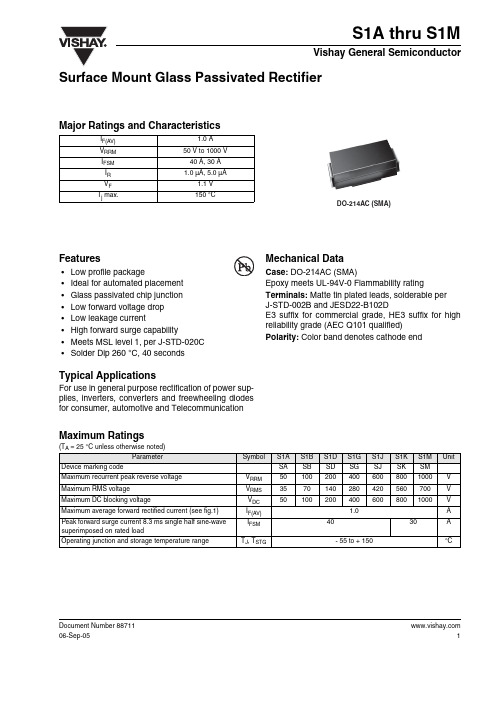
06-Sep-051 2Document Number 8871106-Sep-05S1A thru S1MVishay General SemiconductorElectrical Characteristics(T A = 25°C unless otherwise noted)Thermal Characteristics(T A = 25°C unless otherwise noted)Notes:(1) Thermal resistance from junction to ambient and from junction to lead mounted on P.C.B.with 0.2 x 0.2" (5.0 x 5.0 mm) copper pad areasRatings and Characteristics Curves(T A = 25 °C unless otherwise noted)ParameterTest condition SymbolS1AS1BS1DS1GS1JS1KS1MUnitMaximum instantaneous forward voltageat 1.0 AV F 1.1 V Maximum DC reverse current at Rated DC blocking voltage T A = 25 °C T A = 125 °CI R1.05.0µA50Typical reverse recovery time at I F = 0.5 A, I R = 1.0 A, I rr = 0.25 A t rr 1.8 µsTypical junction capacitanceat 4.0 V , 1 MHzC J 12 pFParameterSymbolS1AS1BS1DS1GS1JS1KS1MUnit Typical thermal resistance (1) R θJA 75 85°C/WR θJL 2730Figure 1. Forward Current Derating Curve Figure 2. Maximum Non-Repetitive Peak Forward Surge CurrentS1A thru S1MDocument Number 8871106-Sep-05Vishay General Semiconductor3Package outline dimensions in inches (millimeters)Figure 3. Typical Instantaneous Forward Characteristics Figure 4. Typical Reverse Leakage CharacteristicsFigure 5. Typical Junction CapacitanceFigure 6. Typical Transient Thermal ImpedanceLegal Disclaimer NoticeVishay Document Number: Revision: 08-Apr-051NoticeSpecifications of the products displayed herein are subject to change without notice. Vishay Intertechnology, Inc., or anyone on its behalf, assumes no responsibility or liability for any errors or inaccuracies.Information contained herein is intended to provide a product description only. No license, express or implied, by estoppel or otherwise, to any intellectual property rights is granted by this document. Except as provided in Vishay's terms and conditions of sale for such products, Vishay assumes no liability whatsoever, and disclaims any express or implied warranty, relating to sale and/or use of Vishay products including liability or warranties relating to fitness for a particular purpose, merchantability, or infringement of any patent, copyright, or other intellectual property right. The products shown herein are not designed for use in medical, life-saving, or life-sustaining applications. Customers using or selling these products for use in such applications do so at their own risk and agree to fully indemnify Vishay for any damages resulting from such improper use or sale.。
THE SMDCODEBOOKSMD Codes.SMD devices are, by their very nature, too small to carry conventional semiconductor type numbers. Instead, a somewhat arbitrary coding system has grown up, wherethe device package carries a simple two- or three-character ID code.Identifying the manufacturers' type number of an SMD device fromthe package code can be a difficult task, involving combing throughmany different databooks.This HTML book is designed to provide an easy means of deviceidentification. It lists well over 3,400 device codes in alphabeticalorder, together with type numbers, device characteristics orequivalents and pinout information.How to use the SMD CodebookTo identify a particular SMD device, first identify the package style and note the ID code printed on the device. Now look up the code in the alphanumeric listing which forms the main part of this book by clicking on the first character shown in the left-menu.Unfortunately, each device code is not necessarily unique. For example a device coded 1A might be either a BC846A or a FMMT3904. Even the same manufacturer may use the same code for different devices!If there is more than one entry, use the package style to differentiate between devices with the same ID code. This compilation has been collected from R P Blackwell G4PMK, manufacturers' data and other sources of SMD device ID codes, pinout and leaded device equivalent information.The entries under the Manufacturer column are not intended to be comprehensive; rather they are intended to provide help on locating sources of more detailed information if you require it.ID Code VariationsMany manufacturers use an extra letter as their own identification code. If the device is from Philips it will sometimes have a lower case 'p' (or sometimes 't') added to the code; Siemens devices usually have a lower case 's'.For example, if the code is 1A, according to the table there are a number of possibilities:• 1A BC846A Phi ITT N BC546A• 1A FMMT3904 Zet N 2N3904• 1A MMBT3904 Mot N 2N3904• 1A IRLML2402 IR F n-ch mosfet 20V 0.9AThis has been a problem in the past, however recently manufacturers have been adding lower case letters which clarify the code.Many recent Motorola devices have a small superscript letter after the device code, such as SA C . (This smaller letter is merely a month of manufacture code.)Many devices from Rohm Semiconductors which start with G have direct equivalents found in the rest of the number. For example GD1 is the same as D1 which is a BCW31.Some devices have a single coloured letter (usually on extremely small diode packages). Colour, if significant, is shown in small type after the code letter.An 'L' suffix usually indicates a low-profile package, such as an SOT323 orSC70.SOT323.SC70.Reverse joggle devices do present a few problems. They oftern have an 'R' in the type number. A reverse package is one where the lead have been bent up instead of down. So it's a mirror image of a conventional device. Identification is usually possible from the code number, but some manufacturers use the same code. In these cases, it's a case of looking at the device with a magnifying glass. The leads of most normal packages come out closer to the circuit board side of the device; conversely a reverse joggle package will have them coming out closer to the 'top' of the device.Sometimes a series of devices, derived from the same die, have related type (not code) numbers. Often an 'R' will indicate a reverse joggle package, and/or a 'W' indicate a smaller package variant, such as SOT343. Sometimes similarities are also found in the code numbers. For example:Recently some manufacturers have used a symbol or lower case letter to indicate the country of manufacture. These have been ignored in the alphabetical ordering. For example:• '67' is the code for a BFP67 (SOT143 package) ,• '67R' is the code for the reverse joggle variant BFP67R (SOT143R),• 'W67' is the code for a SOT343 package version.SOT143.'Z-S' and 'ZtS ' are both 2PC4081Q devices made by Philips; the first made in Hong Kong and the second in Malaysia; this appears in the codebook classified under ZS.Leaded equivalent device and informationWhere possible, the listing gives the part number of a conventional wire-leaded device with equivalent characteristics. If the leaded device is well-known then no more information is given. If the device is less common, some additional information will sometimes be given. Where no exact leaded equivalent exists, a brief device description is given, which may be sufficient to allow substitution with another device.When describing device characteristics, some terms are implied from the type of device. For example, a voltage specified for a rectifier diode is usually the maximum PIV (peak inverse voltage) of the diode, but for a zener diode the operating (zener voltage) will be given.Normally, where a voltage, current or power is specified, these will be limiting values. For example, a device specified as NPN 20V 0.1A 1W is a NPN transistor with a Vce (max) of 20V, maximum collector current of 100mA and a maximum total power dissipation of 1W. Some of the transistors are types with integrated resistors; in the list, a base resistor means a resistor connected in series with the base. When two resistor values are given, the first is the series base resistor, and the second the resistor between base and emitter.Digital Transistors (dtr)These are transistors with built-in resistors.Some have one resistor between base and emitter, others in series with the base. Many others have both.To keep things simple, the series resistor is called R1 and the base emitter resistor is called R2. If both are present, then two values are given, R1 first. So 4k7 + 10k means that R1 (the base resistor) is 4k7 and R2 (the resistor between base and emitter) is 10k.ConclusionIdentifying the manufacturers' type number of an SMD device from the package code can be a difficult task, involving combing through many different databooks. This HTML book is designed to provide an easy means of device identification.Abbreviationsamp amplifieratten attenuatora anodeb basec cathodeca common anodecc common cathodecomp complementd draindg dual gatedtr digital transistor (see codebook introduction) enh enhancement (mode - FETs)fet field effect transistorfT transition frequencyGaAsfet Gallium Arsenide field effect transistorg gategnd groundgp general purposehfe small signal current gaini/p inputId drain currentIg gate currentIr reverse leakage current (diodes)jfet junction field effect transistorMAG maximum available gainmax maximummin minimummmic microwave minature integrated circuit modamp modular amplifier - an mmic amplifier mosfet metal oxide insulated gate fetn-ch n-channel fet (any type)npn npn bipolar transistoro/p outputp-ch p-channel fet (any type)pin pin diodepkg packagepnp pnp bipolar transistorprot protection, protected (as in mosfet gate) res resistors sourceser seriesSi siliconsubstr substratesw switch or switchingVce collector - emitter voltage (maximum) Vcc collector supply voltageManufacturer abbreviationsAgi Agilent (was HP)Fch FairchildHP Hewlett-Packard (Now Agilent)Inf Infineon (was Siemens)ITT ITT SemiconductorsMC Mini-CircuitsMot Motorola (now ON Semiconductors) Nat National SemiconductorNec NECNJRC New Japan Radio CoON ON Semiconductors (was Motorola) Phi PhilipsRoh RohmSGS SGS-ThompsonSie Siemens (now Infineon)Sil Siliconix (Vishay-Silliconix)Tem Temic SemiconductorsTfk Telefunken (Vishay-Telefunken)Tok Toko Inc.Zet ZetexCodes beginning with '0'Code Device Manufacturer Base Package Leaded Equivalent/Data0 2SC3603 Nec CX SOT173 Npn RF fT 7GHz005 SSTPAD5 Sil J - PAD-5 5pA leakage diodep01 PDTA143ET Phi N SOT23 pnp dtr 4k7+4k7t01 PDTA143ET Phi N SOT23 pnp dtr 4k7+4k701 Gali-1 MC AZ SOT89 DC-8GHz MMIC amp 12dB gain 010 SSTPAD10 Sil J - PAD-10 10pA leakage diode 011 SO2369R SGS R SOT23R 2N236902 BST82 Phi M - n-ch mosfet 80V 175mA02 MRF5711L Mot X SOT143 npn RF MRF57102 DTCC114T Roh N - 50V 100mA npn sw + 10k base res 02 Gali-2 MC AZ SOT89 DC-8GHz MMIC amp 16dB gain p02 PDTC143ET Phi N SOT23 npn 4k7+4k7 bias rest02 PDTC143ET Phi N SOT23 npn 4k7+4k7 bias res03 Gali-3 MC AZ SOT89 DC-3GHz MMIC amp 22dB gain 03 DTC143TE Roh N EMT3 npn dtr R1 4k7 50V 100mA03 DTC143TUA Roh N SC70 npn dtr R1 4k7 50V 100mA03 DTC143TKA Roh N SC59 npn dtr R1 4k7 50V 100mA04 DTC114TCA Roh N SOT23 npn dtr R1 10k 50V 100mA 04 DTC114TE Roh N EMT3 npn dtr R1 10k 50V 100mA 04 DTC114TUA Roh N SC70 npn dtr R1 10k 50V 100mA 04 DTC114TKA Roh N SC59 npn dtr R1 10k 50V 100mA 04 MRF5211L Mot X SOT143 pnp RF MRF52104 Gali-4 MC AZ SOT89 DC-4GHz MMIC amp 17.5 dBm -04 PMSS3904 Phi N SOT323 2N3904t04 PMBS3904 Phi N SOT23 2N390405 Gali-4 MC AZ SOT89 DC-4GHz MMIC amp 18 dBm o/p 05 DTC124TE Roh N EMT3 npn dtr R1 22k 50V 100mA 05 DTC124TUA Roh N SC70 npn dtr R1 22k 50V 100mA 05 DTC124TKA Roh N SC59 npn dtr R1 22k 50V 100mA 05F TSDF1205R Tfk WQ - fT12GHz npn 4V 5mA06 Gali-6 MC AZ SOT89 DC-4GHz MMIC amp 115 dBm o/p 06 DTC144TE Roh N EMT3 npn dtr R1 47k 50V 100mA 06 DTC144TUA Roh N SC70 npn dtr R1 47k 50V 100mA 06 DTC144TKA Roh N SC59 npn dtr R1 47k 50V 100mA-06 PMSS3906 Phi N SOT323 2N3906t06 PMBS3906 Phi N SOT23 2N3906020 SSTPAD20 Sil J - PAD-20 20pA leakage diode 050 SSTPAD50 Sil J - PAD-50 50pA leakage diode 081 SO2369AR SGS R SOT23R 2N2369A09 DTC115TUA Roh N SC70 npn dtr R2 100k 50V 100mA 09 DTC115TKA Roh N SC59 npn dtr R2 100k 50V 100mA0A MUN5111DW1 Mot DO SOT363 dual pnp dtr 10k+10k0A DTC125TUA Roh N SC70 npn dtr R2 100k 50V 100mA0A DTC125TKA Roh N SC59 npn dtr R2 100k 50V 100mA0B MUN5112DW1 Mot DO SOT363 dual pnp dtr 22k+22k0C MUN5113DW1 Mot DO SOT363 dual pnp dtr 47k+47k0D MUN5114DW1 Mot DO SOT363 dual pnp dtr 10k+47k0E MUN5115DW1 Mot DO SOT363 dual pnp dtr R1 10k0F MUN5116DW1 Mot DO SOT363 dual pnp dtr R1 4k70G MUN5130DW1 Mot DO SOT363 dual pnp dtr 1k0+1k00H MUN5131DW1 Mot DO SOT363 dual pnp dtr 2k2+2k20J MUN5132DW1 Mot DO SOT363 dual pnp dtr 4k7+4k70K MUN5133DW1 Mot DO SOT363 dual pnp dtr 4k7+47k0L MUN5134DW1 Mot DO SOT363 dual pnp dtr 22k+47k0M MUN5135DW1 Mot DO SOT363 dual pnp dtr 2k2+47kCodes beginning with '1'Code Device Manufacturer Base Package Leaded Equivalent/Data1 2SC3587 Nec CX - npn RF fT10GHz1 BA277 Phi I SOD523 VHF Tuner band switch diode1 (red) BB669 Sie I SOD323 56-2.7 pF varicap10 MRF9411L Mot X SOT143 npn Rf 8GHz MRF94110A PZM10NB2A Phi A SOT346 dual ca 10V 0.3W zener10V PZM10NB Phi C SOT346 10V 0.3W zener10Y BZV49-C10 Phi O SOT89 10V 1W zener11 MRF9511L Mot X SOT143 npn RF 8GHz MRF95111 MUN5311DW1 Mot DP SOT363 npn/pnp dtr 10k+10k11 PDTA114EU Phi N SOT416 pnp dtrp11 PDTA114TT Phi N SOT23 pnp dtrt11 PDTA114TT Phi N SOT23 pnp dtr11A PZM11NB2A Phi A SOT346 dual ca 11V 0.3W zener11A MMBD1501A Nat C SOT23 Si diode 200V 100mA11V PZM11NB Phi C SOT346 11V 0.3W zener11Y BZV49-C11 Phi O SOT89 11V 1W zener12 MUN5312DW1 Mot DP SOT363 npn/pnp dtr 22k+22k12 DTA123EUA Rho N SC70 pnp dtr 2k2+2k2 50V 100ma12 DTA123EKA Rho N SC59 pnp dtr 2k2+2k2 res 50V 100ma p12 PDTC114TT Phi N SOT23 npn dtrt12 PDTC114TT Phi N SOT23 npn dtr12A MMBD1502A Nat K SOT23 Si diode 200V 100mA12A PZM12NB2A Phi A SOT346 dual ca 12V 0.3W zener12E ZC2812E Zet D SOT23 dual series RF schottky15V 20mA 12V PZM12NB Phi C SOT346 12V 0.3W zener12Y BZV49-C12 Phi O SOT89 12V 1W zener13 DTA143EUA Rho N SC70 pnp dtr 4k7+4k7 50V 100ma13 DTA143EKA Rho N SC59 pnp dtr 4k7+4k7 50V 100ma13 DTA143ECA Rho N SOT23 pnp dtr 4k7+4k7 50V 100ma13t BC846BPN Phi N SOT363 BC546B13s BAS125 Sie C SOT23 Schottky sw 24V 100mA13s BAS125W Sie C SOT323 Schottky sw 24V 100mA13 MA4CS103A M/A C SOT23 Schottky RF 20V 100mA13 MUN5313DW1 Mot DP SOT363 npn/pnp dtr 47k+47k13A MMBD1503A Nat D SOT23 dual Si diode 200V 100mA 13A PZM13NB2A Phi A SOT346 dual ca 13V 0.3W zener13E ZC2813E Zet A SOT23 dual ca RF schottky15V 20mA 13V PZM13NB Phi C SOT346 13V 0.3W zener13Y BZV49-C13 Phi O SOT89 13V 1W zener14s BAS125-04 Sie D SOT23 Dual series Schottky 25V 100mA 14s BAS125-04W Sie D SOT323 Dual series Schottky 25V 100mA 14 BAT114-099R Sie DQ - Quad Schottky crossover ring 14 DTA114EUA Roh N SC70 pnp dtr 10k + 10k14 DTA114EKA Roh N SC59 pnp dtr 10k + 10k14 MUN5314DW1 Mot DP SOT363 npn/pnp dtr 10k R114 DTA114ECA Roh N SOT23 pnp dtr 10k + 10k14A MMBD1504A Nat B - dual cc Si diode 200V 100mA 15s BAS125-05 Sie B SOT23 dual cc Schottky 25V 100mA 15s BAS125-05W Sie B SOT323 dual cc Schottky 25V 100mA 15 DTA124EUA Roh N SC70 pnp dtr 30V 50mA 22k+22k 15 DTA124EKA Roh N SC59 pnp dtr 30V 50mA 22k+22k 15 DTA124ECA Roh N SOT23 pnp dtr 30V 50mA 22k+22k 15 MUN5315DW1 Mot DP SOT363 npn/pnp dtr 10k R115 MMBT3960 Mot N - 2N396015A MMBD1505A Nat A - dual ca Si diode 200V 100mA 15A PZM15NB2A Phi A SOT346 dual ca 15V 0.3W zener15V PZM15NB Phi C SOT346 15V 0.3W zener15Y BZV49-C15 Phi O SOT89 15V 1W zenerp16 PDTC114ET Phi N SOT23 npn dtrt16 PDTC114EU Phi N SOT323 npn dtr16s BAS125-06 Sie A SOT23 dual ca Schottky 25V 100mA 16s BAS125-06W Sie A SOT323 dual ca Schottky 25V 100mA 16 MUN5316DW1 Mot DP SOT363 npn/pnp dtr 4k7 R116 DTA144EUA Roh N SC70 pnp dtr 30V 50mA 47k+47k 16 DTA144EKA Roh N SC59 pnp dtr 30V 50mA 47k+47k 16V PZM16NB Phi C SOT346 16V 0.3W zener16Y BZV49-C16 Phi O SOT89 16V 1W zener17s BAS125-07 Sie S SOT143 dual Schottky 25V 100mA 17s BAS125-07W Sie S SOT343 dual Schottky 25V 100mAp17 PDTC124ET Phi N SOT23 npn dtrt17 PDTC124EU Phi N SOT323 npn dtr18 BFP181T Tfk X - npn Rf fT 7.8GHz 10V 20mA 18 PDTC143ZK Phi N SOT346 npn dtr 4k7+47kp18 PDTC143ZT Phi N SOT23 npn dtr 4k7+47kt18 PDTC143ZT Phi N SOT23 npn dtr 4k7+47k18V PZM18NB Phi C SOT346 18V 0.3W zener18Y BZV49-C18 Phi O SOT89 18V 1W zener19 PDTA143ZK Phi N SOT346 pnp dtr 4k7+47k19 DTA115EUA Rho N SC70 pnp dtr 100k+100k 50V 100ma 19 DTA115EKA Rho N SC59 pnp dtr 100k+100k 50V 100ma p19 PDTA143ZT Phi N SOT23 pnp dtr 4k7+47kt19 PDTA143ZT Phi N SOT23 pnp dtr 4k7+47k100 SSTPAD100 Sil J SOT23 PAD-100 100pA leakage diode 101 PZM10NB1 Phi C SOT346 10V 0.3W zener102 PZM10NB2 Phi C SOT346 10V 0.3W zener103 PZM10NB3 Phi C SOT346 10V 0.3W zener111 PZM11NB1 Phi C SOT346 11V 0.3W zener111 DTA113ZUA Roh N SC70 pnp dtr 1k+10k 50V 100mA 112 PZM11NB2 Phi C SOT346 11V 0.3W zener113 PZM11NB3 Phi C SOT346 11V 0.3W zener113 DTA143ZUA Roh N SC70 pnp dtr 4k7+47k 50V 100mA 121 PZM12NB1 Phi C SOT346 12V 0.3W zener121 DTC113ZUA Roh N SC70 npn dtr 1k+10k 50V 100mA 122 PZM12NB2 Phi C SOT346 12V 0.3W zener123 PZM12NB3 Phi C SOT346 12V 0.3W zener123 DTC143ZUA Roh N SC70 npn dtr 4k7+47k 50V 100mA 131 PZM13NB1 Phi C SOT346 13V 0.3W zener132 PZM13NB2 Phi C SOT346 13V 0.3W zener132 DTA123JUA Roh N SC70 pnp dtr 2k2+47k 50V 100mA 133 PZM13NB3 Phi C SOT346 13V 0.3W zener142 DTA123JUA Roh N SC70 npn dtr 2k2+47k 50V 100mA 151 PZM15NB1 Phi C SOT346 15V 0.3W zener152 PZM15NB2 Phi C SOT346 15V 0.3W zener153 PZM15NB3 Phi C SOT346 15V 0.3W zener156 DTA144VUA Roh N SC70 pnp dtr 47k+10k 50V 100mA 161 PZM16NB1 Phi C SOT346 16V 0.3W zener162 PZM16NB2 Phi C SOT346 16V 0.3W zener163 PZM16NB3 Phi C SOT346 16V 0.3W zener166 DTC144VUA Roh N SC70 npn dtr 47k+10k 50V 100mA 179 FMMT5179 Zet N - 2N5179181 PZM18NB1 Phi C SOT346 18V 0.3W zener182 PZM18NB2 Phi C SOT346 18V 0.3W zener183 PZM18NB3 Phi C SOT346 18V 0.3W zener1A BC846A Phi N SOT23 BC546A1A BC846AT Phi N SOT416 BC546A1Ap BC846A Phi N SOT23 BC546A1At BC846A Phi N SOT23 BC546A1At BC846AW Phi N SOT323 BC546A1A- BC846AW Phi N SOT323 BC546A1A FMMT3904 Zet N SOT23 2N39041A MMBT3904 Mot N SOT23 2N39041A IRLML2402 IR F SOT23 n-ch mosfet 20V 0.9Ap1A PMMT3904 Phi N SOT23 2N3904p1A PXT3904 Phi N SOT89 2N3904t1A PMMT3904 Phi N SOT23 2N3904t1A PMST3904 Phi N SOT323 2N3904-1A PMST3904 Phi N SOT323 2N39041AM MMBT3904L Mot N SOT23 2N39041B BC846B Phi N SOT23 BC546B1B BC846BT Phi N SOT416 BC546B1Bp BC846B Phi N SOT23 BC546B1Bt BC846B Phi N SOT23 BC546B1Bt BC846BW Phi N SOT323 BC546B1B- BC846BW Phi N SOT323 BC546B1B FMMT2222 Zet N SOT23 2N22221B MMBT2222 Mot N SOT23 2N22221B IRLML2803 IR F SOT23 n-ch mosfet 30V 0.9Ap1B PMBT2222 Phi N SOT23 2N2222t1B PMBT2222 Phi N SOT23 2N2222t1B PMST2222 Phi N SOT233 2N2222-1B PMST2222 Phi N SOT323 2N22221Bs BC817UPN Sie N SC74 -1Cp BAP50-05 Phi B SOT23 dual cc GP RF pin diode 1C FMMT-A20 Zet N SOT23 MPSA201C MMBTA20L Mot N SOT23 MPS39041C IRLML6302 IR F SOT23 p-ch mosfet 20V 0.6A1Cs BC847S Sie - SOT363 BC4571Dp BC846 Phi N SOT23 BC4561Dt BC846 Phi N SOT23 BC4561Dt BC846W Phi N SOT323 BC4561D- BC846W Phi N SOT323 BC4561D MMBTA42 Mot N SOT23 MPSA42 300V npn1D IRLML5103 IR F SOT23 p-ch mosfet 30V 0.6Ap1D PMBTA42 Phi N SOT23 MPSA42 300V npnp1D PXTA42 Phi N SOT89 MPSA42 300V npnt1D PMBTA42 Phi N SOT23 MPSA42 300V npnt1D PMSTA42 Phi N SOT323 MPSA42 300V npn1Ds BC846U Sie N SC74 BC4561Ds BC846U Sie - SOT363 BC4561DN 2SC4083 Roh N - npn 11V 3.2GHz TV tuners 1DR MSD1328R Mot N SOT346 npn gp 25V 500mA1E BC847A Phi N SOT23 BC547A1E BC847AT Phi N SOT416 BC547A1Ep BC847A Phi N SOT23 BC547A1Et BC847A Phi N SOT23 BC547A1Et BC847A Phi N SOT323 BC547A1E- BC847A Phi N SOT323 BC547A1ER BC847AR Phi R SOT23R BC547A1E FMMT-A43 Zet N - MPSA431E MMBTA43 Mot N SOT23 MPSA43 200V npnt1E PMBTA43 Mot N SOT23 MPSA43 200V npnt1E PMSTA43 Mot N SOT323 MPSA43 200V npn1Es BC847A Sie N SOT23 BC4571Es BC847AW Sie N SOT323 BC4571EN 2SC4084 Roh N - npn 20V 2.0GHz TV tuners 1F BC847B Phi N SOT23 BC547B1F BC847BT Phi N SOT416 BC547B1Fs BC847B Sie N SOT23 BC547B1Fs BC847BT Sie N SC75 BC547B1Fs BC847BW Sie N SOT323 BC547B1Fp BC847B Phi N SOT23 BC547B1Ft BC847B Phi N SOT23 BC547B1Ft BC847BW Phi N SOT323 BC547B1F- BC847BW Phi N SOT323 BC547B1FR BC847BR Phi R SOT23R BC547B1F MMBT5550 Mot N SOT23 2N5550 140V npnp1F PMBT5550 Phi N SOT23 2N5550 140V npnt1F PMBT5550 Phi N SOT23 2N5550 140V npnt1F PMST5550 Phi N SOT323 2N5550 140V npn1FZ FMBT5550 Zet N SOT23 2N5550 140V npn1G BC847C Phi N SOT23 BC547C1G BC847CT Phi N SOT416 BC547C1Gp BC847C Phi N SOT23 BC547C1Gt BC847CW Phi N SOT323 BC547C1G- BC847CW Phi N SOT323 BC547C1Gs BC847C Sie N SOT23 BC547C1Gs BC847CW Sie N SOT323 BC547C1GR BC847CR Phi R SOT23R BC547C1GT SOA06 SGS N SOT23 MPSA061G FMMT-A06 Zet N SOT23 MPSA061G MMBTA06 Mot N SOT23 MPSA06p1G PMMTA06 Phi N SOT23 MPSA06t1G PMMTA06 Phi N SOT23 MPSA06t1G PMMTA06 Phi N SOT323 MPSA061GM MMBTA06 Mot N SOT23 MPSA061Hp BC847 Phi N SOT23 BC5471Ht BC847 Phi N SOT23 BC5471Ht BC847W Phi N SOT323 BC5471H- BC847W Phi N SOT323 BC5471H FMMT-A05 Zet N - MPSA051H MMBTA05 Mot N SOT23 MPSA05t1H MMBTA05 Phi N SOT323 MPSA051HT SOA05 SGS N SOT23 MPSA051J BC848A Phi N SOT23 BC548A1Js BC848A Sie N SOT23 BC548A1Js BC848AW Sie N SOT323 BC548A1J FMMT2369 Zet N SOT23 2N23691J MMBT2369 Mot N SOT23 MPS23691Js BCV61A Sie VQ SOT143 npn current mirror hFe 180 1Jp BCV61A Phi VQ SOT143 npn current mirror hFe 180 p1J PMBT2369 Phi N SOT23 2N2369t1J PMBT2369 Phi N SOT23 2N2369t1J PMBT2369 Phi N SOT323 2N23691JA MMBT2369A Mot N SOT23 MPS2369A1JR BC848AR Phi R SOT23R BC548A1JZ BC848A Zet N SOT23 BC548A1K BC848B ITT N SOT23 BC548B1Kp BC848B Phi N SOT23 BC548B1Ks BC848B Sie N SOT23 BC548B1Ks BC848BW Sie N SOT323 BC548B1K MMBT6428 Mot N SOT23 MPSA18 50Vp1K PMBT6428 Phi N SOT23 MPSA18 50Vt1K PMBT6428 Phi N SOT23 MPSA18 50Vt1K PMBT6428 Phi N SOT323 MPSA18 50V1K FMMT4400 Zet N SOT23 2N44001Ks BCV61B Sie VQ SOT143B npn current mirror hFe 290 1Kp BCV61B Phi VQ SOT143B npn current mirror hFe 290 1KR BC848BR Phi R SOT23R BC548B1KM MMBT6428L Mot N SOT23 MPSA18 50V1KZ FMMT4400 Zet N SOT23 2N44001L BC848C ITT N SOT23 BC548C1Lp BC848C Phi N SOT23 BC548C1Ls BC848C Sie N SOT23 BC548C1Ls BC848CW Sie N SOT323 BC548C1L MMBT6429 Mot N - MPSA18 45V1L FMMT4401 Zet N - 2N44011L BCV61C Sie VQ SOT143B npn current mirror hFe 520 1Lp BCV61C Phi VQ SOT143B npn current mirror hFe 520 p1L PMBT6429 Phi N SOT23 MPSA18 45Vt1L PMBT6429 Phi N SOT23 MPSA18 45Vt1L PMBT6429 Phi N SOT323 MPSA18 45V1LR BC848CR Phi R SOT23R BC548C1Mp BC848 Phi N SOT23 BC5481M MMBTA13 Mot N SOT23 MPSA13 darlington1Mp BCV61 Phi VQ SOT143B npn current mirror1M FMMT-A13 Zet N SOT23 MPSA13p1M PXTA13 Phi N SOT89 MPSA13 darlingtonp1M PMBTA13 Phi N SOT23 MPSA13 darlingtont1M PMBTA13 Phi N SOT23 MPSA13 darlington1N FMMT-A14 Zet N SOT23 MPSA141N MMBTA14 Mot N SOT23 MPSA14 darlington1N5 ZTX11N15DF Zet N SOT23 npn 15V 3A low saturation V p1N PMBTA14 Mot N SOT23 MPSA14 darlingtonp1N PXTA14 Mot N SOT89 MPSA14 darlingtont1N PMBTA14 Mot N SOT23 MPSA14 darlington1P FMMT2222A Zet N - 2N2222A1P MMBT2222A Mot N SOT23 2N2222A1P BC847PN Sie DI - pnp/npn separate pair gp AF p1P PMBT2222A Phi N SOT23 2N2222Ap1P PXT2222A Phi N SOT89 2N2222At1P PMBT2222A Phi N SOT23 2N2222At1P PMST2222A Phi N SOT323 2N2222A1Q MMBT5088 Mot N SOT23 MPSA18 Vce 30Vp1Q PMBT5088 Phi N SOT23 MPSA18 Vce 30Vt1Q PMBT5088 Phi N SOT23 MPSA18 Vce 30Vt1Q PMST5088 Phi N SOT323 MPSA18 Vce 30V1R MMBT5089 Mot N SOT23 MPSA18 Vce 25Vt1R PMST5089 Phi N SOT323 MPSA18 Vce 25V1S MMBT2369A Nat N SOT23 2N2369A 500MHz sw npn 1S MSC3130 Mot H SOT346 npn RF fT 1.4GHz 10V1T MMBT3960A Mot N - 2N3960A1U MMBT2484L Mot N SOT23 MPSA181V MMBT6427 Mot H SOT23 2N6426/7 darlington npn 1Vp BF820 Phi N SOT23 npn 300V 50mA BF4201Vt BF820 Phi N SOT23 npn 300V 50mA BF4201Vt BF820W Phi N SOT323 npn 300V 50mA BF4201V- BF820W Phi N SOT323 npn 300V 50mA BF4201W FMMT3903 Zet N SOT23 2N39031Wp BF821 Phi N SOT23 pnp 300V 50mA BF421 1Wt BF821 Phi N SOT23 pnp 300V 50mA BF4211W t BF822W Phi N SOT323 pnp 300V 50mA BF4211W - BF822W Phi N SOT323 pnp 300V 50mA BF421 1X MMBT930L Mot N SOT23 MPS39041Xp BF822 Phi N SOT23 npn 250V 50mA BF422 1Xt BF822 Phi N SOT23 npn 250V 50mA BF422 1Y MMBT3903 Mot N SOT23 2N39031Yp BF823 Phi N SOT23 pnp 250V 50mA BF423 1Yt BF823 Phi N SOT23 pnp 250V 50mA BF423 1Z BAS70-06 Zet A SOT23 dual RF CA schottky diode 1Z MMBT6517 Mot N SOT23 2N6517 npn Vce 350VCodes beginning with '2'Code Device Manufacturer Base Package Leaded Equivalent/Data2 BAT62-02W Sie I SCD80 BAT16 schottky diode2 (blue) BAR64-03W Sie I SOD323 pin diode2 2SC3604 Nec CX - npn RF fT8GHz 12dB@2GHz 2 (white) BB439 Sie I SOD323 29-5 pF varicap20 MRF5811 Mot X SOT143 npn Rf fT 5GHz 0.2A-20 PDTC114WU Phi N SOT323 npn dtr20F TSDF1220 Tfk X SOT143 fT 12GHz npn 6V 20mA 20V PZM20NB Phi C SOT346 20V 300mW zener 20Y BZV49-C20 Phi O SOT89 20V 1W zener21 Gali-21 MC AZ SOT89 DC-8GHz MMIC amp 14 dB gain22 MMBT4209 Nat N SOT23 pnp sw 850MHz 2N420922 DTC123EUA Rho N SC70 npn dtr 2k2+2k2 50V 100ma22 DTC123EKA Rho N SC59 npn dtr 2k2+2k2 50V 100ma22V PZM22NB Phi C SOT346 22V 300mW zener 22Y BZV49-C22 Phi O SOT89 22V 1W zener23 MMBT3646 Nat N SOT23 npn sw 350MHz 2N364623 DTC143EUA Roh N SC70 pnp dtr 50V 100mA 4k7+ 4k723 DTC143EKA Roh N SC59 pnp dtr 50V 100mA 4k7+ 4k7-23 PDTA114TU Phi N SOT323 pnp dtr R1 10k t23 PDTA114TU Phi N SOT323 pnp dtr R1 10k24 MMBD2101 Nat C SOT23 Si diode 100V 200mA24 DTC114ECA Roh N SOT23 npn dtr 50V 100mA 10k + 10k24 DTC114EUA Roh N SC70 npn dtr 50V 100mA 10k + 10k24 DTC114EKA Roh N SC59 npn dtr 50V 100mA 10k + 10k24 2SC5006 Nec N - npn RF fT 4.5GHz @3V 7mA-24 PDTC114TU Phi N SOT323 npn dtr R1 10k t24 PDTC114TU Phi N SOT323 npn dtr R1 10k 24V PZM24NB Phi C SOT346 24V 300mW Zener 24Y BZV49-C24 Phi O SOT89 24V 1W zener25 MMBD2102 Nat K SOT23 Si diode 100V 200mA25 DTC124ECA Roh N SOT23 npn dtr 50V 100mA 22k + 22k25 DTC124EKA Roh N SC59 npn dtr 50V 100mA 22k + 22k25 DTC124EUA Roh N SC70 npn dtr 50V 100mA 22k + 22k26 MMBD2103 Nat D SOT23 dual MMBD120126 DTC144EKA Roh N SC59 npn dtr 50V 30mA 47k + 47k26 DTC144EUA Roh N SC70 npn dtr 50V 30mA 47k + 47k27 MMBD2104 Nat B SOT23 dual cc MMBD120127V PZM27NB Phi C SOT346 27V 300mW Zener 27Y BZV49-C27 Phi O SOT89 27V 1W zener28 BFP280T Tfk W - npn RF fT 7GHz 8V 10mA28 MMBD2105 Nat A SOT23 dual ca MMBD1201-28 PDTA114WU Phi N SOT323 pnp dtr29 MMBD1401 Nat C SOT23 Si diode 200V 100mA29 DTC115EE Roh N EMT3 npn dtr 100k +100k 50V 20mA29 DTC115EUA Roh N SC70 npn dtr 100k +100k 50V 20mA29 DTC115EKA Roh N SC59 npn dtr 100k +100k 50V 20mA200 SSTPAD200 Sil J - PAD-200 200pA leakage diode 201 PZM20NB1 Phi C SOT346 20V 300mW Zener202 PZM20NB2 Phi C SOT346 20V 300mW Zener 203 PZM20NB3 Phi C SOT346 20V 300mW Zener 221 PZM22NB1 Phi C SOT346 22V 300mW Zener 222 PZM22NB2 Phi C SOT346 22V 300mW Zener 223 PZM22NB3 Phi C SOT346 22V 300mW Zener 241 PZM24NB Phi C SOT346 24V 300mW Zener 242 PZM24NB Phi C SOT346 24V 300mW Zener 243 PZM20NB Phi C SOT346 24V 300mW Zener 271 PZM2.7NB1 Phi C SOT346 2.7V 300mW Zener 272 PZM2.7NB2 Phi C SOT346 2.7V 300mW Zener 2A MMBT3906L Mot N SOT23 2N39062A MMBT3906W Mot N SOT323 2N39062A FMMT3906 Zet N SOT23 2N3906t2A PMBT3906 Phi N SOT23 2N3906t2A PMST3906 Phi N SOT323 2N3906p2A PMBT3906 Phi N SOT23 2N3906p2A PXT3906 Phi O SOT89 2N39062A4 PZM2.4NB2A Phi A SOT346 dual 2.4V cc Zener2A7 PZM2.7NB2A Phi A SOT346 dual 2.7V cc Zener2B BC849B ITT N SOT23 BC549B2Bs BC849B Sie N SOT23 BC549B2Bs BC849BW Sie N SOT323 BC549B2Bp BC849B Phi N SOT23 BC549B2Bt BC849BW Phi N SOT323 BC549B2B- BC849BW Phi N SOT323 BC549B2B FMMT2907 Zet N SOT23 2N29072B MMBT2907 Mot N SOT23 MPS2907p2B PMBT2907 Phi N SOT23 2N2907t2B PMBT2907 Phi N SOT23 2N29072BR BC849BR Phi R SOT23R BC549B2BZ FMMT2907 Zet N SOT23 2N29072C BC849C ITT N SOT23 BC549C2Cs BC849C Sie N SOT23 BC549C2Cs BC849CW Sie N SOT323 BC549C2Cp BC849C Phi N SOT23 BC549C2Ct BC849C Phi N SOT23 BC549C2Ct BC849CW Phi N SOT323 BC549C2C- BC849CW Phi N SOT323 BC549C2C MMBTA70 Mot N SOT23 MPSA702CR BC849CR Phi R SOT23R BC549C2CZ FMMTA70 Zet N SOT23 MPSA702D MMBTA92 Mot N SOT23 MPSA92 pnp Vce 300V p2D PMBTA92 Phi N SOT23 MPSA92 pnp Vce 300V p2D PXTA92 Phi O SOT89 MPSA92 pnp Vce 300V t2D PMBTA92 Phi N SOT23 MPSA92 pnp Vce 300V t2D PMSTA92 Phi N SOT323 MPSA92 pnp Vce 300V 2E MMBTA93 Mot N SOT23 MPSA93 pnp Vce 200V 2E FMMT-A93 Zet N SOT23 MPSA93t2E PMBTA93 Phi N SOT23 MPSA93 pnp Vce 200V t2E PMSTA93 Phi N SOT323 MPSA93 pnp Vce 200V 2F BC850B ITT N SOT23 BC550B2Fs BC850B Sie N SOT23 BC550B2Fs BC850BW Sie N SOT323 BC550B2Fp BC850B Phi N SOT23 BC550B2Ft BC850B Phi N SOT23 BC550B2Ft BC850BW Phi N SOT323 BC550B2F- BC850BW Phi N SOT323 BC550B2F FMMT2907A Zet N SOT23 2N2907A2F MMBT2907A Mot N SOT23 MPS2907A2F MMBT2907AW Mot N SOT323 MPS2907Ap2F PMBT2907A Phi N SOT23 2N2907Ap2F PXT2907A Phi O SOT89 2N2907At2F PMBT2907A Phi N SOT23 2N2907At2F PMBT2907A Phi N SOT323 2N2907A2FR BC850BR Phi R SOT23R BC550B。
Document Number 17249Surface Mount ESD Protection DiodesFeatures•For surface mounted applications •Low-profile package•Optimized for LAN protection applications •Ideal for ESD protection of data lines in accordance with IEC 61000-4-2 (IEC801-2) •Ideal for EFT protection of data lines in accordance with IEC 61000-4-4 (IEC801-4) •IEC 61000-4-2 (ESD) 15 kV (air) 8 kV (contact) •Low incremental surge resistance, excellent clamping capability •200 W peak pulse power capability with a 10/1000 µs waveform, repetition rate (duty cycle): 0.01 % •Very fast response time•High temperature soldering guaranteed:260°C/ 10 seconds at terminals •Lead (Pb)-free component•Component in accordance to RoHS 2002/95/EC and WEEE 2002/96/ECMechanical DataCase: JEDEC DO-219AB (SMF ®) Plastic case Terminals: Solder plated, solderable per MIL-STD-750, Method 2026Polarity:The band denotes the cathode, which is positive with respect to the anode under normal TVS operationMounting Position: Any Weight: approx. 15 mgPackaging Codes/Options:GS18 / 10 k per 13 " reel (8 mm tape), 50 k/box GS08 / 3 k per 7 " reel (8 mm tape), 30 k/boxAbsolute Maximum RatingsRatings at 25°C, ambient temperature unless otherwise specified1)Non-repetitive current pulse and derated above T A = 25°CThermal CharacteristicsRatings at 25°C, ambient temperature unless otherwise specified2) Mounted on epoxy glass PCB with 3 x 3 mm, Cu pads ( ≥ 40 µm thick)ParameterT est conditionSymbol Value Unit Peak pulse power dissipation 10/1000 µs waveform 1)P PPM 200W 8/20 µs waveform 1)P PPM 1000W Peak pulse current 10/1000 µs waveform 1)I PPM next Table A Peak forward surge current8.3 ms single half sine-waveI FSM20AParameterT est conditionSymbol Value Unit Thermal resistance 2)R thJA 180K/W Operation junction and storage temperature rangeT stg , T J- 55 to + 150°C Document Number 85811Electrical CharacteristicsRatings at 25°C ambient temperature unless otherwise specified. V F = 3.5 V at I F = 12 A (uni-directional only)1) Pulse test t p≤ 5.0 ms2)Surge current waveform 10/1000 µs3) All terms and symbols are consistent with ANSI/IEEE C62.35PartnumberMarking Code UNIBreakdown Voltage 1)Test CurrentStand-off VoltageMaximum Reverse Leakage Maximum Peak Pulse Surge Current 2,3)Maximum Clamping VoltageJunction CapacitanceV (BR)@ I TV WM@ V WMI D I PPM@ I PPM V CC j @ V R = 0 V, f = 1 MHzV mA V µA AV pF mintypSMF5V0A AE 6.4010 5.040021.79.21030SMF6V0A AG 6.6710 6.040019.410.31010SMF6V5A AK 7.2210 6.525017.911.2850SMF7V0A AM 7.78107.010016.712.0750SMF7V5A AP 8.33 1.07.55015.512.9730SMF8V0A AR 8.89 1.08.02514.713.6670SMF8V5A AT 9.44 1.08.51013.914.4660SMF9V0A AV 10.0 1.09.0 5.013.515.4620SMF10A AX 11.1 1.010 2.511.817.0570SMF11A AZ 12.2 1.011 2.511.018.2460SMF12A BE 13.3 1.012 2.510.119.9440SMF13A BG 14.4 1.013 1.09.321.5420SMF14A BK 15.6 1.014 1.08.623.2370SMF15A BM 16.7 1.015 1.08.224.4350SMF16A BP 17.8 1.016 1.07.726.0340SMF17A BR 18.9 1.017 1.07.227.6310SMF18A BT 20.0 1.018 1.0 5.829.2305SMF20A BV 22.2 1.020 1.0 6.232.4207SMF22A BX 24.4 1.022 1.0 5.635.5265SMF24A BZ 26.7 1.024 1.0 5.138.9240SMF26A CE 28.9 1.026 1.0 4.842.1225SMF28A CG 31.1 1.028 1.0 4.445.4210SMF30A CK 33.3 1.030 1.0 4.148.4205SMF33A CM 36.7 1.033 1.0 3.853.3190SMF36A CP 40.0 1.036 1.0 3.458.1180SMF40A CR 44.4 1.040 1.0 3.164.5165SMF43A CT 47.8 1.043 1.0 2.969.4160SMF45A CV 50.0 1.045 1.0 2.872.7155SMF48A CX 53.3 1.048 1.0 2.677.4150SMF51ACZ56.71.0511.02.482.4145Document Number Typical Characteristics (Tamb = 25 °C unless otherwise specified)Figure 1. Peak Pulse Power RatingFigure 2. Pulse Derating CurveFigure 3. Pulse WaveformP P P M -P e a k P u l s e P o w e r (k W )0.11100.1µ s 1.0µ s 10µ s t d -Pulse Width (sec.)100µ s 1.0ms 10ms172502550751000752550100125150175200P e a k P u l s e P o w e r (P P P )o r C u r r e n t (I P P M )D e r a t i n g i n P e r c e n t a g e ,%T A -Ambient Temperature (°C)17251I P P M -P e a k P u l s e C u r r e n t ,%I R S M2.0t -Time (ms)17252Package Dimensions in mm (Inches) Document Number 85811Blistertape for SMFDocument Number Ozone Depleting Substances Policy StatementIt is the policy of Vishay Semiconductor GmbH to1.Meet all present and future national and international statutory requirements.2.Regularly and continuously improve the performance of our products, processes, distribution and operatingsystems with respect to their impact on the health and safety of our employees and the public, as well as their impact on the environment.It is particular concern to control or eliminate releases of those substances into the atmosphere which are known as ozone depleting substances (ODSs).The Montreal Protocol (1987) and its London Amendments (1990) intend to severely restrict the use of ODSs and forbid their use within the next ten years. Various national and international initiatives are pressing for an earlier ban on these substances.Vishay Semiconductor GmbH has been able to use its policy of continuous improvements to eliminate the use of ODSs listed in the following documents.1.Annex A, B and list of transitional substances of the Montreal Protocol and the London Amendmentsrespectively2.Class I and II ozone depleting substances in the Clean Air Act Amendments of 1990 by the EnvironmentalProtection Agency (EPA) in the USA3.Council Decision 88/540/EEC and 91/690/EEC Annex A, B and C (transitional substances) respectively. Vishay Semiconductor GmbH can certify that our semiconductors are not manufactured with ozone depleting substances and do not contain such substances.We reserve the right to make changes to improve technical designand may do so without further notice.Parameters can vary in different applications. All operating parameters must be validated for each customer application by the customer. Should the buyer use Vishay Semiconductors products for any unintended or unauthorized application, the buyer shall indemnify Vishay Semiconductors against all claims, costs, damages, and expenses, arising out of, directly or indirectly, any claim of personal damage, injury or death associated with such unintended or unauthorized use.Vishay Semiconductor GmbH, P.O.B. 3535, D-74025 Heilbronn, Germany Document Number 85811。
TABLE OF CONTENTSIntroduction to Bare Die ......................................................................................................02Die Portfolio .........................................................................................................................03• Nomenclature ...............................................................................................................03• Infrared Emitters ...........................................................................................................04• Photodiodes .................................................................................................................06• Phototransistors ...........................................................................................................08Custom Design ....................................................................................................................09Packaging Options . (10)RESOURCES• Infrared emitter bare die product portfolio - /die-wafer/ir-emitting-diodes/• Photo detector bare die product portfolio - /die-wafer/photo-detectors/• For technical support contact -or • Sales contacts - /doc?99914Optoelectronics Bare Die Portfolio Infrared Emitters and Photo DetectorsIntroductionBenefits of using bare die• High design flexibility without package limitations• High level of integration• Temperature management with chip-on-board (COB) technology• Highly accurate die placement• Reduced system cost• Customer specific design• Possible process flow modificationVishay service• Design assistance• Assembly assistance• Die handling assistanceWafer processing duty• Wafer mapping/wafer inking• Wafer thinning• Wafer dicing• Die sorting• Visual inspectionPackaging and shipping methods• Unsawn wafer: the wafers are delivered in a sealed bag and die are not singulated• Sawn wafer on loose foil: the wafers are sawn and supplied on blue tape• Sawn wafer on discoframe: the wafers are sawn and supplied on a blue tape in a plastic frameDie Usage Basic GuidelinesBare die products require careful handling and storage as well as optimized assembly processes and tools to avoid damage and deviations from the expected performance. The following guidelines are based on Vishay’smany years of experience of manufacturing and assembling semiconductor devices.Die HandlingTo avoid contamination and damage die or wafers should never be handled by bare hands. Mechanical pressure has to be limited and special tweezers have to be used for grabbing a die from the packing.Storage time for wafers in sealed condition shall not exceed 6 months (storage ambient conditions: T A = 15...30 °C; relative humidity: < 60 %).Die AttachTo assure optimal electrical conductivity between silicon and copper, Vishay wafers are coated on the back side with two or three metallic solderable layers which are suitable for a wide range of solders, ranging from solder alloys to conductive epoxies. Fluxes are not recommended for solders because residuals can contaminate the surface of the die, and cause voids under the die, thus compromising heat dissipation and electrical performance.Vishay experts are happy to advise you on which assembly materials are best suited to your specific requirements..Wire BondingVishay does not define absolute bonding parameters, since bonding equipment and materials vary greatly. Customers are advised to optimize bonding parameters according to their specific equipment.Upon request, Vishay is ready to assist you in optimizing your wirebonding process.Infrared EmittersVishay offers a wide variety of high-power, high-speed infrared emitter chips for a broad range of applications. Vishay offers double heterojunction infrared emitters with the lowest forward voltages on the market; surface emitters that deliver the highest radiant intensities; and highly efficient homojunction emitters.All Vishay emitter chips satisfy the requirements of AEC Q101.PortfolioVishay offers a wide selection of chips, emitting at 830 nm, 850 nm, 870 nm, 890 nm, 940 nm and 950 nm.Typical Applications• IR touch display based devices such as printer displays, ebook reader, smart phones, tablets, and ultrabooks • Navigation devices• Automotive dashboard displays • Data communication • Illumination for camerasAvailable Technologies• Liquid Phase Epitaxy (LPE):– H omojunction structures on GaAs– D ouble heterojunction structures (DH) on GaAs/AlGaAs • Metal Organic Vapor Phase Epitaxy (MOVPE):– H igh-power surface emitter –B ulk emitterHomojunction Structure Surface EmitterDouble HeterojunctionStructureNote*The measurements are based on samples of die which are mounted on TO-18 gold header without resin coating.A I F =1A, B I F =250mA, C I F =100mA, D I F =70mA, E I F =50mAPhoto DetectorsVishay offers the broadest selection of high-speed, low dark current PIN photodiode chips. They are specially designed to achieve excellent sensitivity together with high reliability. Vishay phototransistors are extremely sensitive and fast compared to other such devices on the market.Portfolio• Vishay offers the broadest selection of photo detector chips suitable for ambient light and IR detection• Available technologies:–E pitaxial–H omogeneousTypical Applications• IR touch display based devices• High-speed data transfer• Light barriers• Position sensing• Alarm and safety equipmentCross Section of PIN Photodiode and PhototransistornPIN PhotodiodePhototransistorNote*The measurements are based on samples of die which are mounted on TO- header without resin coating **Binning is availableAmbient Light PIN PhotodiodesAmbient Light PhototransistorsNote*The measurements are based on samples of die which are mounted on TO- header without resin coatingCustom DesignVishay offers highly flexible design and fabrication of semi- and full custom specific photodiode and emitter chips. The huge variety of applications and assembly options requires bare die that are tailored to the specific application to keep the full potential of the device. A good fit between chip, assembly, and packaging is becoming ever more important with tighter space and power requirements.Vishay’s flexible technology base allows customization for a range of parameters and features as listed below:Emitters• Geometrical DesignChip outside dimensions, thickness, pad size, and shape and pad positions can be adjusted according to the customer specification.• P ad TopologyChip topology can be customized with respect to interconnect technology.Photodetectors• G eometrical DesignAlmost all geometrical parameters of a photodiode can be customized. This includes chip outside dimensions, chip thickness, pad size and shape, pad positions, photodiode position in an array, and alignment marks.• AR Coating / Optical FiltersDepending on impinging wavelength and application all photodiodes are equipped with an AR coating. Customization allows us to match the AR coating to the wavelength needed by the customer.• Pad TopologyDepending on interconnect technology pad topology can be also optimized.• PitchLinear or two-dimensional arrays with customizable pitch.Packing OptionsVishay provides you with several packing options which can fit with virtually any assembly line. Parts are 100 % probed and inspected.Unsawn waferDie are not singulated, wafers are provided in box.Sawn wafer on loose foilThe wafer is provided on blue film where dies are singulated, ready for pick and place, bad chips are removed, andmeasurement data is attached.The following documents are available upon the request:• Material content certificate–RoHS (DIN EN 62321)• H alogen free (DIN EN 14582)–SGA reports –Failure catalogue–ESD test results (according to the JEDEC standards)Sawn wafer on discoframeWafer is provided on blue foil; probed and inked; measurement data is attached.Upon request chips can also be delivered on plastic frames.For shipment, the wafers are arranged in stacks. The stacks are hermetically sealed in plastic bags to ensure protection against environmental influence (humidity and contamination).V I S H AY I N T E R T E C H N O L O GY, I NC.THIS DOCUMENT IS SUBJECT TO CHANGE WITHOUT NOTICE. THE PRODUCTS DESCRIBED HEREIN AND THIS DOCUMENT ARE SUBJECT TO SPECIFIC/doc?91000VMN-SG2200-150211/11SELECTOR GUIDE Bare DieOPTOELECTRONICSTHE AMERICASUNITED STATESVISHAY AMERICASONE GREENWICH PLACESHELTON, CT 06484UNITED STATESPH: +1-402-563-6866FAX: +1-402-563-6296ASIASINGAPOREVISHAY INTERTECHNOLOGY ASIA PTE LTD.37A TAMPINES STREET 92 #07-00SINGAPORE 528886PH: +65-6788-6668FAX: +65-6788-0988P .R. CHINAVISHAY CHINA CO., LTD.15D, SUN TONG INFOPORT PLAZA55 HUAI HAI WEST ROADSHANGHAI 200030P .R. CHINAPH: +86-21-22315555FAX: +86-21-22315551JAPANVISHAY JAPAN CO., LTD.SHIBUYA PRESTIGE BLDG. 4F3-12-22, SHIBUYASHIBUYA-KUTOKYO 150-0002JAPANPH: +81-3-5466-7150FAX: +81-3-5466-7160EUROPE GERMANY VISHAY ELECTRONIC GMBH DR.-FELIX-ZANDMAN-PLATZ 1 95100 SELB GERMANY PH: +49-9287-71-0 FAX: +49-9287-70435FRANCE VISHAY S.A.199, BD DE LA MADELEINE 06003 NICE, CEDEX 1 FRANCE PH: +33-4-9337-2727 FAX: +33-4-9337-2726UNITED KINGDOM VISHAY LTD.SUITE 6C, TOWER HOUSE ST. CATHERINE’S COURT SUNDERLAND ENTERPRISE PARK SUNDERLAND SR5 3XJ UNITED KINGDOM PH: +44-191-516-8584FAX: +44-191-549-9556WORLDWIDE SALES CONTACTS。