
V7-4S17D8;中文规格书,Datasheet资料
- 格式:pdf
- 大小:54.72 KB
- 文档页数:2

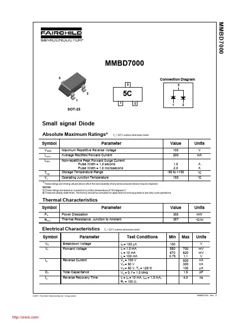

Features• LowOn-Resistance•Low Gate Threshold Voltage•Low Input Capacitance•Fast Switching Speed•Low Input/Output Leakage•ESD Protected up to 2kV•Lead Free By Design/RoHS Compliant (Note 1) •"Green" Device (Note 2)•Qualified to AEC-Q101 standards for High Reliability Mechanical Data• Case:SOT523•Case Material: Molded Plastic, “Green” Molding Compound.UL Flammability Classification Rating 94V-0•Moisture Sensitivity: Level 1 per J-STD-020• Terminals:Finish⎯ Matte Tin annealed over Alloy 42 leadframe. Solderable per MIL-STD-202, Method 208 •Terminal Connections: See Diagram•Weight: 0.002 grams (approximate)Ordering Information(Note 3)Part Number Qualification Case PackagingDMG1012T-7 Commercial SOT523 3000/Tape & ReelDMG1012TQ-7 Automotive SOT523 3000/Tape & ReelNotes: 1. No purposefully added lead.2. Diodes Inc.’s “Green” policy can be found on our website at .3. For packaging details, go to our website at .Marking InformationDate Code KeyYear2009201020112012201320142015Code W X Y Z A B C Month Jan Feb Mar Apr May Jun Jul Aug Sep Oct Nov DecCode 1 2 3 4 5 6 7 8 9 O N DSOT523Top View Equivalent Circuit Top View ESD PROTECTED TO 2kVNA1 = Product Type Marking CodeYM = Date Code MarkingY = Year (ex: W = 2009)M = Month (ex: 9 = September)NA1YMMaximum Ratings @T A = 25°C unless otherwise specifiedCharacteristic Symbol Value UnitsDrain-Source Voltage V DSS 20 V Gate-Source Voltage V GSS±6 V Continuous Drain Current (Note 4) SteadyState T A = 25°C T A = 85°CI D0.63 0.45 A Pulsed Drain Current I DM6 AThermal Characteristics @T A = 25°C unless otherwise specifiedCharacteristic Symbol Value UnitsTotal Power Dissipation (Note 4) P D0.28 W Thermal Resistance, Junction to Ambient R θJA 452 °C/W Operating and Storage Temperature Range T J, T STG -55 to +150 °CElectrical Characteristics @T A = 25°C unless otherwise specifiedCharacteristicSymbol Min Typ Max Unit Test ConditionOFF CHARACTERISTICS (Note 5) Drain-Source Breakdown VoltageBV DSS 20 - - V V GS = 0V, I D = 250μA Zero Gate Voltage Drain Current T J = 25°C I DSS - - 100 nA V DS = 20V, V GS = 0V Gate-Source LeakageI GSS - - ±1.0 μA V GS = ±4.5V, V DS = 0V ON CHARACTERISTICS (Note 5) Gate Threshold VoltageV GS(th) 0.5 - 1.0 V V DS = V GS , I D = 250μAStatic Drain-Source On-Resistance R DS (ON) - 0.3 0.4 Ω V GS = 4.5V, I D = 600mA0.4 0.5 V GS = 2.5V, I D = 500mA0.5 0.7 V GS = 1.8V, I D = 350mAForward Transfer Admittance |Y fs | - 1.4 - S V DS = 10V, I D = 400mA Diode Forward Voltage (Note 5) V SD 0.7 1.2 V V GS = 0V, I S = 150mA DYNAMIC CHARACTERISTICS Input Capacitance C iss - 60.67 - pFV DS =16V, V GS = 0V, f = 1.0MHzOutput CapacitanceC oss - 9.68 - pFReverse Transfer Capacitance C rss - 5.37 - pF Total Gate Charge Q g - 736.6 - pCV GS = 4.5V, V DS = 10V,I D = 250mAGate-Source Charge Q gs - 93.6 - pCGate-Drain Charge Q gd - 116.6 - pCTurn-On Delay Time t D(on) - 5.1 - nsV DD = 10V, V GS = 4.5V, R L = 47Ω, R G = 10Ω,I D = 200mATurn-On Rise Time t r - 7.4 - nsTurn-Off Delay Time t D(off) - 26.7 - nsTurn-Off Fall Timet f- 12.3 - nsNotes: 4. Device mounted on FR-4 PCB.5. Short duration pulse test used to minimize self-heating effect.Fig. 1 Typical Output CharacteristicsV , DRAIN-SOURCE VOLTAGE (V)DS I , D R A I N C U R R E N T (A )D00.30.60.91.21.5Fig. 2 Typical Transfer CharacteristicsV , GATE SOURCE VOLTAGE (V)GS I , D R A I N C U R R E N T (A )D00.10.20.30.40.50.60.70.800.30.60.9 1.21.5Fig. 3 Typical On-Resistance vs. Drain Current and Gate VoltageI , DRAIN-SOURCE CURRENT (A)D R , D R A I N -S O U R CE O N -R E S I S T A N C E ()D S (O N )ΩI , DRAIN CURRENT (A)Fig. 4 Typical Drain-Source On-Resistancevs. Drain Current and TemperatureD R , D R A I N -S O U R CE O N -R E S I S T A N C E ()D S (O N )ΩFig. 5 On-Resistance Variation with T emperatureT , JUNCTION TEMPERATURE (°C)J R , D R A I N -S O U R C E O N -R E S I S T A N C E (N O R M A L I Z E D )D S (O N )00.20.40.60.8Fig. 6 On-Resistance Variation with Temperature-50-250255075100125150T , JUNCTION TEMPERATURE (°C)J R , D R A I N -S O U R C E O N -R E S I S T A N C E ()D S (O N )ΩV , G A T E T H R E S H O L D V O L T A G E (V )G S (T H )Fig. 7 Gate Threshold Variation vs. Ambient Temperature T , AMBIENT TEMPERATURE (°C)AV , SOURCE-DRAIN VOLTAGE (V)SD Fig. 8 Diode Forward Voltage vs. CurrentI , S O U R C E C U R R E N T (A )SFig. 9 Typical Capacitance V , DRAIN-SOURCE VOLTAGE (V)DS C , C A P A C I T A N C E (p F )Fig. 10 Typical Drain-Source Leakage Currentvs. Drain-Source VoltageV , DRAIN-SOURCE VOLTAGE (V)DS I , D R A I N -S O U R C E L E A K A G E C U R R E N T (n A )D S S t , PULSE DURATION TIME (s)10.000010.00010.0010.010.11101001,000r (t ), T R A N S I E N T T H E R M A L R E S I S T A N C EPackage Outline DimensionsSuggested Pad LayoutSOT523Dim Min Max Typ A 0.15 0.30 0.22 B 0.75 0.85 0.80 C 1.45 1.75 1.60 D ⎯ ⎯ 0.50 G 0.90 1.10 1.00 H 1.50 1.70 1.60 J 0.00 0.10 0.05 K 0.60 0.80 0.75 L 0.10 0.30 0.22 M 0.10 0.20 0.12 N 0.45 0.65 0.50α0° 8° ⎯ All Dimensions in mmDimensions Value (in mm)Z 1.8 X 0.4 Y 0.51 C1.3 E0.7X EYCZIMPORTANT NOTICEDIODES INCORPORATED MAKES NO WARRANTY OF ANY KIND, EXPRESS OR IMPLIED, WITH REGARDS TO THIS DOCUMENT, INCLUDING, BUT NOT LIMITED TO, THE IMPLIED WARRANTIES OF MERCHANTABILITY AND FITNESS FOR A PARTICULAR PURPOSE (AND THEIR EQUIVALENTS UNDER THE LAWS OF ANY JURISDICTION).Diodes Incorporated and its subsidiaries reserve the right to make modifications, enhancements, improvements, corrections or other changes without further notice to this document and any product described herein. Diodes Incorporated does not assume any liability arising out of the application or use of this document or any product described herein; neither does Diodes Incorporated convey any license under its patent or trademark rights, nor the rights of others. Any Customer or user of this document or products described herein in such applications shall assume all risks of such use and will agree to hold Diodes Incorporated and all the companies whose products are represented on Diodes Incorporated website, harmless against all damages.Diodes Incorporated does not warrant or accept any liability whatsoever in respect of any products purchased through unauthorized sales channel. Should Customers purchase or use Diodes Incorporated products for any unintended or unauthorized application, Customers shall indemnify and hold Diodes Incorporated and its representatives harmless against all claims, damages, expenses, and attorney fees arising out of, directly or indirectly, any claim of personal injury or death associated with such unintended or unauthorized application.Products described herein may be covered by one or more United States, international or foreign patents pending. Product names and markings noted herein may also be covered by one or more United States, international or foreign trademarks.LIFE SUPPORTDiodes Incorporated products are specifically not authorized for use as critical components in life support devices or systems without the express written approval of the Chief Executive Officer of Diodes Incorporated. As used herein:A. Life support devices or systems are devices or systems which:1. are intended to implant into the body, or2. support or sustain life and whose failure to perform when properly used in accordance with instructions for use provided in thelabeling can be reasonably expected to result in significant injury to the user.B. A critical component is any component in a life support device or system whose failure to perform can be reasonably expected to cause thefailure of the life support device or to affect its safety or effectiveness.Customers represent that they have all necessary expertise in the safety and regulatory ramifications of their life support devices or systems, and acknowledge and agree that they are solely responsible for all legal, regulatory and safety-related requirements concerning their products and any use of Diodes Incorporated products in such safety-critical, life support devices or systems, notwithstanding any devices- or systems-related information or support that may be provided by Diodes Incorporated. Further, Customers must fully indemnify Diodes Incorporated and its representatives against any damages arising out of the use of Diodes Incorporated products in such safety-critical, life support devices or systems.Copyright © 2012, Diodes Incorporated分销商库存信息: DIODESDMG1012T-7。
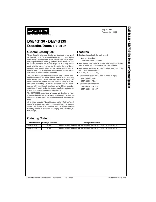
© 2000 Fairchild Semiconductor Corporation DS006466August 1986Revised April 2000DM74S138 • DM74S139 Decoder/DemultiplexerDM74S138 • DM74S139Decoder/DemultiplexerGeneral DescriptionThese Schottky-clamped circuits are designed to be used in high-performance memory-decoding or data-routing applications, requiring very short propagation delay times.In high-performance memory systems these decoders can be used to minimize the effects of system decoding. When used with high-speed memories, the delay times of these decoders are usually less than the typical access time of the memory. This means that the effective system delay introduced by the decoder is negligible.The DM74S138 decodes one-of-eight lines, based upon the conditions at the three binary select inputs and the three enable inputs. Two active-LOW and one active-HIGH enable inputs reduce the need for external gates or invert-ers when expanding. A 24-line decoder can be imple-mented with no external inverters, and a 32-line decoder requires only one inverter. An enable input can be used as a data input for demultiplexing applications.The DM74S139 comprises two separate two-line-to-four-line decoders in a single package. The active-LOW enable input can be used as a data line in demultiplexing applica-tions.All of these decoders/demultiplexers feature fully buffered inputs, presenting only one normalized load to its driving circuit. All inputs are clamped with high-performance Schottky diodes to suppress line-ringing and simplify sys-tem design.Featuress Designed specifically for high speed:Memory decoders Data transmission systemss DM74S138 3-to-8-line decoders incorporates 3 enable inputs to simplify cascading and/or data reception s DM74S139 contains two fully independent 2-to-4-line decoders/demultiplexers s Schottky clamped for high performance s Typical propagation delay time (3 levels of logic)DM74S1388 ns DM74S1397.5 ns s Typical power dissipationDM74S138245 mW DM74S139300 mWOrdering Code:Order Number Package NumberPackage DescriptionDM74S138N N16E 16-Lead Plastic Dual-In-Line Package (PDIP), JEDEC MS-001, 0.300 Wide DM74S139NN16E16-Lead Plastic Dual-In-Line Package (PDIP), JEDEC MS-001, 0.300 Wide 2D M 74S 138 • D M 74S 139Connection DiagramsDM74S138DM74S139Function TablesDM74S138DM74S139* G2 = G2A + G2B H = HIGH level L = LOW levelX = don’t care (either LOW or HIGH logic level)Logic DiagramsDM74S138DM74S139Inputs OutputsEnable Select G1G2*C B A Y0Y1Y2Y3Y4Y5Y6Y7X H X X X H H H H H H H H L X X X X H H H H H H H H H L L LL L H H H H H H H H L LL HH L H H H H H H H L L H L H H L H H H H H H L L H H H H H L H H H H H L H LLH H H H L H H H H L H L H H H H H H L H H H L H H L H H H H H H L H HLH H HHHHHHHHLInputsOutputs Enable Select G B A Y0Y1Y2Y3H X X H H H H L L L L H H H L L H H L H H L H L H H L H LHHHHHLDM74S138 • DM74S139Absolute Maximum Ratings (Note 1)Note 1: The “Absolute Maximum Ratings ” are those values beyond which the safety of the device cannot be guaranteed. The device should not be operated at these limits. The parametric values defined in the Electrical Characteristics tables are not guaranteed at the absolute maximum ratings.The “Recommended Operating Conditions ” table will define the conditions for actual device operation.Recommended Operating ConditionsElectrical Characteristicsover recommended operating free air temperature (unless otherwise noted)Note 2: All typicals are at V CC = 5V, T A = 25°C.Note 3: Not more than one output should be shorted at a time, and the duration should not exceed one second.Note 4: I CC is measured with all outputs enabled and OPEN.Supply Voltage 7V Input Voltage5.5VOperating Free Air Temperature Range 0° C to +70°C Storage Temperature Range−65° C to +150° CSymbol ParameterMin Nom Max Units V CC Supply Voltage4.7555.25V V IH HIGH Level Input Voltage 2V V IL LOW Level Input Voltage 0.8V I OH HIGH Level Output Current −1mA I OL LOW Level Output Current 20mA T AFree Air Operating Temperature70°CSymbol ParameterConditionsMinTyp Max Units (Note 2)V I Input Clamp Voltage V CC = Min, I I = −18 mA −1.2V V OH HIGH Level V CC = Min, I OH = Max 2.73.4V Output Voltage V IL = Max, V IH = Min V OL LOW Level V CC = Min, I OL = Max 0.5V Output VoltageV IH = Min, V IL = Max I I Input Current @ Max Input Voltage V CC = Max, V I = 5.5V 1mA I IH HIGH Level Input Current V CC = Max, V I = 2.7V 50µA I IL LOW Level Input Current V CC = Max, V I = 0.5V −2mA I OS Short Circuit Output Current V CC = Max (Note 3)−40−100mA I CC Supply Current (DM74S138)V CC = Max (Note 4)4974mA I CCSupply Current (DM74S139)V CC = Max (Note 4)6090mA 4D M 74S 138 • D M 74S 139DM74S138 Switching Characteristicsat V CC = 5V and T A = 25°CDM74S139 Switching Characteristicsat V CC = 5V and T A = 25°CR L = 280ΩSymbol ParameterFrom (Input)Levels C L = 15 pF C L = 50 pF UnitsTo (Output)of DelayMinMax MinMax t PLH Propagation Delay Time Select to Output 279ns LOW-to-HIGH Level Output t PHL Propagation Delay Time Select to Output 210.514ns HIGH-to-LOW Level Output t PLH Propagation Delay Time Select to Output 31214ns LOW-to-HIGH Level Output t PHL Propagation Delay Time Select to Output 31215ns HIGH-to-LOW Level Output t PLH Propagation Delay Time Enable to Output 2810ns LOW-to-HIGH Level Output t PHL Propagation Delay Time Enable to Output 21114ns HIGH-to-LOW Level Output t PLH Propagation Delay Time Enable to Output 31113ns LOW-to-HIGH Level Output t PHLPropagation Delay Time Enable to Output31114ns HIGH-to-LOW Level OutputR L = 280ΩSymbol ParameterFrom (Input)Levels C L = 15 pF C L = 50 pF UnitsTo (Output)of DelayMinMax MinMax t PLH Propagation Delay Time Select to Output 27.510ns LOW-to-HIGH Level Output t PHL Propagation Delay Time Select to Output 21013ns HIGH-to-LOW Level Output t PLH Propagation Delay Time Select to Output 31213ns LOW-to-HIGH Level Output t PHL Propagation Delay Time Select to Output 31215ns HIGH-to-LOW Level Output t PLH Propagation Delay Time Enable to Output 2810ns LOW-to-HIGH Level Output t PHLPropagation Delay Time Enable to Output21013ns HIGH-to-LOW Level Output5DM74S138 • DM74S139 Decoder/DemultiplexerPhysical Dimensions inches (millimeters) unless otherwise noted16-Lead Plastic Dual-In-Line Package (PDIP), JEDEC MS-001, 0.300 WidePackage Number N16EFairchild does not assume any responsibility for use of any circuitry described, no circuit patent licenses are implied and Fairchild reserves the right at any time without notice to change said circuitry and specifications.LIFE SUPPORT POLICYFAIRCHILD ’S PRODUCTS ARE NOT AUTHORIZED FOR USE AS CRITICAL COMPONENTS IN LIFE SUPPORT DEVICES OR SYSTEMS WITHOUT THE EXPRESS WRITTEN APPROVAL OF THE PRESIDENT OF FAIRCHILD SEMICONDUCTOR CORPORATION. As used herein:1.Life support devices or systems are devices or systems which, (a) are intended for surgical implant into the body, or (b) support or sustain life, and (c) whose failure to perform when properly used in accordance with instructions for use provided in the labeling, can be rea-sonably expected to result in a significant injury to the user.2. A critical component in any component of a life support device or system whose failure to perform can be rea-sonably expected to cause the failure of the life support device or system, or to affect its safety or effectiveness.。
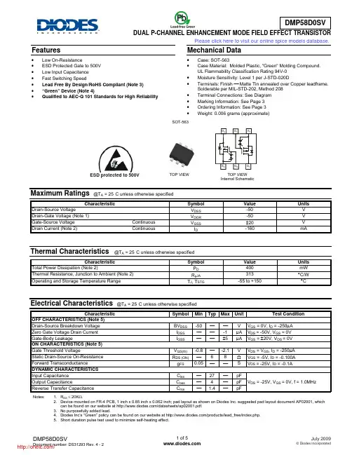
Features• Low On-Resistance • ESD Protected Gate to 500V • Low Input Capacitance • Fast Switching Speed • Lead Free By Design/RoHS Compliant (Note 3) • “Green” Device (Note 4) • Qualified to AEC-Q 101 Standards for High ReliabilityMechanical Data• Case: SOT-563• Case Material: Molded Plastic, "Green" Molding Compound.UL Flammability Classification Rating 94V-0 • Moisture Sensitivity: Level 1 per J-STD-020D • Terminals: Finish ⎯ Matte Tin annealed over Copper leadframe.Solderable per MIL-STD-202, Method 208 • Terminal Connections: See Diagram • Marking Information: See Page 3 • Ordering Information: See Page 3 • Weight: 0.006 grams (approximate)Maximum Ratings @T A = 25°C unless otherwise specifiedCharacteristic Symbol Value UnitsDrain-Source Voltage V DSS -50 V Drain-Gate Voltage (Note 1) V DGR -50 V Gate-Source Voltage Continuous V GSS ±20 V Drain Current (Note 2) Continuous I D -160 mAThermal Characteristics @T A = 25°C unless otherwise specifiedCharacteristic Symbol Value UnitsTotal Power Dissipation (Note 2) P D 400 mW Thermal Resistance, Junction to Ambient (Note 2) R θJA 313 °C/W Operating and Storage Temperature Range T J , T STG -55 to +150 °CElectrical Characteristics @T A = 25°C unless otherwise specifiedCharacteristic Symbol Min Typ Max UnitTestConditionOFF CHARACTERISTICS (Note 5) Drain-Source Breakdown Voltage BV DSS -50 ⎯ ⎯ V V GS = 0V, I D = -250μAZero Gate Voltage Drain Current I DSS ⎯ ⎯ -1 μA V DS= -50V, V GS = 0V Gate-Body Leakage I GSS ⎯ ⎯ ±5 μA V GS = ±20V, V DS = 0V ON CHARACTERISTICS (Note 5) Gate Threshold Voltage V GS(th) -0.8⎯ -2.1V V DS = V GS , I D = -250μA Static Drain-Source On-Resistance R DS (ON) ⎯ 6 8 Ω V GS = -5V, I D = -0.100A Forward Transconductance g FS 0.05⎯ ⎯ S V DS = -25V, I D = -0.1ADYNAMIC CHARACTERISTICS Input Capacitance C iss ⎯ 27 ⎯ pF V DS = -25V, V GS = 0V, f = 1.0MHzOutput Capacitance C oss ⎯ 4 ⎯pF Reverse Transfer Capacitance C rss⎯ 1.4 ⎯ pF Notes:1. R GS ≤ 20K Ω.2. Device mounted on FR-4 PCB, 1 inch x 0.85 inch x 0.062 inch; pad layout as shown on Diodes Inc. suggested pad layout document AP02001, which can be found on our website at /datasheets/ap02001.pdf.3. No purposefully added lead.4. Diodes Inc’s “Green” policy can be found on our website at /products/lead_free/index.php.5. Short duration pulse test used to minimize self-heating effect.SOT-563TOP VIEWInternal SchematicTOP VIEW ESD protected to 500V Please click here to visit our online spice models database.Fig. 1 Typical Output Characteristics-V , DRAIN-SOURCE VOLTAGE (V)DS -I , D R A I N C U R R E N T (A )DFig. 2 Typical Transfer Characteristics-V , GATE SOURCE VOLTAGE (V)GS -I , D R A I N C U R R E N T (A )DFig. 3 Typical On-Resistance vs. Drain Current and Gate Voltage-I , DRAIN CURRENT (A)D R , D R A I N -S O U R C E O N -R E S I S T A N C E ()D S (O N )Ω-I , DRAIN CURRENT (A)Fig. 4 Typical Drain-Source On-Resistancevs. Drain Current and T emperatureD R , D R A I N -S O U R CE O N -R E S I S T A N C E ()D S (O N )ΩFig. 5 On-Resistance Variation with TemperatureT , JUNCTION TEMPERATURE (°C)J R , D R A I N -T O -S O U R C E R E S I S T A N C E (N O R M A L I Z E D )D S (O N )Fig. 6 Typical Capacitance-V , DRAIN-SOURCE VOLTAGE (V)DS C , C A P A C I T A N C E (p F )Fig. 7 Gate Threshold Variation vs. Ambient T emperatureT , AMBIENT TEMPERATURE (°C)A -V , G A T E T H R E S H O L D V O L T A G E (V )G S (T H )0.0010.010.1-V , SOURCE-DRAIN VOLTAGE (V)SD -I , S O U R C E C U R R E N T (A )S Fig. 8 Diode Forward Voltage vs. CurrentFig. 9 Transient Thermal Response0.000010.00010.0010.010.11101001,000t , PULSE DURATION TIME (s)1r (t ), T R A N S I E N T T H E R M A L R E S I S T A N C EOrdering Information (Note 6)Part Number Case Packaging DMP58D0SV -7SOT-563 3000/Tape & ReelNotes: 6. For packaging details, go to our website at /datasheets/ap02007.pdf.Marking Information (Note 7)Date Code KeyYear 2007 2008 2009 2010 2011 2012 2013 2014 2015 Code U V W X Y Z A B CMonth Jan Feb Mar Apr May Jun Jul Aug Sep Oct Nov Dec Code 1 2 3 4 5 6 7 8 9 O N DNotes: 7. Package is non-polarized. Parts may be on reel in orientation illustrated, 180° rotated, or mixed (both ways).MPA = Product Type Marking CodeYM = Date Code MarkingY = Year (ex: U = 2007)M = Month (ex: 9 = September)MPA YMPackage Outline DimensionsSuggested Pad LayoutSOT-563Dim Min Max Typ A 0.15 0.30 0.20 B 1.10 1.25 1.20 C 1.55 1.70 1.60 D - - 0.50 G 0.90 1.10 1.00 H 1.50 1.70 1.60 K 0.55 0.60 0.60 L 0.100.30 0.20 M 0.10 0.18 0.11 All Dimensions in mmDimensions Value (in mm)Z 2.2 G 1.2 X 0.375 Y 0.5 C1 1.7 C2 0.5XZYC1C2C2GIMPORTANT NOTICEDIODES INCORPORATED MAKES NO WARRANTY OF ANY KIND, EXPRESS OR IMPLIED, WITH REGARDS TO THIS DOCUMENT, INCLUDING, BUT NOT LIMITED TO, THE IMPLIED WARRANTIES OF MERCHANTABILITY AND FITNESS FOR A PARTICULAR PURPOSE (AND THEIR EQUIVALENTS UNDER THE LAWS OF ANY JURISDICTION).Diodes Incorporated and its subsidiaries reserve the right to make modifications, enhancements, improvements, corrections or other changes without further notice to this document and any product described herein. Diodes Incorporated does not assume any liability arising out of the application or use of this document or any product described herein; neither does Diodes Incorporated convey any license under its patent or trademark rights, nor the rights of others. Any Customer or user of this document or products described herein in such applications shall assume all risks of such use and will agree to hold Diodes Incorporated and all the companies whose products are represented on Diodes Incorporated website, harmless against all damages.Diodes Incorporated does not warrant or accept any liability whatsoever in respect of any products purchased through unauthorized sales channel. Should Customers purchase or use Diodes Incorporated products for any unintended or unauthorized application, Customers shall indemnify and hold Diodes Incorporated and its representatives harmless against all claims, damages, expenses, and attorney fees arising out of, directly or indirectly, any claim of personal injury or death associated with such unintended or unauthorized application.Products described herein may be covered by one or more United States, international or foreign patents pending. Product names and markings noted herein may also be covered by one or more United States, international or foreign trademarks.LIFE SUPPORTDiodes Incorporated products are specifically not authorized for use as critical components in life support devices or systems without the express written approval of the Chief Executive Officer of Diodes Incorporated. As used herein:A. Life support devices or systems are devices or systems which:1. are intended to implant into the body, or2. support or sustain life and whose failure to perform when properly used in accordance with instructions for use provided in thelabeling can be reasonably expected to result in significant injury to the user.B. A critical component is any component in a life support device or system whose failure to perform can be reasonably expected to cause the failure of the life support device or to affect its safety or effectiveness.Customers represent that they have all necessary expertise in the safety and regulatory ramifications of their life support devices or systems, and acknowledge and agree that they are solely responsible for all legal, regulatory and safety-related requirements concerning their products and any use of Diodes Incorporated products in such safety-critical, life support devices or systems, notwithstanding any devices- or systems-related information or support that may be provided by Diodes Incorporated. Further, Customers must fully indemnify Diodes Incorporated and its representatives against any damages arising out of the use of Diodes Incorporated products in such safety-critical, life support devices or systems.Copyright © 2009, Diodes Incorporated分销商库存信息: DIODESDMP58D0SV-7。