DS1391中文资料
- 格式:pdf
- 大小:393.25 KB
- 文档页数:25
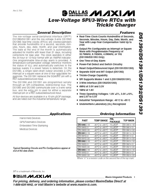
General DescriptionThe low-voltage serial-peripheral interface (SPI™)DS1390/DS1391 and the low-voltage 3-wire DS1392/DS1393 real-time clocks (RTCs) are clocks/calendars that provide hundredths of a second, seconds, min-utes, hours, day, date, month, and year information.The date at the end of the month is automatically adjusted for months with fewer than 31 days, including corrections for leap year. The clock operates in either the 24-hour or 12-hour format with an AM/PM indicator.One programmable time-of-day alarm is provided. A temperature-compensated voltage reference monitors the status of V CC and automatically disables the bus interface and switches to the backup supply if a power failure is detected. On the DS1390, a single open-drain output provides a CPU interrupt or a square wave at one of four selectable frequencies. The DS1391replaces the SQW/INT pin with a RST output/debounced input.The DS1390 and DS1391 are programmed serially through an SPI-compatible, bidirectional bus. The DS1392 and DS1393 communicate over a 3-wire serial bus, and the extra pin is used for either a separate interrupt pin or a RST output/debounced input.All four devices are available in a 10-pin µSOP package,and are rated over the industrial temperature range.ApplicationsHand-Held Devices GPS/Telematics Devices Embedded Time Stamping Medical DevicesFeatures♦Real-Time Clock Counts Hundredths of Seconds,Seconds, Minutes, Hours, Day, Date, Month, and Year with Leap-Year Compensation Valid Up to 2100♦Output Pin Configurable as Interrupt or Square Wave with Programmable Frequency of 32.768kHz, 8.192kHz, 4.096kHz, or 1Hz (DS1390/DS1393 Only)♦One Time-of-Day Alarm♦Power-Fail Detect and Switch Circuitry♦Reset Output/Debounced Input (DS1391/DS1393)♦Separate SQW and INT Output (DS1392)♦Trickle-Charge Capability♦SPI Supports Modes 1 and 3 (DS1390/DS1391)♦3-Wire Interface (DS1392/DS1393)♦4MHz at 3.0V and 3.3V ♦1MHz at 1.8V♦Three Operating Voltages: 1.8V ±5%, 3.0V ±10%,and 2.97 to 5.5V ♦Industrial Temperature Range: -40°C to +85°C ♦Underwriters Laboratory (UL) RecognizedDS1390/DS1391/DS1392/DS1393Low-Voltage SPI/3-Wire RTCs withTrickle Charger______________________________________________Maxim Integrated Products1Ordering InformationRev 1; 1/07For pricing, delivery, and ordering information,please contact Maxim/Dallas Direct!at 1-888-629-4642, or visit Maxim’s website at .Typical Operating Circuits and Pin Configurations appear at end of the data sheet.temperature range.+Denotes lead-free package.†A “+” anywhere on the top mark denotes a lead-free/RoHS-compliant package.rr = Revision code on second line of top mark.SPI is a trademark of Motorola, Inc.D S 1390/D S 1391/D S 1392/D S 1393Low-Voltage SPI/3-Wire RTCs with Trickle ChargerABSOLUTE MAXIMUM RATINGSRECOMMENDED DC OPERATING CONDITIONS(V CC = V CC(MIN)to V CC(MAX), T A = -40°C to +85°C, unless otherwise noted. Typical values are at nominal supply voltage and T A = +25°C,Stresses beyond those listed under “Absolute Maximum Ratings” may cause permanent damage to the device. These are stress ratings only, and functional operation of the device at these or any other conditions beyond those indicated in the operational sections of the specifications is not implied. Exposure to absolute maximum rating conditions for extended periods may affect device reliability.Voltage Range on V CC Pin Relative to Ground.....-0.3V to +6.0V Voltage Range on Inputs Relativeto Ground...............................................-0.3V to (V CC + 0.3V)Operating Temperature Range ...........................-40°C to +85°CStorage Temperature Range.............................-55°C to +125°C Soldering Temperature.......................................See IPC/JEDECJ-STD-020A SpecificationDS1390/DS1391/DS1392/DS1393Low-Voltage SPI/3-Wire RTCs withTrickle ChargerRECOMMENDED DC OPERATING CONDITIONS (continued)(V CC = V CC(MIN)to V CC(MAX), T A = -40°C to +85°C, unless otherwise noted. Typical values are at nominal supply voltage and T A = +25°C,D S 1390/D S 1391/D S 1392/D S 1393Low-Voltage SPI/3-Wire RTCs with Trickle Charger 4_____________________________________________________________________Figure 1. Timing Diagram—SPI Read TransferFigure 2. Timing Diagram—SPI Write TransferDS1390/DS1391/DS1392/DS1393Low-Voltage SPI/3-Wire RTCs withTrickle Charger_____________________________________________________________________5AC ELECTRICAL CHARACTERISTICSD S 1390/D S 1391/D S 1392/D S 1393Low-Voltage SPI/3-Wire RTCs with Trickle Charger 6_____________________________________________________________________Figure 3. Timing Diagram—3-Wire Read TransferFigure 4. Timing Diagram—3-Wire Write TransferDS1390/DS1391/DS1392/DS1393Low-Voltage SPI/3-Wire RTCs withTrickle Charger_____________________________________________________________________7Figure 5. Power-Up/Down TimingFigure 6. Pushbutton Reset TimingPOWER-UP/POWER-DOWN CHARACTERISTICS(T A = -40°C to +85°C) (Figures 5, 6)D S 1390/D S 1391/D S 1392/D S 1393Low-Voltage SPI/3-Wire RTCs with Trickle Charger 8_____________________________________________________________________CAPACITANCEUnder no circumstances are negative undershoots, of any amplitude, allowed when the device is in write protection.Note 1:Limits at -40°C are guaranteed by design and not production tested.Note 2:All voltages are referenced to ground.Note 3:The use of the 250Ωtrickle-charge resistor is not allowed at V CC > 3.63V and should not be enabled. Use of the diode is not recommended for V CC < 3.0V.Note 4:Measured at V CC = typ, V BACKUP = 0V, register 0Fh = A5h.Note 5:Measured at V CC = typ, V BACKUP = 0V, register 0Fh = A6h.Note 6:Measured at V CC = typ, V BACKUP = 0V, register 0Fh = A7h.Note 7:SCLK, DIN, CS on DS1390/DS1391; SCLK, and CE on DS1392/DS1393.Note 8:DOUT, SQW/INT (DS1390/DS1393), SQW, and INT (DS1392).Note 9:The RST pin has an internal 50k Ω(typ) pullup resistor to V CC .Note 10: I CCA —SCLK clocking at max frequency = 4MHz for 3V and 3.3V versions; 1MHz for 1.8V version; RST (DS1391/DS1393)inactive. Outputs are open.Note 11:Specified with bus inactive.Note 12:Measured with a 32.768kHz crystal attached to X1 and X2. Typical values measured at +25°C and 3.0V BACKUP .Note 13:With 50pF load.Note 14:Measured at V IH = 0.7 x V DD or V IL = 0.2 x V DD , 10ns rise/fall times.Note 15:Measured at V OH = 0.7 x V DD or V OL = 0.2 x V DD . Measured from the 50% point of SCLK to the V OH minimum of SDO.Note 16:The parameter t OSF is the time that the oscillator must be stopped for the OSF flag to be set over the voltage range of 0 ≥V CC ≥V CC(MAX)and 1.3V ≤V BACKUP ≤5.5V.Note 17:This delay applies only if the oscillator is enabled and running. If the EOSC bit is 1, the startup time of the oscillator is added to this delay.DS1390/DS1391/DS1392/DS1393Low-Voltage SPI/3-Wire RTCs withTrickle Charger_____________________________________________________________________9Typical Operating Characteristics(V CC = +3.3V, T A = +25°C, unless otherwise noted.)I BACKUP vs. V BACKUP , BBSQ1 = 0V BACKUP (V)S U P P L Y C U R R E N T (n A )4.5 4.94.13.3 3.72.92.52.11.73504004505005506003001.3 5.3I BACKUP vs. V BACKUP , BBSQ1 = 1V BACKUP (V)S U P P L Y C U R R E N T (n A )5.34.94.1 4.52.1 2.5 2.9 3.3 3.71.735040045050055060065070075080085090095010003001.3I BACKUP vs. TEMPERATUREV BACKUP = 3.0VTEMPERATURE (°C)S U P P L Y C U R R E N T (n A )80604020-20300400350450500550600250-40OSCILLATOR FREQUENCY vs. SUPPLY VOLTAGED S 1390 t o c 04SUPPLY (V)F R E Q U E N C Y (H z )5.34.84.33.83.32.82.31.832767.8532767.9032767.9532768.0032767.801.3D S 1390/D S 1391/D S 1392/D S 1393Low-Voltage SPI/3-Wire RTCs with Trickle ChargerDetailed Description The DS1390/DS1391/DS1392/DS1393 RTCs are low-power clocks/calendars with alarms. Address and data are transferred serially through a 4-wire SPI interface for the DS1390 and DS1391 and through a 3-wire interface for the DS1392 and DS1393. The DS1390/DS1391 oper-ate as a slave device on the SPI serial bus. The DS1392/DS1393 operate using a 3-wire synchronous serial bus. Access is obtained by selecting the part by the CS pin (CE on DS1392/DS1393) and clocking data into/out of the part using the SCLK and DIN/DOUT pins (I/O on DS1392/DS1393). Multiple-byte transfers are supported within one CS low period (see the SPI Serial-Data Bus section). The clocks/calendars provide hun-dredths of seconds, seconds, minutes, hours, day, date,month, and year information. The alarm functions are performed off all timekeeping registers, allowing the userto set high resolution alarms. The date at the end of the month is automatically adjusted for months with fewerthan 31 days, including corrections for leap year. The clocks operate in either the 24-hour or 12-hour formatwith an AM/PM indicator. All four devices have a built-in temperature-compensated voltage reference that detects power failures and automatically switches to the battery supply. Additionally, the devices can providetrickle charging of the backup voltage source, with selectable charging resistance and diode voltage drops. DS1390/DS1391/DS1392/DS1393Low-Voltage SPI/3-Wire RTCs withTrickle ChargerFunctional DiagramD S 1390/D S 1391/D S 1392/D S 1393Power ControlThe power-control function is provided by a precise,temperature-compensated voltage reference and a comparator circuit that monitors the V CC level. The device is fully accessible and data can be written and read when V CC is greater than V PF . However, when V CC falls below V PF , the internal clock registers are blocked from any access. If V PF is less than V BACKUP ,the device power is switched from V CC to V BACKUP when V CC drops below V PF . If V PF is greater than V BACKUP , the device power is switched from V CC to V BACKUP when V CC drops below V BACKUP .Timekeeping operation and register data are main-tained from the V BACKUP source until V CC is returned to nominal levels (Table 1). After V CC returns above V PF ,read and write access is allowed after RST goes high (Figure 5).Oscillator CircuitAll four devices use an external 32.768kHz crystal. The oscillator circuit does not require any external resistors or capacitors to operate. Table 2 specifies several crys-tal parameters for the external crystal, and Figure 7shows a functional schematic of the oscillator circuit. If a crystal is used with the specified characteristics, the startup time is usually less than one second.Clock AccuracyThe accuracy of the clock is dependent upon the accu-racy of the crystal and the accuracy of the match between the capacitive load of the oscillator circuit and the capacitive load for which the crystal was trimmed.Additional error is added by crystal frequency drift caused by temperature shifts. External circuit noise coupled into the oscillator circuit can result in the clock running fast. Figure 8 shows a typical PC board layout for isolation of the crystal and oscillator from noise.Refer to Application Note 58: Crystal Considerations with Dallas Real-Time Clocks for detailed information.Low-Voltage SPI/3-Wire RTCs with Trickle ChargerFigure 7. Oscillator Circuit Showing Internal Bias Network Figure 8. Layout ExampleAddress Map Table3 shows the address map for the DS1390–DS1393 RTC and RAM registers. The RTC registers are located in address locations 00h to 0Fh in read mode, and 80h to 8Fh in write mode. During a multibyte access, when the address pointer reaches 0Fh, it wraps around to location 00h. On the falling edge of the CS pin (DS1390/DS1391) or the rising edge of CE (DS1392/DS1393), the current time is transferred to a second set of registers. The time information is readfrom these secondary registers, while the clock may continue to run. This eliminates the need to re-read the registers if the main registers update during a read. Toavoid rollover issues when writing to the time and date registers, all registers should be written before the hun-dredths-of-seconds registers reaches 99 (BCD).DS1390/DS1391/DS1392/DS1393Low-Voltage SPI/3-Wire RTCs withTrickle ChargerD S 1390/D S 1391/D S 1392/D S 1393Hundredths-of-SecondsGeneratorThe hundredths-of-seconds generator circuit shown in the functional diagram is a state machine that divides the incoming frequency (4096Hz) by 41 for 24 cycles and 40 for one cycle. This produces a 100Hz output that is slightly off during the short term, and is exactly correct every 250ms. The divide ratio is given by:Ratio = [41 x 24 + 40 x 1] / 25 = 40.96Thus, the long-term average frequency output is exactly the desired 100Hz.Clock and CalendarThe time and calendar information is obtained by read-ing the appropriate register bytes. See Table 3for the RTC registers. The time and calendar are set or initial-ized by writing the appropriate register bytes. The con-tents of the time and calendar registers are in the binary-coded decimal (BCD) format. The day-of-week register increments at midnight. Values that correspond to the day-of-week are user-defined but must be sequential (i.e., if 1 equals Sunday, then 2 equals Monday, and so on). Illogical time and date entries result in undefined operation. The DS1390–DS1393 can run in either 12-hour or 24-hour mode. Bit 6 of the hoursregister is defined as the 12- or 24-hour mode-select bit. When high, the 12-hour mode is selected. In the 12-hour mode, bit 5 is the AM /PM bit with logic high being PM. In the 24-hour mode, bit 5 is the second 10-hour bit (20 to 23 hours). Changing the 12/24-hour mode-select bit requires that the hours data be re-entered,including the alarm register (if used). The century bit (bit 7 of the month register) is toggled when the years register overflows from 99 to 00.AlarmsAll four devices contain one time-of-day/date alarm.Writing to registers 88h through 8Ch sets the alarm.The alarm can be programmed (by the alarm enable and INTCN bits of the control register) to activate the SQW/INT or INT output on an alarm-match condition.The alarm can activate the SQW/INT or INT output while the device is running from V BACKUP if BBSQI is enabled. Bit 7 of each of the time-of-day/date alarm registers are mask bits (Table 4). When all the mask bits for each alarm are logic 0, an alarm only occurs when the values in the timekeeping registers 00h to 06h match the values stored in the time-of-day/date alarm registers. The alarms can also be programmed to repeat every second, minute, hour, day, or date. Table 4 shows the possible settings. Configurations not listed in the table result in illogical operation.Low-Voltage SPI/3-Wire RTCs with Trickle ChargerThe DY/DT bits (bit 6 of the alarm day/date registers) control whether the alarm value stored in bits 0 to 5 of that register reflects the day of the week or the date of the month. If DY/DT is written to logic 0, the alarm is the result of a match with date of the month. If DY/DT is written to a logic 1, the alarm is the result of a match with day of the week.When the RTC register values match alarm register set-tings, the alarm-flag (AF) bit is set to logic 1. If the alarm-interrupt enable (AIE) is also set to logic 1 and the INTCN bit is set to logic 1, the alarm condition acti-vates the SQW/INT signal.Since the contents of register 08h are expected to nor-mally contain a match value of 00–99 decimal, the codes F[0–9], and FF have been used to tell the part to mask the tenths or hundredths of seconds accordingly.Power-Up/Down, Reset, andPushbutton Reset FunctionsA precision temperature-compensated reference and comparator circuit monitors the status of V CC. When anout-of-tolerance condition occurs, an internal power-failsignal is generated that blocks read/write access to the device and forces the RST pin (DS1391/DS1393 only)low. When V CC returns to an in-tolerance condition, the internal power-fail signal is held active for t RST to allowthe power supply to stabilize, and the RST(DS1391/DS1393 only) pin is held low. If the EOSC bit is set tologic 1 (to disable the oscillator in battery-backup mode), the internal power-fail signal and the RST pin iskept active for t RST plus the startup time of the oscillator.The DS1391/DS1393 provide for a pushbutton switch tobe connected to the RST output pin. When theDS1391/DS1393 are not in a reset cycle, it continuously monitors the RST signal for a low-going edge. If anedge is detected, the part debounces the switch by pulling the RST pin low and inhibits read/write access.After PB DB has expired, the part continues to monitorthe RST line. If the line is still low, it continues to monitorthe line looking for a rising edge. Upon detecting release, the part forces the RST pin low and holds it low for an additional PB DB.DS1390/DS1391/DS1392/DS1393Low-Voltage SPI/3-Wire RTCs withTrickle ChargerD S 1390/D S 1391/D S 1392/D S 1393Bit 7: Enable Oscillator (EOSC ).When set to logic 0,this bit starts the oscillator. When this bit is set to logic 1, the oscillator is stopped whenever the device is pow-ered by V BACKUP . The oscillator is always enabled when V CC is valid. This bit is enabled (logic 0) when V CC is first applied.Bit 5: Battery-Backed Square-Wave and Interrupt Enable (BBSQI).This bit when set to logic 1 enables the square wave or interrupt output when V CC is absent and the DS1390/DS1392/DS1393 are being powered by the V BACKUP pin. When BBSQI is logic 0, the SQW/INT pin (or SQW and INT pins) goes high imped-ance when V CC falls below the power-fail trip point.This bit is disabled (logic 0) when power is first applied.Bits 4 and 3: Rate Select (RS2 and RS1).These bits control the frequency of the square-wave output when the square wave has been enabled. The table below shows the square-wave frequencies that can be select-ed with the RS bits. These bits are both set to logic 1Bit 2: Interrupt Control (INTCN). This bit controls the SQW/INT signal. When the INTCN bit is set to logic 0, a square wave is output on the SQW/INT pin. The oscilla-tor must also be enabled for the square wave to be out-put. When the INTCN bit is set to logic 1, a match between the timekeeping registers and either of the alarm registers then activates the SQW/INT (provided the alarm is also enabled). The corresponding alarm flag is always set, regardless of the state of the INTCN bit. The INTCN bit is set to logic 0 when power is first applied.Bit 0: Alarm Interrupt Enable (AIE).When set to logic 1, this bit permits the alarm flag (AF) bit in the status register to assert SQW/INT (when INTCN = 1). When the AIE bit is set to logic 0 or INTCN is set to logic 0,the AF bit does not initiate the SQW/INT signal. The AIE bit is disabled (logic 0) when power is first applied.Low-Voltage SPI/3-Wire RTCs with Trickle Charger Control Register (0D/8Dh) (DS1390/DS1393 Only)Control Register (0D/8Dh) (DS1391 Only)Special-Purpose RegistersThe DS1390–DS1393 have three additional registers (control, status, and trickle charger) that control the RTC, alarms, square-wave output, and trickle charger.pose, battery-backed, nonvolatile SRAM bits in the DS1391.Bit 7: Oscillator Stop Flag (OSF).A logic 1 in this bit indicates that the oscillator has stopped or was stopped for some time and may be used to judge the validity of the clock and calendar data. This bit is edge-triggered and is set to logic 1 when the internal circuitry senses the oscillator has transitioned from a normal run state to a STOP condition. The following are examples of conditions that can cause the OSF bit to be set:1)The first time power is applied.2)The voltage present on V CC and V BACKUP is insufficient to support oscillation.3)The EOSC bit is turned off.4)External influences on the crystal (i.e., noise,leakage, etc.).This bit remains at logic 1 until written to logic 0. This bit can only be written to logic 0. Attempting to write OSF to logic 1 leaves the value unchanged.Bit 6: Alarm Flag (AF).A logic 1 in the AF bit indicates that the time matched the alarm registers. If the AIE bitthe SQW pin-enable bit in the DS1392. This bit powersDS1390/DS1391/DS1392/DS1393Low-Voltage SPI/3-Wire RTCs withTrickle ChargerD S 1390/D S 1391/D S 1392/D S 1393The user determines diode and resistor selection according to the maximum current desired for battery or super cap charging. The maximum charging current can be calculated as illustrated in the following exam-ple. Assume that a system power supply of 3.3V is applied to V CC and a super cap is connected to V BACKUP . Also, assume that the trickle charger has been enabled with a diode and resistor R2 betweenV CC and V BACKUP . The maximum current I MAX would therefore be calculated as follows:I MAX = (3.3V - diode drop) / R2 ≈(3.3V - 0.7V) /2k Ω≈1.3mAAs the super cap changes, the voltage drop between V CC and V BACKUP decreases and therefore the charge current decreases.Low-Voltage SPI/3-Wire RTCs with Trickle ChargerFigure 9. DS1390/DS1391 Programmable Trickle ChargerSPI Serial-Data Bus The DS1390/DS1391 provide a 4-wire SPI serial-data bus to communicate in systems with an SPI host con-troller. Both devices support single-byte and multiple-byte data transfers for maximum flexibility. The DIN and DOUT pins are the serial-data input and output pins, respectively. The CS input initiates and terminates a data transfer. The SCLK pin synchronizes data move-ment between the master (microcontroller) and the slave (DS1390/DS1391) devices. The shift clock (SCLK), which is generated by the microcontroller, is active only during address and data transfer to any device on the SPI bus. Input data (DIN) is latched on the internal strobe edge and output data (DOUT) is shifted out on the shift edge (Figure 10). There is one clock for each bit transferred. Address and data bits are transferred in groups of eight.Address and data bytes are shifted MSB first into the serial-data input (DIN) and out of the serial-data output (DOUT). Any transfer requires the address of the byte to specify a write or read, followed by one or more bytes of data. Data is transferred out of the DOUT pin for a read operation and into the DIN for a write opera-tion (Figures 11 and 12).The address byte is always the first byte entered afterCS is driven low. The most significant bit (W/R) of thisbyte determines if a read or write takes place. If W/R is0, one or more read cycles occur. If W/R is 1, one ormore write cycles occur.Data transfers can occur one byte at a time or in multi-ple-byte burst mode. After CS is driven low, an addressis written to the DS1390/DS1391. After the address, oneor more data bytes can be written or read. For a single-byte transfer, one byte is read or written and then CS is driven high. For a multiple-byte transfer, however, multi-ple bytes can be read or written after the address hasbeen written. Each read or write cycle causes the RTC register address to automatically increment. Incrementing continues until the device is disabled.The address wraps to 00h after incrementing to 0Fh (during a read) and wraps to 80h after incrementing to8Fh (during a write). Note, however, that an updatedcopy of the time is only loaded into the user-accessiblecopy upon the falling edge of CS. Reading the RTC registers in a continuous loop does not show the time advancing. DS1390/DS1391/DS1392/DS1393Low-Voltage SPI/3-Wire RTCs withTrickle ChargerFigure 11. SPI Single-Byte WriteFigure 12. SPI Single-Byte ReadD S 1390/D S 1391/D S 1392/D S 1393Low-Voltage SPI/3-Wire RTCs with Trickle ChargerFigure 13. SPI Multiple-Byte Burst TransferFigure 14. 3-Wire Single-Byte ReadFigure 15. 3-Wire Single-Byte Write3-Wire Serial-Data BusThe DS1392/DS1393 provide a 3-wire serial-data bus,and support both single-byte and multiple-byte data transfers for maximum flexibility. The I/O pin is the seri-al-data input/output pin. The CE input is used to initiate and terminate a data transfer. The SCLK pin is used to synchronize data movement between the master (microcontroller) and the slave (DS1392/DS1393)devices. Input data is latched on the SCLK rising edge and output data is shifted out on the SCLK falling edge.There is one clock for each bit transferred. Address and data bits are transferred in groups of eight.Address and data bytes are shifted LSB first into the I/O pin. Data is transferred out LSB first on the I/O pin for a read operation.The address byte is always the first byte entered after CE is driven high. The MSB (W/R ) of this byte deter-mines if a read or write takes place. If W/R is 0, one or more read cycles occur. If W/R is 1, one or more write cycles occur.Data transfers can be one byte at a time or in multiple-byte burst mode. After CE is driven high, an address is written to the DS1392/DS1393. After the address, one or more data bytes can be written or read. For a single-byte transfer, one byte is read or written and then CE is driven low (Figure 14 and 15). For a multiple-byte trans-fer, however, multiple bytes can be read or written after the address has been written (Figure 16). Each read or write cycle causes the RTC register address to auto-matically increment. Incrementing continues until the device is disabled. The address wraps to 00h afterincrementing to 0Fh (during a read) and wraps to 80h after incrementing to 8Fh (during a write). Note, howev-er, that an updated copy of the time is only loaded into the user-accessible copy upon the rising edge of CE.Reading the RTC registers in a continuous loop does not show the time advancing.Chip InformationTRANSISTOR COUNT: 11,525PROCESS: CMOSSUBSTRATE CONNECTED TO GROUNDThermal InformationTheta-JA: 180°C/W Theta-JC: 41.9°C/WDS1390/DS1391/DS1392/DS1393Low-Voltage SPI/3-Wire RTCs withTrickle Charger____________________________________________________________________21Figure 16. 3-Wire Multiple-Byte Burst TransferD S 1390/D S 1391/D S 1392/D S 1393Low-Voltage SPI/3-Wire RTCs with Trickle Charger 22____________________________________________________________________Pin ConfigurationsDS1390/DS1391/DS1392/DS1393Low-Voltage SPI/3-Wire RTCs withTrickle Charger____________________________________________________________________23Typical Operating CircuitsPackage Information(The package drawing(s) in this data sheet may not reflect the most current specifications. For the latest package outline information,go to /DallasPackInfo ).D S 1390/D S 1391/D S 1392/D S 1393Low-Voltage SPI/3-Wire RTCs with Trickle Charger 24____________________________________________________________________DS1390/DS1391/DS1392/DS1393Low-Voltage SPI/3-Wire RTCs withTrickle ChargerMaxim cannot assume responsibility for use of any circuitry other than circuitry entirely embodied in a Maxim product. No circuit patent licenses are implied. Maxim reserves the right to change the circuitry and specifications without notice at any time.Maxim Integrated Products, 120 San Gabriel Drive, Sunnyvale, CA 94086 408-737-7600 ____________________25©2007 Maxim Integrated Productsis a registered trademark of Maxim Integrated Products.is a registered trademark of Dallas Semiconductor Corporation.Revision HistoryRev 0;7/04:Original data sheet release.Rev 1;1/07:Added text to the General Description section to indicate that the bus interface is disabled when the part switches to V BACKUP (page 1).Replaced Ordering Information table with lead-free packages (page 1).Added 0MHz (min) spec for SCLK frequency for SPI, 3-wire AC timing (pages 3 and 5).Added the “High Impedance” label for DOUT to Figure 1 and added DOUT trace to Figure 2 (page 4).Changed all references of V BAT to V BACKUP (pages 8 and 10).Replaced the Operation section with the Power Control section and added new Table 1 (pages 11and 12).。