MYC-AM335X核心板引脚定义说明列表
- 格式:pdf
- 大小:99.60 KB
- 文档页数:1
Board Porting\Bring up using Processor SDK RTOS for AM335xProcessor SDK RTOS component known as board library consolidates all the board-specific information so that all the modifications made when moving to a new custom platform using the SOC can be made in the source of this library.There are three different components in PRSDK that help in porting and bring up of a custom board:∙Board library updatesa.PLL Clocking and PRCMb.Pin mux Updatec.DDR Configurationd.Peripheral instances updates∙Diagnostics tests∙Boot loader updatesBoard Library Updates in Processor SDK RTOS:PLL ClockingThere are two places where the device PLL configurations are performed when using Processor SDK RTOS and CCS.Debug environment:Debug environment refers to development setup where code is debugged using JTAG emulator on the SOC. The PRSDK software relies on the GEL file that is part of the target configuration to setup the clocks and the DDR for the device. The CCS GEL file for AM335x platforms is located in the CCS package at the location ccsv7\ccs_base\emulation\boards\<boardName>For example for beagle bone black, the files can be found atccsv7\ccs_base\emulation\boards\beaglebone\gelThe GEL is the first piece of software that should be brought up on a custom board.Production environment:Production environment refers to the setup when the base application is booted from a boot media like a flash memory or host interface. In this environment, the bootloader sets performs all the SOC and board initialization and copies the application from flash memory to the device memory.The clock setup in the bootloader code can be located atpdk_am335x_x_x_x\packages\ti\starterware\bootloader\src\am335xUsers can choose to use the platform clocking similar to one of TI reference platforms or can modify them as per their application requirements. By default the PLL settings are setup for OPP_NOM settings (MPU= 600 MHz.)TI provides Clock Tree tool to allow users to simulate the clocking on the SOC. For quick reference of the multiplier and divider settings to change the PLL setting is provided in the spreadsheetAM335x_DPLL_CALCv3.xlsx.After modifying the clocking in the bootloader, users need to rebuild the bootloader using instructions provided in Processor_SDK_RTOS_BOOT_AM335x/AM437xPRCM Modules Enable:PRCM Module Enable is required to turn on the power domain and the clocking to each of the modules on the SOC. The PRCM Enable calls to enable each module are made from the functionBoard_moduleClockInit which is found in the location.pdk_am335x_1_0_9\packages\ti\board\src\bbbAM335x\bbbAM335x.cCheck every instance and peripheral required in the application platform and enable the module in the board library.For example to use three UARTs 0, 1 and 4, ensure that you have the following code as part of the board library setup:/* UART */status = PRCMModuleEnable(CHIPDB_MOD_ID_UART, 0U, 0U);status = PRCMModuleEnable(CHIPDB_MOD_ID_UART, 1U, 0U);status = PRCMModuleEnable(CHIPDB_MOD_ID_UART, 4U, 0U);Note: PRCMEnable function is defined in pdk_am335x_1_0_9\packages\ti\starterware\soc\am335x Pinmux updates in the Board library:Generating a New PinMux Configuration Using the PinMux Utility: This procedure uses the cloud-based pinmux utilityNavigate to ${PDK_INSTALL_DIR}\packages\ti\starterware\tools\pinmux_config\am335x and Load beaglebone_black_configAdd and remove peripheral instances and select the appropriate use cases required for development based on the application platform requirements and resolve all conflicts.Refer Pin_Mux_Utility_for_ARM_MPU_ProcessorsPost Processing steps:1.Change the Category filter to starterware and download the pinmux files am335x_pimnmux.hand am335x_pinmux_data.c2.At the bottom of am335x_pinmux.h change extern pinmuxBoardCfg_t gAM335xPinmuxData[];to extern pinmuxBoardCfg_t gBbbPinmuxData[];3.Change am335x_pinmux_data.c to am335x_beagleboneblack_pinmux_data.c.4.Change gAM335xPinmuxData to gBbbPinmuxData at the end of the file in file5.am335x_beagleboneblack_pinmux_data.c.Replace the existing files with the new files and rebuild the board library using the instructions in the section Rebuilding board Library in Processor SDK RTOS:Updating DDR settings:Similar to clock and PLL settings, DDR initialization is configured in the Debug environment through GEL files and in production environment using bootloader source files.TI provides AM335x_EMIF_Configuration_tips which contains a spreadsheet to enter the timing from the DDR datasheet to compute the EMIF timing number required to initialize DDR.We strongly recommend changing the value and testing using GEL files before using them in the bootloader software. For Sanity test, you can perform read/write tests using CCS Memory Browser or run the diagnostic memory read/write test that we provide in diagnostics package here:PDK_INSTALL_PATH\packages\ti\board\diag\memOnce the DDR timings have been confirmed, you can use the settings in the file:PDK_INSTALL_PATH \packages\ti\starterware\bootloader\src\am335x\sbl_am335x_platform_ddr.c Peripheral initialization:The board library is responsible for most of the SOC initialization but it also setup some board level components such as ethernet PHY and debug UART and I2C for reading board ID from EEPROM. All of the other peripheral instances and initialization needs to be done from the application level.For example for beagleboneblack, the peripheral initialization are performed from the source filepdk_am335x_1_0_9\packages\ti\board\src\bbbAM335x\bbbAM335x_lld_init.cThe debug UART instance, I2C Addresses are set using the file board_cfg.h found under:pdk_am335x_1_0_9\packages\ti\board\src\bbbAM335x\includeDefault UART instance is set to 0 in the board library. The Board initialization will configure the UART instance 0 to send binary log data to serial console using the Board_UARTInit function. If you wish to use more UART instances then we recommend linking in the UART driver in the application and using UART_open() and UART_stdioInit API calls from the application.Each peripheral driver in the Processor SDK RTOS has a SOC configuration that provides the interrupt numbers, base address, EDMA channels which can be updated using the file <peripheral>_soc.c file. This is used as default setup for initializing the driver instance. It can be overridden from the application using peripheral_getSOCInitCfg() and peripheral_setSOCInitCfg()For Example: All instances of UART for AM335x have been mapped in the filepdk_am335x_1_0_9\packages\ti\drv\uart\soc\am335x\UART_soc.cSystem integrators need to ensure that no interrupt numbers and EDMA resource conflicts exist in the SOC configuration for all drivers used in the system.To exercise three UARTs in the system, users can use the following code://Setup Debug UARTboardCfg = BOARD_INIT_PINMUX_CONFIG |BOARD_INIT_MODULE_CLOCK |BOARD_INIT_UART_STDIO;Board_init(boardCfg);// Open Additional UART Instances:/* UART SoC init configuration */UART_initConfig(false);/* Initialize the default configuration params. */UART_Params_init(&uartParams);// Open UART Instance 1uartTestInstance =1;uart1 = UART_open(uartTestInstance, &uartParams);//Open UART Instance 4uartTestInstance = 4;uart4 = UART_open(uartTestInstance, &uartParams);BoardID Detect:TI supports multiple evaluation and reference platforms for AM335x hence the hardware platforms are populated with an EEPROM which contains information that identifies the hardware and its revision. The board library and software components read the boardID and initialize the platform based on the boardID. The BoardID_detect function can be found in the source in the file bbbAM335x_info.c in the board library and board_am335x.c in the bootloader source at:<PDK_INSTALL_PATH>\packages\ti\starterware\board\am335xRebuilding board Library in Processor SDK RTOS:While Creating a new folder for the custom board is an option users can explore, TI recommends that users make there changes in existing board package using either bbbAM335x, evmAM335x oriceAM335x folder to avoid spending additional effort to modify the build files for including the customBord.Once all the update to the board library are completed, the board library can be updated using the following instructions.Instructions to rebuild board library:Setup Processor SDK build environment before following steps provided below.cd pdk_am335x_1_0_9\packagesgmake board_libFor a specific board users are required to provide the LIMIT_BOARDS argument.LIMIT_BOARDS : evmAM335x icev2AM335x iceAMIC110 bbbAM335x skAM335xFor Example for beagleboneblack, users can use the following build option:gmake board_lib LIMIT_BOARDS=bbbAM335xDiagnostics:After the board library is built, we highly recommend that you create a diagnostics package similar to one provided in board library to test different interfaces functionally during board bring up.The diagnostics package can be located at pdk_am335x_1_0_9\packages\ti\board\diag. These are simple bare-metal tests that use peripheral drivers to help functionally validate the pins and interfaces.Documentation for all available diagnostic tests is provided here:/index.php/Processor_SDK_RTOS_DIAGBootloader in Processor SDK RTOS:As part of the production flow, users are required to develop/port flashing and booting utilities so the application can be launched on the custom board with JTAG. TI provides a bootloader mechanism where the ROM bootloader loads a secondary bootloader on the onchip memory that initializes the SOC and DDR and then copies the application into DDR memory.The boot process and flashing tools have been described in detail in the following article that is part of processor SDK RTOS Software developer`s guide:/index.php/Processor_SDK_RTOS_BOOT_AM335x/AM437x#Building_the_B ootloader。
AM335XGPIO详解1、配置GPIO1的时钟CM_PER RegistersCM_PER_GPIO1_CLKCTRL该寄存器管理GPIO1时钟。
OPTFCLKEN_GPIO_1_GDBCLK 可选功能时钟控制0X0 = FCLK_DIS :可选功能的时钟被禁止0x1 = FCLK_EN :可选功能时钟使能IDLEST 模块为空闲状态0X0 =函数功能:模块功能齐全,包括OCP0x1 =反:模块进行转换:唤醒或休眠,或睡眠流产0X2 =空闲:模块处于空闲模式(仅OCP部分)。
它是功能,如果使用独立的时钟功能0x3的=禁止:禁止模块,不能访问CM_PER_L4LS_CLKSTCTRL该寄存器使能域功率状态转换。
它控制着SW监督时钟域状态ON- PER和ON- INPER状态之间的转换。
它也认为每个时钟输入1个状态位域。
CLKACTIVITY_GPIO_1_GDBCLK 该字段表示在该GPIO1_GDBCLK时钟的状态域。
0X0 = INACT :对应的时钟门控0x1 =ACT:通讯时钟有效2、配置GPIO端口功能CONTROL_MODULE Registersconf_gpmc_a0-a11 设置内部上拉和管脚传输速率:快或慢3、重启GPIO模块GPIO_SYSCONFIG 寄存器1 SOFTRESET R/W Software reset.This bit is automatically reset by the hardware. During reads, it always returns 0.0x0 = Normal mode0x1 = The module is rese软件复位。
该位由硬件自动复位。
在读取时,它总是返回0 。
0X0 =普通模式为0x1 =该模块复位4、设置GPIO方向GPIO_OE[0-31] 寄存器输出数据使能0X0 =相应的GPIO端口被配置为输出。
0x1 =相应的GPIO端口配置为输入。
电源管理芯片引脚界说之老阳三干创作
1、 VCC 电源管理芯片供电
2、 VDD 门驱动器供电电压输入或低级控制信号供电源
3、VID-4 CPU与CPU供电管理芯片VID信号连接引脚, 主要指示
芯片的输出信号, 使两个场管输出正确的工作电压.
4、RUN SD SHDN EN 分歧芯片的开始工作引脚.
5、PGOOD PG cpu内核供电电路正常工作信号输出.
6、VTTGOOD cpu外核供电正常信号输出.
7、UGATE 高端场管的控制信号.
8、LGATE 低端场管的控制信号.
9、PHASE 相电压引脚连接过压呵护端.
10、VSEN 电压检测引脚.
11、FB 电流反馈输入即检测电流输出的年夜小.
12、COMP 电流赔偿控制引脚.
13、DRIVE cpu外核场管驱动信号输出.
14、OCSET 12v供电电路过流呵护输入端.
15、BOOT 次级驱动信号器过流呵护输入端.
16、VIN cpu外核...
CC:C=circuit 暗示电路的意思, 即接入电路的电压;。
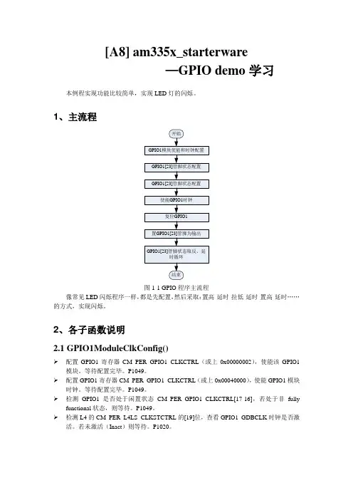
[A8] am335x_starterware—GPIO demo学习本例程实现功能比较简单,实现LED灯的闪烁。
1、主流程图1-1 GPIO程序主流程像常见LED闪烁程序一样,都是先配置,然后采取:置高-延时-拉低-延时-置高-延时……的方式,实现闪烁。
2、各子函数说明2.1 GPIO1ModuleClkConfig()配置GPIO1寄存器CM_PER_GPIO1_CLKCTRL(或上0x00000002),使能该GPIO1模块。
等待配置完毕。
P1049。
配置GPIO1寄存器CM_PER_GPIO1_CLKCTRL(或上0x00040000),使能GPIO1模块时钟。
等待配置完毕。
P1049。
检测GPIO1是否处于闲置状态CM_PER_GPIO1_CLKCTRL[17-16],若处于非fully functional状态,则等待。
P1049。
检测L4的CM_PER_L4LS_CLKSTCTRL的[19]位,查看GPIO1_GDBCLK时钟是否激活。
若未激活(Inact)则等待。
P1020。
2.2 GPIO1Pin23PinMuxSetup()GPIO1Pin23PinMuxSetup()配置GPMC_A7(GPIO1_23)引脚,配置为高速、下拉并使能。
Register=0x00000007。
p1278。
功能服用配置位为该寄存器[2:0],配置为111b,还未搞清楚。
2.3 GPIOModuleEnable()GPIOModuleEnable(GPIO_INSTANCE_ADDRESS)配置GPIO1时钟使能,GPIO_CTRL。
GPIO_CTRL[0]=0,使能GPIO1模块。
P4524。
2.4 GPIOModuleReset()GPIOModuleReset(GPIO_INSTANCE_ADDRESS)复位GPIO1各端口。
GPIO_SYSCONFIG。
GPIO_SYSCONFIG[1]=1,软件写1复位,复位GPIO1各端口。
How to use the AM335x IBIS ModelsIntroductionThe AM335x External Memory Interface is a very flexible interface which can be used with LPDDR, DDR2, DDR3, and DDR3L. There are many settings available to fine-tune the signal timing on this interface. These settings include ODT options, pullups, pulldowns, slew rate, etc. IBIS modeling can be used to fine tune the set of options for a given PCB. That said, understanding the mapping between the various IBIS models and the corresponding register configuration options is critical to doing this correctly. This article is intended to help bridge that gap so that AM335x users can properly model their memory interface and program the best options in the AM335x registers. NOTE: TI does not support timing analysis with IBIS simulations. Rather, customers are encouraged to use the IBIS models for Signal Integrity (SI) analysis. As far as the timing goes, please follow the routing guidelines and length/skew matching requirements in the Data Manual.IBIS StructureEvery pin on the device is listed with a corresponding "Selector". For example:P1 DDR_DQS0 Selector_1If you then go and look at the definition of that Selector you will find all of the available models for that given I/O cell. For example:[Model Selector] Selector_1Model_1000 INPUT,1.5V,FULLTERM, 1.00*RExt,IND,5%,DIFF_VREF_FULLTERM_8MA_5PER_1P5 Model_1001 INPUT,1.5V,Half Thevenin, 1.60*RExt,IND,5%,DIFF_VREF_HALFTERM_5MA_5PER Model_1002 INPUT,1.5V,FULLTERM, 0.88*RExt,IND,5%,DIFF_VREF_FULLTERM_9MA_5PER_1P5Each of the models above corresponds to the I/O cell behavior given a specific set of configuration options. Register MappingParameters for a typical modelEach model has the following structure:ReadsModel_xyz INPUT, <voltage>, <ODT>, <Impedance>, <Temperature>, <Voltage-tolerance> WritesModel_xyz 3-STATE, <voltage>, <ODT>, <slew>, <Impedance>, <Temperature>, <Voltage-tolerance>Parameter Options Register Setting TRM Reference<voltage>DDR3L (1.35V), DDR3 (1.5V), orDDR2/LPDDR (1.8V)<ODT>Reads:NOTERM_WEAK_PU_ON,NOTERM_WEAK_PD_ON,NOTERM_WEAK_PUPD_OFF,FULLTERM, Half TheveninWrites: ODT Off DDR_PHY_CTRL_1[reg_phy_rd_local_odt]Table 7-254.DDR_PHY_CTRL_1Register FieldDescriptions<slew>fastest, fast, slow, slowest ddr_cmd0_ioctrl, ddr_cmd1_ioctrl,ddr_cmd2_ioctrl, ddr_data0_ioctrl,ddr_data1_ioctrl ["sr" fields]Table 9-7. DDR Slew Rate Control Settings<Impedance>0.67*RExt0.73*RExt0.8*RExt0.88*RExt1.00*RExt1.14*RExt1.33*RExt1.6*RExt ddr_cmd0_ioctrl, ddr_cmd1_ioctrl,ddr_cmd2_ioctrl, ddr_data0_ioctrl,ddr_data1_ioctrl ["I" fields]Table 9-8. DDRImpedance ControlSettings<Temperature>IND = -40 to 125C, 25C nominal(In IBIS Comments)<Voltage-tolerance>(Power supply tolerance, not a register)5% or 10%Additional considerations for LPDDR vs DDR2LPDDR and DDR2 are both 1.8V interfaces. However, they use different signaling technologies:•LPDDR -> LVCMOS•DDR2 -> SSTLLet’s look at the pin DDR_D4 as an example…N3 DDR_D4 Selector_11So here is the corresponding snippet from Selector_11:|*****************************************************************************************| Usage I/O#1.35/1.5V/1.8V#X#X#BCSHTLTCSCDVPBFZ_SSDHV.PAD| Base model BCSHTLTCSCDVPBFZ_SSDHV|***************************************************************************************** [Model Selector] Selector_11<snip>Model_440 INPUT,1.8V,Pull-up/down off,IND,5%,VREF_NOTERM_PUPD_OFF_5PER_1P8<snip>Model_452 INPUT,1.8V,Pull-up/down off,IND,5%,LVCMOS_PUPD_OFF_5PER_1P8Model_440 and Model_452 above are nearly identical, but that is because both LPDDR and DDR2 are 1.8V interfaces. The final field holds the difference between them. Model_440 is of type VREF_NOTERM which3corresponds to DDR2 with no termination enabled (i.e. SSTL). Model_452 is of type LVCMOS, which is used for LPDDR.The register mapping that corresponds to this selection in the actual hardware is ddr_io_ctrl[mddr_sel]:•mddr_sel=0 -> DDR2/3 (SSTL)•mddr_sel=1 -> LPDDR (LVCMOS)Additional Notes on ioctrl Pin MappingThe ioctrl registers map to the actual pins as follows:Register[bits]Signalsddr_cmd0_ioctrl[9:5]ddr_ck, ddr_cknddr_cmd0_ioctrl[4:0]ddr_ba0, ddr_ba2, ddr_wen, ddr_a[9:8], ddr_a[6:3]ddr_cmd1_ioctrl[4:0]ddr_15, ddr_a[12:10], ddr_a7, ddr_a2, ddr_a0, ddr_ba1, ddr_casn, ddr_rasnddr_cmd2_ioctrl[4:0]ddr_cke, ddr_resetn, ddr_odt, ddr_csn0, ddr_[a14:13], ddr_a1ddr_data0_ioctrl[9:5]ddr_dqs1, ddr_dqsn1ddr_data0_ioctrl[4:0]ddr_d[15:8], ddr_dqm1ddr_data1_ioctrl[9:5]ddr_dqs0, ddr_dqsn0ddr_data1_ioctrl[4:0]ddr_d[7:0], dqm0ExampleIn AM335x EMIF Configuration tips the recommendation is to set all the IOCTRL registers to a value of 0x18B which breaks down as:•SR[9:8] = 01 slow•I[7:5] = 100 0.88*RExt•SR[4:3] = 01 slow•I[2:0] = 011 1.00*RExtAs an example, let's assume you would like to model this type of configuration for your own hardware. And let's assume for this example that you're using DDR3 (1.5V). Finally, we'll do this modeling using 5% power supply tolerance, though it could similarly be modeled using 10% tolerance (i.e. just choose the corresponding model).The IOCTRL settings above correspond to the slew rate for ALL signals being set to "slow". The Impedance is being configured differently for some of the signals. The breakdown of signals controlled by these registers can be found in Table 9-9. DDR PHY to IO Pin Mapping. The register descriptions of the IOCTRL specifies which signals are affected by SR[9:8]/I[7:5]. So in particular, the following use 0.88*RExt:•DQS•DQSn•CK•CKnCorrespondingly the signals above should choose models with Impedance of 0.88*RExt. The others should use1.00*RExt. So in this scenario we would use the following:4Signal Model DescriptionDQS Model_6553-STATE,1.5V,ODT off,slow, 0.88*RExt,IND,5%,SR01_9MA_PADP_5PER_1P5DQS#Model_8473-STATE,1.5V,ODT off,slow, 0.88*RExt,IND,5%,SR01_9MA_PADN_5PER_1P5CK Model_3433-STATE,1.5V,ODT off,slow, 0.88*RExt,IND,5%,SR01_9MA_5PER_1P5CK#Model_3433-STATE,1.5V,ODT off,slow, 0.88*RExt,IND,5%,SR01_9MA_5PER_1P5DQ Model_3523-STATE,1.5V,ODT off,slow, 1.00*RExt,IND,5%,SR01_8MA_5PER_1P5DM Model_3523-STATE,1.5V,ODT off,slow, 1.00*RExt,IND,5%,SR01_8MA_5PER_1P5Note that the write models always have ODT off since in that scenario ODT would be a function of the memory onthe other side. For reads, ODT would be the responsibility of AM335x and so that parameter is configurable for reads:Signal Model DescriptionDQS Model_1002INPUT,1.5V,FULLTERM, 0.88*RExt,IND,5%,DIFF_VREF_FULLTERM_9MA_5PER_1P5DQS#Model_1002INPUT,1.5V,FULLTERM, 0.88*RExt,IND,5%,DIFF_VREF_FULLTERM_9MA_5PER_1P5CK Model_3433-STATE,1.5V,ODT off,slow, 0.88*RExt,IND,5%,SR01_9MA_5PER_1P5CK#Model_3433-STATE,1.5V,ODT off,slow, 0.88*RExt,IND,5%,SR01_9MA_5PER_1P5DQ Model_496INPUT,1.5V,FULLTERM, 1.00*RExt,IND,5%,VREF_FULLTERM_8MA_5PER_1P5DM Model_3523-STATE,1.5V,ODT off,slow, 1.00*RExt,IND,5%,SR01_8MA_5PER_1P5Note that the DDR_CK, DDR_CKN, and DDR_DQM pins are always driven by the AM335x (not the memory) which is why it is of type "3-STATE" (output) for both write and read operations above.Verifying DDR ConfigurationAfter investing the effort to determine the best models for your board, it will be up to the software team to actually make the necessary changes. This final and most critical step of the process is often done improperly! In order to simplify the process, a JTAG based script was created to read important registers on the device and parse the contents to show what's actually being used. Here's how to use download and use this script:1.Download am335x-ddr-analysis.dss [1].unch CCS.3.Create an appropriate target configuration file for connecting to your board.•File -> New -> Target Configuration File•Supply a name/location for the file.•View -> Target Configurations to see the available target configurations (yours should now be among them!).•Double-click your file in the Target Configurations panel to open it for editing.•Select your emulator and processor. Be sure to select a processor and not a board, as we don't want any gel files to be part of the configuration. Save.unch the debugger, but do not connect to any CPUs.•In the Target Configurations window, right-click on your ccxml file and select "Launch Selected Configuration"unch the scripting console by going to View -> Scripting Console.6.Load am335x-ddr-analysis.dss in the scripting console by executing "loadJSFile<path-to-dss-file>/am335x-ddr-analysis.dss".57.It will use the Debug Access Port (DAP) unobtrusively behind the scenes such that the Cortex A8 is never halted.It will generate a am335x-ddr-analysis_yyyy-mm-dd_hhmmss.txt file on your desktop.References[1]https:///sitara-dss-files/am335x-dss-files/blobs/raw/master/am335x-ddr-analysis.dss6 Article Sources and ContributorsHow to use the AM335x IBIS Models Source: /index.php?oldid=235642 Contributors: BradGriffis。
关于AM335系列的板卡和相关模块产品常见问题最近有客户在使用OK335x系列开发板中遇到了一些问题,所以在这里简单地总结了几点常见问题和解决方案,在这里分享一下。
如果您手中正好有飞凌的AM335x系列板卡,请仔细阅读,可能目前困扰您的问题答案就在这里!一.关于OK335x系列开发板,启动时,调试串口循环打印CCCCC问题分析以下为打印信息:建议从两方面进行问题排查:(1)OK335x系列开发板启动方式有2种:SD卡、nand. 请检查是否设置的SD卡启动,但是没有插SD卡或者SD卡中无程序。
底板上的拨码开关要拨到相应位置,参考以下说明:1. SD 卡启动设置:直接拨到 On2. NandFlash 启动设置:直接拨到 Off注:On 代表拨到上方,Off 代表拨到下方(2)飞凌OK335x系列开发板DI8-13的引脚,是boot启动项相关引脚。
如果您这几个引脚上接的外设模块电平跟uboot(下拉)启动电平相反,也可能会影响启动。
可以排查下是否是这几个引脚导致。
(3)如果排查以上两点还未解决问题,请联系飞凌技术支持************!二.关于OK335x系列开发板启动时,串口打印信息出现:please contact forlinx问题分析。
以下为打印信息:建议从两方面进行问题排查:(1)FET335x系列核心板上有个加密芯片:DS2406,通过IIC 接的CPU,这个芯片用户不能使用,因为出厂时里面已经写入了飞凌的加密信息,只有飞凌系统可以使用。
uboot在启动过程中会取读取保存在DS2460里的密码。
验证不通过的时候,会在串口打印信息里提示“Contact Forlinx….”,这种情况一般是加密芯片里的密码丢了,也可能是出厂没有烧写加密芯片。
(2)除了加密芯片用了一路IIC接口,核心板还支持2路,有些用户需要接自己的IIC外设模块。
如果您把设备挂载到加密芯片的这路IIC上,地址出现冲突,这样也可能会有影响,出现“please contact forlinx”信息。

ProductFolderSample &BuyTechnical Documents Tools &SoftwareSupport &Community Reference DesignAM3359,AM3358,AM3357,AM3356,AM3354,AM3352ZHCS488H –OCTOBER 2011–REVISED MAY 2015AM335x Sitara™处理器1器件概述中的PRU-ICSS 、AVS 、和DVFS 列表项1.1特性•8KB 带有单位检错(奇偶校验)的指令RAM •高达1GHz Sitara™ARM ®Cortex ®-A832位精简指令集计算机(RISC)处理器•8KB 带有单位检错(奇偶校验)的数据RAM –NEON™单指令流多数据流(SIMD)协处理器•具有64位累加器的单周期32位乘法器–32KB L1指令和32KB 带有单位检错(奇偶校•增强型GPIO 模块为外部信号提供移入/移出验)的数据缓存支持以及并行锁断–带有错误校正码(ECC)的256KB L2缓存–12KB 带有单位检错(奇偶校验)的共享RAM –176KB 片载启动ROM –三个120字节寄存器组,可被每个PRU 访问–64KB 专用RAM –用于处理系统输入事件的中断控制器模块(INTC)–仿真和调试-JTAG–用于将内部和外部主机连接到PRU-ICSS 内部资源的本地互连总线–中断控制器(最多可控制128个中断请求)–PRU-ICSS 内的外设:•片上存储器(共享L3RAM )•一个带有流控制引脚的通用异步收发器–64KB 通用片上存储器控制器(OCMC)随机存取(UART)端口,支持高达12Mbps 的数据速率存储器(RAM)•一个增强型捕捉(eCAP)模块–可访问所有主机•两个MII 以太网端口,支持工业以太网(例如–支持保持以实现快速唤醒EtherCAT )•外部存储器接口(EMIF)•一个MDIO 端口–mDDR(LPDDR)、DDR2、DDR3、DDR3L 控制•电源、复位和时钟管理(PRCM)模块器:–控制待机模式和深度休眠模式的进入和退出•mDDR :200MHz 时钟(400MHz 数据速率)–负责休眠排序、电源域关闭排序、唤醒排序和电•DDR2:266MHz 时钟(532MHz 数据速率)源域打开排序•DDR3:400MHz 时钟(800MHz 数据速率)–时钟•DDR3L :400MHz 时钟(800MHz 数据速•集成了15MHz 至35MHz 的高频振荡器,用率)于为各种系统和外设时钟生成参考时钟•16位数据总线•支持子系统和外设的单独时钟使能和禁用控•1GB 全部可寻址空间制,帮助降低功耗•支持一个x16或两个x8存储器件配置•五个用于生成系统时钟(MPU 子系统、DDR –通用存储器控制器(GPMC)接口、USB 、外设[MMC 和SD 、UART 、•灵活的8位和16位异步存储器接口,具有多SPI 、I 2C]、L3、L4、以太网、GFX达七个片选(NAND 、NOR 、复用NOR 和[SGX530]以及LCD 像素时钟)的ADPLL SRAM )–电源•使用BCH 代码,支持4位、8位或16位•两个不可切换的电源域(实时时钟[RTC]和ECC唤醒逻辑[WAKEUP])•使用海明码来支持1位ECC •3个可切换电源域(MPU 子系统–错误定位器模块(ELM)[MPU],SGX530[GFX],外设和基础设施•与GPMC 一起使用时,可通过BCH 算法确[PER])定所生成的伴随多项式中数据错误的地址•执行SmartReflex™2B 类,基于芯片温度、•根据BCH 算法,支持4位、8位和16位每过程变化和性能实现内核电压调节(自适应电512字节块错误定位压调节[AVS])•可编程实时单元子系统和工业通信子系统(PRU-•动态电压频率缩放(DVFS)ICSS)•实时时钟(RTC)–支持EtherCAT ®、PROFIBUS 、PROFINET 、–实时日期(年、月、日和星期几)和时间(小EtherNet/IP™等协议时、分钟和秒)信息–2个可编程实时单元(PRU)–内部32.768kHz 振荡器,RTC 逻辑和1.1V 内部•32位可运行在200MHz 的负载/存储RISC 处理低压降稳压器(LDO)器–独立的加电复位(RTC_PWRONRSTn)输入AM3359,AM3358,AM3357,AM3356,AM3354,AM3352ZHCS488H–OCTOBER2011–REVISED –用于外部唤醒事件的专用输入引脚(EXT_•DMTIMER1是用于操作系统(OS)节拍的WAKEUP)1ms定时器–可编程警报可用于生成PRCM内部中断(用于唤•DMTIMER4–DMTIMER7为引脚输出醒)或Cortex-A8内部中断(用于事件通知)–一个安全装置定时器–可编程警报可与外部输出(PMIC_POWER_EN)–SGX5303D图形引擎一起用来使能电源管理IC,从而恢复非RTC电•拼图架构每秒可提供最多2000万个多边形源域•通用可扩展着色引擎(USSE)是一款包含像素•外设和顶点着色功能的多线程引擎–多达两个带有集成PHY的USB2.0高速OTG•超过Microsoft VS3.0、PS3.0和OGL2.0的端口高级着色功能集–多达两个工业千兆位以太网MAC(10、100和•Direct3D Mobile、OGL-ES1.1和2.0、1000Mbps)OpenVG1.0以及OpenMax的行业标准API •集成开关支持•每个MAC都支持MII、RMII、RGMII和•精细的任务切换、负载均衡和电源管理MDIO接口•高级几何DMA驱动型操作,最大程度地减少•以太网MAC和交换机可独立于其它功能运行CPU交互•IEEE1588v2精密时间协议(PTP)•可编程高质量图像防锯齿–多达2个控制器局域网(CAN)端口•用于统一存储器架构中操作系统运行的完全虚•支持CAN版本2部分A和B拟化存储器寻址–多达两个多通道音频串行端口(McASP)–LCD控制器•高达50MHz的发送和接收时钟•多达24位数据输出;每像素8位(RGB)•每个具有独立TX和RX时钟的McASP端口•分辨率最高可达2048×2048(具有最高对应多达四个串行数据引脚126MHz的像素时钟)•支持时分多路复用(TDM)、内部IC声音•集成LCD接口显示驱动器(LIDD)控制器(I2S)和类似格式•集成光栅控制器•支持数字音频接口传输(SPDIF、IEC60958-•集成DMA引擎可通过中断或固件定时器从外1和AES-3格式)部帧缓冲器获取数据,无需加重处理器的负担•用于发送和接收的FIFO缓冲器(256字节)•512字深内部FIFO–最多6个UART•支持的显示类型:•所有UART支持IrDA和CIR模式–字符显示器-使用LIDD控制器对这些显•所有UART支持RTS和CTS流量控制示器进行编程•UART1支持完整的调制解调器控制–无源矩阵LCD显示-使用LCD光栅显示控制器来为到无源显示的持续图形刷新提供–多达两个主从McSPI串行接口定时和数据•最多2个芯片选择–有源矩阵LCD显示-使用外部帧缓冲器空•高达48MHz间和内部DMA引擎来驱动到控制面板的–多达三个MMC、SD和SDIO端口流数据•1位、4位和8位MMC、SD和SDIO模式–12位逐次逼近寄存器(SAR)ADC •MMCSD0具有专用于1.8V或3.3V操作的电•每秒采集200K个样本源轨•可从8:1模拟开关复用的八个模拟输入中任意•高达48MHz的数据传输速率选择输入•支持卡检测和写保护•可配置为用作4线、5线或8线电阻式触摸•符合MMC4.3、SD和SDIO2.0规范屏控制器(TSC)接口–多达三个I2C主从接口–多达三个32位eCAP模块•标准模式(高达100kHz)•可配置为三个捕捉输入或者三个备用PWM输•快速模式(高达400kHz)出–多达四组通用I/O(GPIO)引脚–多达三个增强型高分辨率PWM模块(eHRPWM)•每组包含32个GPIO引脚(与其他功能引脚•具有时间和频率控制功能的16位专用时基计复用)数器•GPIO引脚可作为中断输入(每组多达两个中•可配置为6个单端,6个双边对称,或者3断输入)个双边不对称输出–多达三个外部直接存储器访问(DMA)事件输入也–多达3个32位增强型正交编码脉冲(eQEP)模可用作中断输入块–八个32位通用定时器•器件标识AM3359,AM3358,AM3357,AM3356,AM3354,AM3352 ZHCS488H–OCTOBER2011–REVISED MAY2015–包含电子熔丝组(FuseFarm),其中一些位厂家可•处理器间通信(IPC)编程–集成了基于硬件的IPC邮箱,以及用于Cortex-A8、PRCM和PRU-ICSS之间进程同步的•生产IDSpinlock•器件部件号(唯一的JTAG ID)•生成中断的邮箱寄存器•设备版本(可由主机ARM读取)–4个初启程序(Cortex-•调试接口支持A8,PRCM,PRU0,PRU1)–用于ARM(Cortex-A8和PRCM)和PRU-•自旋锁具有128个软件指定的锁寄存器ICSS调试的JTAG和cJTAG•安全性–支持器件边界扫描–密码硬件加速器(AES,SHA,PKA,RNG)–支持IEEE1500•启动模式•DMA–通过锁存在PWRONRSTn输入引脚上升沿上的–片上增强型DMA控制器(EDMA)搭载三个第三启动配置引脚来选择启动模式方传送控制器(TPTC)和一个第三方通道控制器(TPCC),支持多达64个可编程逻辑通道和8个•封装:QDMA通道。
AM335x MMC/SD Driver's Guide/******************************************************************* author: 卢浩* time: 2012.09.12* environment: ubuntu10.04LTS +TI AM3359* kernel version: linux-3.2* Official Website: * QQ Group For Technology Exchange:122879839******************************************************************/ 风核科技出品—AM3359系列介绍AM335x有三个MMC / SD / SDIO主控制器,为MMC,SD记忆卡或SDIO卡提供了与CPU之间的接口。
当前版本的用户指南主要谈了MMC/ SD控制器。
MMC / SD驱动程序在主控制器上被实现为一个块设备驱动程序;作为一个HSMMC 的控制器驱动程序支持SD,SD高速卡和SDHC卡。
此驱动程序仅支持4位模式(没有SPI模式,1/8位)。
支持DMA和轮询模式下的数据传输。
MMC/ SD驱动程序架构推荐两个关于SD/MMC的连接:https:///home/home首字母缩写词和定义:驱动程序配置默认的内核配置可以支持MMC / SD(内置到内核)。
OMAP MMC/ SD驱动程序用在AM335x。
MMC / SD/ SDIO驱动器的选择可以作如下修改:启动Linux内核的配置工具。
$ make CROSS_COMPILE=arm-arago-linux-gnueabi- ARCH=arm menuconfig从菜单中选择设备驱动:编译进内核:选择OMAP HS MMC驱动:当作为一个内核模块:设置完之后保存退出,以下模块将生成:把编译好的模块传到文件系统里面,输入以下的命令加载驱动模块:如果udev的“正在运行,并且已经插入SD卡,要创建设备节点,文件系统会自动安装设备,如果卡设备驱动节点已经存在。
MYC-C335X-GW 硬件数据手册版本V1.0米尔电子|*********************版本记录版本号说明时间V1.0初始版本2020.1.10米尔电子产品命名规则简介核心板以”MYC”前缀,底板以“MYB”前缀,套件以”MYD”前缀。
核心板与底板连接方式分为:1.插针型,用字母C表示2.邮票孔,用字母Y表示3.金手指,用字母J表示米尔电子|*********************目录第1章产品概述与订购 (4)1.1产品概述........................................................................................................................................41.2产品订购........................................................................................................................................61.3AM335x 处理器简介 (7)第2章硬件资源 (10)2.1核心板硬件资源 (10)第3章硬件设计 (12)3.1核心板板对板接口.....................................................................................................................123.2核心板供电.................................................................................................................................133.3DDR3/DDR3L .............................................................................................................................153.4Nand Flash /eMMC Flash .........................................................................................................153.5EEPROM .....................................................................................................................................173.6Clock ............................................................................................................................................173.7系统启动管脚SYSBOOT (18)第4章底板设计建议 (19)4.1最小系统设计..............................................................................................................................194.2电源及上电顺序..........................................................................................................................194.3启动设置......................................................................................................................................204.4MYD-C335X-GW 参考设计.......................................................................................................204.5其它建议. (21)第5章电气参数 (22)5.1工作温度.....................................................................................................................................225.2GPIO 直流特性...........................................................................................................................225.3电源直流特性.. (22)第6章机械参数............................................................................................................................23附录一:免责声明..........................................................................................................................24附录二:联系我们..........................................................................................................................25附录三:技术支持说明 (27)米尔电子|*********************第1章产品概述与订购1.1产品概述米尔电子基于TI AM335x 处理器推出了核心板MYC-C335X-GW 及全套开发板MYD-C335X-GW 。
AM335X美国TI处理器的功能介绍及工作原理AM335X美国TI处理器的功能介绍及工作原理,详情如下:AM335X美国TI处理器功能介绍:高达1-GHz Sitara?ARM?Cortex?-A832位RISC处理器NEON?SIMD协处理器具有单错误检测(奇偶校验)的32KB L1指令和32KB数据高速缓存带有纠错码(ECC)的256KB二级缓存176KB片内启动ROM64KB专用RAM仿真和调试-JTAG中断控制器(多128个中断请求)片上存储器(共享的L3 RAM)64KB通用片上存储器控制器(OCMC)RAM所有大师的使用支持保留快速唤醒外部存储器接口(EMIF)mDDR(LPDDR), DDR2,DDR3,DDR3L控制器:mDDR:200 MHz时钟(400 MHz数据速率)DDR2:266 MHz时钟(532 MHz数据速率)DDR3:400 MHz时钟(800 MHz数据速率)DDR3L:400 MHz时钟(800 MHz数据速率)16位数据总线1GB的总可寻址空间支持一个x16或两个x8内存设备配置AM335x微处理器包含功能框图中所示的子系统,以及每个子系统的简要说明:包含功能框图中所示的子系统,以及每个子系统的简要说明:微处理器单元(MPU)子系统基于ARM Cortex-A8处理器,而PowerVR SGX?图形加速器子系统提供3D图形加速,以支持显示效果。
PRU-ICSS与ARM内核分离,从而允许独立的操作和时钟控制,从而提高了效率和灵活性。
PRU-ICSS支持其他外围设备接口和实时协议,例如EtherCAT,PROFINET,EtherNet / IP,PROFIBUS,以太网Powerlink,Sercos等。
此外,PRU-ICSS的可编程特性以及对引脚,事件和所有片上系统(SoC)资源的访问,为实现快速,实时响应,专用数据处理操作,自定义外围接口提供了灵活性,并从SoC的其他处理器内核分担任务。
OK335X-Linux用户手册第一章OK335X简介OK335X开发板基于TI AM335X处理器,运行主频最高720M,支持Linux,WinCE,Android三大操作系统,可用于工业产品设计。
OK335X有核心板和底板组成,核心板主要芯片有:CPU,NandFlash,Memory,PowerManage。
使用我们的核心板,只需要根据您的业务需求开发自己的底板,这样可加速您的产品上市时间,让您从平台搭建的复杂环境中脱离。
下面我们具体描述OK335X核心板和底板资源。
OK335X产品图片如下所示:核心板硬件资源:1CPU主频:720M(支持AM3352,AM3354,AM3356,AM3357,AM3358,AM3359)2NandFlash:256M(Micro SLC)3Memory:265M(Micro DDR2)4PowerManage IC:TPS65217B(TI AM335X专用电源IC)底板资源:14路串口(2个232电平,2个TTL电平,232电平已经使用DB9座子引出,其中COM0作为调试串口使用,注意:OK335X-V1底板中UART4暂时不能使用,下一硬件版本将修正这个问题)。
21路100M网口3音频接口(1路Phone输出,1路Line-in输入)41个SD卡接口56个用户按键63路I2C接口71个LCD接口(支持RGB888模式,支持电阻触摸和电容触摸。
默认标配7寸电阻屏)81路PWM接口,用于蜂鸣器测试。
91路Can接口101路SDIO接口11多路用户IO接口12四路USB2.0接口,一路USB2.0OTG(目前板子为一路USB Host接口,后续会增加到四路USB HUB)131路SPI接口148路AD(其中4路用于电阻触摸,1路用于滑动变阻器AD测试,其余3路通过插针引出,另外滑动变阻器端有跳线设置,通过跳线可以设置这路AD用于插针引出,还是用于可调电阻测试)15引出总线接口(缺省未焊接底座)161个RESET按钮,用于系统复位。
AM335x ARM Cortex-A8核心板中文资料1核心板简介➢基于TI AM335x ARM Cortex-A8 CPU,主频高达1GHz,运算能力高达1600DMIPS,搭配DDR3,兼容eMMC和NAND FLASH,;➢2个PRU协处理器,支持EtherCAT、PROFINET、EtherNet/IP、PROFIBUS、Ethernet POWERLINK、SERCOS等工业协议;➢内部集成SGX530 3D图形加速器和24bit LCD触摸屏控制器,分辨率高达2048 x 2048;➢集成2路CAN、2路千兆网口、8路内部ADC、6路UART、2路SPI、3路PWM、3路eCAP等接口,适用于各种工业应用现场;➢结构紧凑,体积小,尺寸仅58mm x 35mm;➢工业级精密B2B 连接器,0.5mm 间距,稳定,易插拔,防反插,关键大数据接口使用高速连接器,保证信号完整性。
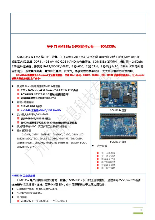
图1 SOM-TL335x正面图2 SOM-TL335x背面由广州创龙自主研发的SOM-TL335x是体积极小的AM335x Cortex-A8工业级核心板。
采用沉金无铅工艺的八层板设计,专业的PCB Layout保证信号完整性的同时,经过严格的质量控制,满足工业各种极端环境应用,不仅提供丰富的Demo程序,还提供详细的开发教程,协助进行底板设计和调试以及软件开发。
2典型运用领域●工业及楼宇自动化●消费类医疗器械●机器人●智能收费系统●充电桩计费控制单元●称重系统●电力仪表3软硬件参数系统框图图3 AM335x功能框图软件参数表 2(2)系统烧写镜像、内核驱动源码、文件系统源码,以及丰富的Demo程序;(3)完整的平台开发包、入门教程,节省软件整理时间,上手容易;(4)基于广州创龙AM335x开发板的Qt界面开发教程;开发例程主要包括:➢TI-RTOS开发例程➢Linux开发例程➢Qt开发例程➢PRU开发例程图5 SOM-TL335x机械尺寸图。