
BAT54TA;BAT54STA;BAT54CTA;BAT54ATA;BAT54TC;中文规格书,Datasheet资料
- 格式:pdf
- 大小:98.21 KB
- 文档页数:3
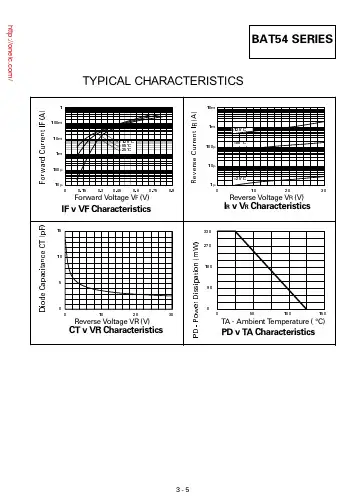
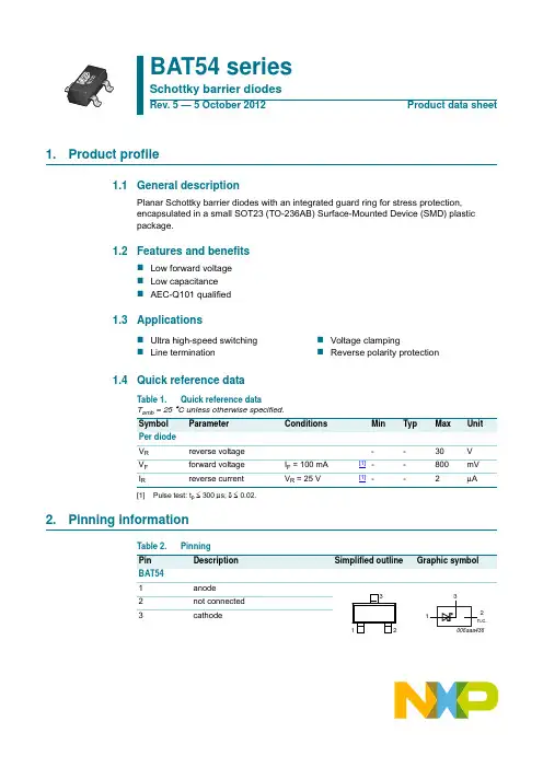

DATA SHEETProduct specificationSupersedes data of 2001Oct 122002Mar 04DISCRETE SEMICONDUCTORSBAT54 seriesSchottky barrier (double) diodes ook, halfpageM3D088Schottky barrier (double) diodes BAT54 seriesFEATURES•Low forward voltage•Guard ring protected•Small plastic SMD package.APPLICATIONS•Ultra high-speed switching•Voltage clamping•Protection circuits•Blocking diodes.DESCRIPTIONPlanar Schottky barrier diodes encapsulated in a SOT23 small plastic SMD package. Single diodes and double diodes with different pinning are available.MARKINGNote1.∗=p:Made in Hong Kong.∗=t:Made in Malaysia.∗=W: Made in China.PINNINGTYPE NUMBER MARKING CODE(1) BA T54L4∗BA T54A L42 or∗V3BA T54C L43 or∗W1BA T54S L44 or∗V4PINDESCRIPTIONBAT54BAT54A BAT54C BAT54S 1a k1a1a12n.c.k2a2k23k a1,a2k1,k2k1,a2 handbook, 2 columns213MGC421Top viewFig.1Simplified outline (SOT23) and pinconfiguration.312MLC360312MLC359312MLC358 Fig.2 Diode configuration and symbol.312n.c.MLC357(1)BAT54(2)BAT54A(3)BAT54C(4)BAT54SSchottky barrier (double) diodesBA T54 series LIMITING VALUESIn accordance with the Absolute Maximum Rating System (IEC 60134).THERMAL CHARACTERISTICSNote1.Refer to SOT23 standard mounting conditions.CHARACTERISTICST amb =25°C unless otherwise specified.SYMBOLPARAMETER CONDITIONS MIN.MAX.UNIT Per diodeV Rcontinuous reverse voltage −30V I Fcontinuous forward current −200mA I FRMrepetitive peak forward current t p ≤1s;δ≤0.5−300mA I FSMnon-repetitive peak forward current t p <10ms −600mA T stgstorage temperature −65+150°C T jjunction temperature −125°C Per deviceP tot total power dissipation T amb ≤25°C −230mW SYMBOLPARAMETER CONDITIONS VALUE UNIT R th j-athermal resistance from junction to ambient note 1500K/W SYMBOLPARAMETER CONDITIONS MAX.UNIT Per diodeV F forward voltage see Fig.3I F =0.1mA240mV I F =1mA320mV I F =10mA400mV I F =30mA500mV I F =100mA800mV I Rreverse current V R =25V; see Fig.42µA t rr reverse recovery time when switched from I F =10mAto I R =10mA; R L =100Ω;measured at I R =1mA;see Fig.65ns C d diode capacitance f =1MHz; V R =1V; see Fig.510pFSchottky barrier (double) diodes BA T54 series handbook, halfpage10I FV F (V)310(mA)21011011.20.80.40MSA892(3)(2)(1)(3)(2)(1)(1)T amb =125°C.(2)T amb =85°C.(3)T amb =25°C.Fig.3Forward current as a function of forward voltage; typical values.0102030V (V)R 103I R (µA)102101101(1)(2)(3)MSA893(1)T amb =125°C.(2)T amb =85°C.(3)T amb =25°C.Fig.4Reverse current as a function of reverse voltage; typical values.handbook, halfpage 0102030051015V R (V)C d(pF)MSA891Fig.5Diode capacitance as a function of reversevoltage; typical values.f =1MHz; T amb =25°C.Fig.6 Reverse recovery definitions.handbook, halfpage 90%10%t f Q dI dttI FI R MRC129 - 1FrSchottky barrier (double) diodesBA T54 series PACKAGE OUTLINE UNITA 1max.b p c D E e 1H E L p Q w v REFERENCES OUTLINEVERSIONEUROPEAN PROJECTION ISSUE DATE 97-02-2899-09-13IEC JEDEC EIAJ mm 0.10.480.380.150.09 3.02.8 1.41.20.95e 1.9 2.52.10.550.450.10.2DIMENSIONS (mm are the original dimensions)0.450.15 SOT23TO-236AB b p D e 1e AA 1L p Qdetail X H E E w M v M AB A B 012 mmscale A 1.10.9cX123Plastic surface mounted package; 3 leads SOT23Schottky barrier (double) diodesBA T54 series DATA SHEET STATUSNotes1.Please consult the most recently issued data sheet before initiating or completing a design.2.The product status of the device(s) described in this data sheet may have changed since this data sheet waspublished. The latest information is available on the Internet at URL .DATA SHEET STATUS (1)PRODUCT STATUS (2)DEFINITIONS Objective data Development This data sheet contains data from the objective specification for productdevelopment. Philips Semiconductors reserves the right to change thespecification in any manner without notice.Preliminary data Qualification This data sheet contains data from the preliminary specification.Supplementary data will be published at a later date. PhilipsSemiconductors reserves the right to change the specification withoutnotice, in order to improve the design and supply the best possibleproduct.Product data ProductionThis data sheet contains data from the product specification. PhilipsSemiconductors reserves the right to make changes at any time in orderto improve the design, manufacturing and supply. Changes will becommunicated according to the Customer Product/Process ChangeNotification (CPCN) procedure SNW-SQ-650A.DEFINITIONSShort-form specification The data in a short-formspecification is extracted from a full data sheet with thesame type number and title. For detailed information seethe relevant data sheet or data handbook.Limiting values definition Limiting values given are inaccordance with the Absolute Maximum Rating System(IEC 60134). Stress above one or more of the limitingvalues may cause permanent damage to the device.These are stress ratings only and operation of the deviceat these or at any other conditions above those given in theCharacteristics sections of the specification is not implied.Exposure to limiting values for extended periods mayaffect device reliability.Application information Applications that aredescribed herein for any of these products are forillustrative purposes only. Philips Semiconductors makeno representation or warranty that such applications will besuitable for the specified use without further testing ormodification.DISCLAIMERS Life support applications These products are not designed for use in life support appliances, devices, or systems where malfunction of these products can reasonably be expected to result in personal injury.Philips Semiconductors customers using or selling these products for use in such applications do so at their own risk and agree to fully indemnify Philips Semiconductors for any damages resulting from such application.Right to make changes Philips Semiconductors reserves the right to make changes,without notice,in the products, including circuits, standard cells, and/or software, described or contained herein in order to improve design and/or performance. Philips Semiconductors assumes no responsibility or liability for the use of any of these products,conveys no licence or title under any patent, copyright, or mask work right to these products,and makes no representations or warranties that these products are free from patent, copyright, or mask work right infringement, unless otherwise specified.。
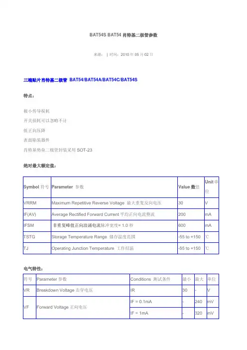
关于肖特基二极管、型号的命名、字母含义、解释肖特基二极管的命名:肖特基二极管是以其发明人肖特基博士(Schottky)命名的,完整的叫法是:肖特基整流二极管(Schottky Rectifier Diode缩写成SR),也有人叫做:肖特基势垒二极管(Schottky Barrier Diode缩写成SBD)的简称。
肖特基:Schottky整流:RectifierSR:即为肖特基整流二极管Schottky Rectifier Diode:肖特基整二极管,简称:SR,比如:SR107,SR10100CT......肖特基:Schottky势垒:BarrierSB:即为肖特基势垒二极管肖特基二极管也称肖特基势垒二极管(简称SBD),国内厂家也有叫做“SB1045CT、SR10100、SL....、BL....Schottky Barrier Diode:肖特基势垒二极管,简称:SB,比如:SB107,SB1045CT......Schottky Barrier Diode:也有简写为:SBD来命名产品型号前缀的。
但SBD不是利用P型半导体与N型半导体接触形成PN结原理制作的,而是利用金属与半导体接触形成的金属-半导体结原理制作的。
因此,SBD也称为金属-半导体(接触)二极管或表面势垒二极管,它是一种热载流子二极管。
关于肖特基MBR系列为什么国际通用常见的肖特基二极管都以“MBR”字头命名?因为最早是世界著名半导体公司-摩托罗拉半导体命名的产品型号M:是以最早MOTOROLA的命名,取MB:Bridge 桥;Barrier:势垒R:Rectifier,整流器 “MBR”意为整流器件SCHOTTKY:肖特基 SCHOTTKY RECTIFIER DIODES:肖特基整流二极管。
例如:MBR10200CTM:MOTOROLA 缩写MB:Barrier缩写BR:Rectifier 缩写R10:电流10A200:电压200VC:表示TO-220AB封装,常指半塑封。