ESD与latchup测试介绍
- 格式:ppt
- 大小:3.58 MB
- 文档页数:51
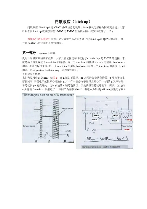
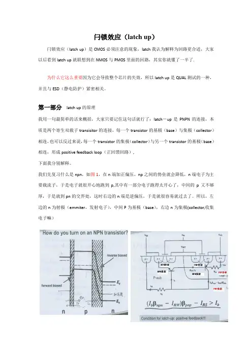
闩锁效应(latch up)闩锁效应(latch up)是CMOS必须注意的现象,latch我认为解释为回路更合适,大家以后看到latch up就联想到在NMOS与PMOS里面的回路,其实你就懂了一半了.为什么它这么重要?因为它会导致整个芯片的失效,所以latch up是QUAL测试的一种,并且与ESD(静电防护)紧密相关。
第一部分 latch up的原理我用一句最简单的话来概括,大家只要记住这句话就行了:latch-up是PNPN的连接,本质是两个寄生双载子transisitor的连接,每一个transistor的基极(base)与集极(collector)相连,也可以反过来说,每一个transistor的集极(collector)与另一个transistor的基极(base)相连,形成positive feedback loop(正回馈回路),下面我分别解释。
我们先复习什么是npn,如图1,在n端加正偏压,np之间的势垒就会降低,n端电子为主要载流子,于是电子就很开心地跑到p,其中有一部分电子跑得太开心了,中间的p又不够厚,于是就到pn的交界处,这时右边的n端是逆偏压,于是就很容易就过去了。
所以,左边的n为射极(emmiter,发射电子),中间P为基极(base),右边n为集极(collector,收集电子嘛)理解了npn,那么pnp就好办,如图2。
图2清楚的表示了latch up的回路。
左边是npn,右边是pnp,图3是电路示意图。
大家可以看出,P-sub既是npn的基极,又是pnp的集极;n-well既是既是pnp的基极,又是npn的集极,所以说,每一个transistor的集极(collector)与另一个transistor的基极(base)相连。
那么电流怎么走呢?比如在P+加5V-->电洞被从P+推到N well-->越过n well再到p sub-->这个时候,大家注意,电洞有两条路可走,一是跑到NMOS的N+,二是跑到旁边的Nwell,nwell比n+深,当然更好去,所以电洞又回去了。
ESD测试方法范文ESD(Electrostatic Discharge,静电放电)是指当带电物体与不带电物体接触或彼此之间接触时,由于静电荷的变化而产生的瞬间放电现象。
ESD可能对电子设备、电子元器件等造成损坏,因此对于电子产品的设计和制造过程中,需要进行ESD测试以保证产品的质量和可靠性。
ESD测试是为了评估电子设备或电子元器件在实际使用中遭遇ESD时的抗干扰能力。
在日常生活中,我们可能经常会遇到ESD,比如在干燥的天气中穿着羊毛衣服摩擦后触摸电子设备,或者在走地毯的地方穿着尼龙袜触碰电子产品等。
这些情况下,如果电子产品没有经过足够的ESD测试,就有可能会受到损坏。
1.人工模拟ESD事件:这种方法是通过模拟人类身体ESD时的放电过程,使用带有特殊电阻的手套或者鞋底,在实验室中进行ESD测试。
测试人员会穿着特殊的防护服,通过接地线将自己接地,然后使用手套或鞋底进行放电操作,模拟ESD事件对电子产品的影响。
2.放电枪测试:这种方法是使用专门设计的放电枪对电子设备进行ESD测试。
放电枪会产生高电压的电荷,并在固定的距离处对电子设备进行放电,模拟真实的ESD事件。
通过观察电子设备的响应和表现来评估其抗ESD能力。
3.金属小球测试:这种方法是通过将金属小球带电并接触电子设备表面,从而产生ESD事件。
可以通过控制金属小球的带电量和放电时间来模拟不同强度的ESD事件,评估电子设备的抗ESD能力。
除了以上几种常见的ESD测试方法,还有一些其他的测试方法,比如ESD击穿测试、ESD抑制测试等。
这些测试方法可以根据实际需要选择和组合,以确定电子产品的ESD性能。
对于ESD测试,有一些常见的参数和标准需要关注,比如放电强度、放电时间、放电波形等。
这些参数和标准可以帮助我们评估电子产品在不同ESD事件下的响应情况,从而优化产品设计和制造过程,提高产品的质量和可靠性。
总的来说,ESD测试是一个非常重要的环节,对于保证电子产品的质量和可靠性至关重要。

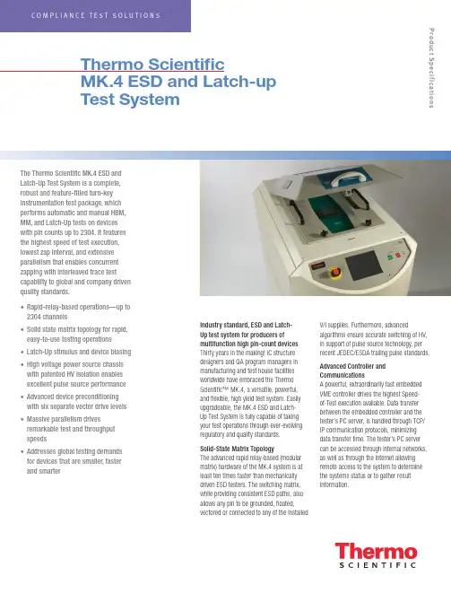
The Thermo Scientific MK.4 ESD and Latch-Up Test System is a complete,robust and feature-filled turn-key instrumentation test package, which performs automatic and manual HBM, MM, and Latch-Up tests on devices with pin counts up to 2304. It features the highest speed of test execution, lowest zap interval, and extensive parallelism that enables concurrent zapping with interleaved trace test capability to global and company driven quality standards.• Rapid-relay-based operations—up to 2304 channels• Solid state matrix topology for rapid, easy-to-use testing operations • Latch-Up stimulus and device biasing • High voltage power source chassis with patented HV isolation enables excellent pulse source performance • Advanced device preconditioning with six separate vector drive levels • Massive parallelism drives remarkable test and throughput speeds• Addresses global testing demands for devices that are smaller, faster and smarterThermo ScientificMK.4 ESD and Latch-up Test SystemIndustry standard, ESD and Latch-Up test system for producers ofmultifunction high pin-count devices Thirty years in the making! IC structure designers and QA program managers in manufacturing and test house facilities worldwide have embraced the Thermo Scientific™ MK.4, a versatile, powerful, and flexible, high yield test system. Easily upgradeable, the MK.4 ESD and Latch-Up Test System is fully capable of taking your test operations through ever-evolving regulatory and quality standards.Solid-State Matrix TopologyThe advanced rapid relay-based (modular matrix) hardware of the MK.4 system is at least ten times faster than mechanically driven ESD testers. The switching matrix, while providing consistent ESD paths, also allows any pin to be grounded, floated,vectored or connected to any of the installedV/I supplies. Furthermore, advancedalgorithms ensure accurate switching of HV, in support of pulse source technology, per recent JEDEC/ESDA trailing pulse standards.Advanced Controller and CommunicationsA powerful, extraordinarily fast embedded VME controller drives the highest Speed- of-Test execution available. Data transfer between the embedded controller and the tester’s PC server, is handled through TCP/IP communication protocols, minimizing data transfer time. The tester’s PC server can be accessed through internal networks, as well as through the internet allowing remote access to the system to determine the systems status or to gather result information.Product SpecificationsLatch-Up Stimulus and Device Biasing The MK.4 can be equipped with up to eight 100 V four-quadrant Voltage and Current (V/I) power supplies. Each V/I supply has a wide dynamic range enabling it to force and measure very low voltage at high current levels from 100 mV/10 A to 100 V/1 A. The system’s power supply matrix can deliver up to a total of 18A of current, which is distributed between the installed supplies. These supplies are able to provide a fast and versatile means of making DC parametric and leakage measurements as well as providing latch-up pulses, while offering total control and protection of the DUT.Advanced Device PreconditioningThe MK.4 system provides the most advanced device preconditioning capability available. The DUT can be vectored with complex vector patterns, providing excellent control over the device. Each pin can be driven using one of the 6 different vector supplies. The patterns can be up to 256k deep, running at clock speeds of up to 10 MHz. Device conditioning is easily verified, using the read back compare capability available on every pin.Thermo Scientific MK.4 Scimitar™Software Makes Programming Easy, while Providing Unsurpassed Programming FlexibilityThe MK.4 Windows®-based Scimitar operating software empowers users with the flexibility to easily set-up tests based on industry standards or company driven requirements.Device test plans can be created by importing existing text based device files, on the testers PC server or off-line from a satellite PC containing the application. The software also provides the capabilities to import test plans and device files from previous Thermo Scientific test systems.Test vectors from your functional testers can also be imported into the application. And of course, the vector application allows manual creation and debug of vector files.Device test plans and results are stored in an XML data base, providing unsurpassed results handling, sorting and data mining capabilities.Parallelism Drives Remarkable Test Throughput SpeedsThe MK.4 software enables ESD testing of up to twelve devices at one time using the multisite pulse source design.Embedded VME power supplies eliminate any communication delays that would be seen by using stand alone supplies. The embedded parametric (curve tracing) supply also provides fast, accurate curve tracing data to help you analyze your devices performance.The systems curve tracer can also be used as a failure analysis tool by allowing the comparison of stored, known good results, versus results from a new test sample or samples.Ready for Today’s Component Reliability Demands and Anticipating Those to Come ESD and Latch-Up testing of electronic and electrical goods can be very expensive aspects of the design and manufacturing process. This is especially true as market demands for products that are smaller, faster and smarter become the standard rather than the exception. The Thermo Scientific MK.4 leverages the technology and know- how gained over three decades of test system experience, as well as our in-depth participation and contributions to global regulatory bodies governing these changes, enabling today’s products to meet both global and industry-driven quality standards.The real key to our customers’ success is in anticipating what’s next. And to ensure that our customers possess the ability to evolve quickly to meet all change factors with efficiency and cost effectiveness.As such, the strategically-designed, field upgradeable architecture of the MK.4 system ensures a substantial return on investment over a very considerable test system lifecycle, as well as better short- and long-term qualityand ESD and Latch-Up test economies.Custom fixtures include universal package adaptors to enable the industry’s lowest cost-in-service high pin count device fixturing yetdevised. (2304-pin, Universal 1-mm pitch BGA package adaptor shown.)100W V/I Performance Thermo Scientific MK.4: eight-V/I configuration. Powerful V/Is can deliver a total of 800 W to the DUT, enabling complex testing of all advanced high power processors on your product roadmap.Solid state matrix topology for rapid, easy-to-use testing operations. Design ensures waveform integrity and reproducibility.General SpecificationsHuman Body Model (HBM) per ESDA/JEDEC JS-001-2014, MIL-STD 883E, and AEC Q100-002 25 V to 8 kV in steps of 1 V Test to multiple industry standards in one integrated system; no changing or alignment of pulse sources.Wizard-like prompts on multi-step user actions MachineModel (MM) per ESDA STM5.2, JEDEC/JESD22-A115, andAEC Q100-003, 25 V to 1.5 kV in steps of 1 VIntegrated pulse sources allow fast multi-site test execution.Latch-up testing per JEDEC/JESD 78 test pin and AECQ100-004Includes preconditioning, state read-back and full control of each.Rapid Relay-based operations at least 10 times faster thanrobotic-driven testersSuper fast test speeds.Test devices up to 2304 pins Systems available configured as 1152, 1728 or 2304 pins.Waveform network: Two, 12 site HBM (100 pF/1500Ω)and MM (200 pF/0Ω) pulse sources address up to 12devices simultaneouslyPatented design ensures waveform compliance for generations to come.Multiple device selection When multiple devices are present; graphical display indicates the devices selectedfor test; progress indicator displays the current device under test (DUT), along withtest status information.Unsurpassed software architecture Flexible programming, easy to use automated test setups, TCP/IP communication. Enables use of device set-up information Increased efficiency and accuracy from other test equipment, as well as deviceinformation import.Event trigger output Manages setup analysis with customized scope trigger capabilities.High voltage power supply chassis Modular chassis with patented HV isolation enables excellent pulse sourceperformance.Power supply sequencing Provides additional flexibility to meet more demanding test needs of integratedsystem-on-chip (SOC) flexibility.Manages ancillary test equipment through Plug-n feature allows the user to control external devices, such as scopes or heatstreams or other devices the Scimitar Plug-ins feature as required for automatedtesting.Pin drivers for use during Latch-Up testing Vector input/export capability from standard tester platforms and parametricmeasurements.256k vectors per pin with read-back Full real-time bandwidth behind each of the matrix pins.Six independent vector voltage levels Test complex I/O and Multi-Core products with ease.Up to 10MHz vector rate (programmable) Quickly and accurately set the device into the desired state for testing from an internalclock.Comprehensive engineering vector debug. Debug difficult part vectoring setups with flexibility.Up to eight separate V/I supplies (1 stimulus and 7 bias supplies) capability through the V/I matrix High accuracy DUT power, curve tracing, and Latch-up stimulus available; design also provides high current.Low resolution/high accuracy parametric measurements, using an embedded Keithley PSU With the optional Keithley PSU feature (replaces one V/I, nA measurements are achievable, allowing supply bus resistance measurement analysis to be performed.Multiple self-test diagnostic routines Ensures system integrity throughout the entire relay matrix, right up to the test socket Test reports: pre-stress, pre-fail (ESD) and post-fail data,as well as full curve trace and specific data pointmeasurementsData can be exported for statistical evaluation & presentation.Individual pin parametrics Allows the user to define V/I levels, compliance ranges, and curve trace parametersfor each pin individually.Enhanced data set features Report all data gathered for off-line reduction and analysis; core test data is readilyavailable; all data is stored in an easy-to-manipulate standard XML file structure. Interlocked safety cover Ensures no user access during test. All potentially lethal voltages are automaticallyterminated when cover is opened. Safety cover window can be easily modified toaccept 3rd party thermal heads.Dimensions60 cm (23.5 in) W x 99 cm (39 in) D x 127 cm (50 in) H© 2016 Thermo Fisher Scientific Inc. All rights reserved. Windows is a registered trademark of Microsoft Corporation in the United States and/or other countries. All other trademarks are the property of Thermo Fisher Scientific and its subsidiaries. Results may vary under different operating conditions. Specifications, terms and pricing are subject to change. Not all products are available in all countries. Please consult your local sales representative for details.Africa-Other +27 11 570 1840 Australia +61 2 8844 9500 Austria +43 1 333 50 34 0 Belgium +32 53 73 42 41 Canada +1 800 530 8447 China +86 10 8419 3588 Denmark +45 70 23 62 60 Europe-Other +43 1 333 50 34 0Finland /Norway/Sweden+46 8 556 468 00France +33 1 60 92 48 00Germany +49 6103 408 1014India +91 22 6742 9434Italy +39 02 950 591Japan +81 45 453 9100Latin America +1 608 276 5659Middle East +43 1 333 50 34 0Netherlands +31 76 579 55 55South Africa +27 11 570 1840Spain +34 914 845 965Switzerland +41 61 716 77 00UK +44 1442 233555USA +1 800 532 4752Thermo Fisher Scientific,San Jose, CA USA is ISO Certified. CTS.05102016Product SpecificationsScimitar Software FeaturesSummary Panel with easy navigation among device componentsWizard-like prompts on multi-step user actionsControl of external devices through the use of Scimitar’s user programmable Plug-in capabilities, in addition to the Event Trigger Outputs, which provide TTL control signals for external devices, such as power supplies or for triggering oscilloscopesFlexible parametric tests that are defined and placed at an arbitrary position within the executable test plan.Comprehensive results viewer that provides:• ESD and Static Latch-up data viewing capabilities• Curves viewer with zooming capabilities and the ability to add user comments• Data filtering on the following criteria – failed pins, failed results, final stress levels• A complete set or subset of results using user defined parameters• Sorting in ascending or descending order by various column criteriaTree-like logical view of the tests and test plans.Flexible data storage that provides the ability for the end-user to query the dataSeamless support of existing ZapMaster, MK.2, MK.4, and Paragon test plansCurve tracing with curve-to-curve and relative spot-to-spot comparisonOff-line curve analyzing, including third-party generated waveformsCanned JESD78A test (static latch-up only) that can be defined automaticallyPause/Resume test capabilitiesIntermediate results viewingAutomated waveform capture capability and analysis using the embedded EvaluWave software feature。
esd测试方法ESD测试方法。
静电放电(ESD)是指在两个不同电势之间发生的突然放电现象。
在现代电子产品中,ESD对设备的损害是一个严重的问题。
因此,为了确保电子设备的可靠性和稳定性,需要对电子设备进行ESD测试。
本文将介绍ESD测试的方法和步骤。
1. ESD测试设备准备。
首先,进行ESD测试需要准备相应的测试设备。
通常,ESD测试设备包括ESD发生器、测试台和测试夹具。
ESD发生器用于产生静电放电,测试台用于放置被测试设备,测试夹具用于连接ESD发生器和被测试设备。
在进行ESD测试之前,需要确保测试设备的正常运行和准确性。
2. ESD测试环境准备。
在进行ESD测试之前,需要准备一个符合标准的测试环境。
测试环境应该是一个无静电干扰的环境,通常采用静电防护地板和静电防护工作服来防止静电的积累。
此外,还需要使用静电计来监测测试环境中的静电水平,确保测试环境符合标准要求。
3. ESD测试标准选择。
在进行ESD测试之前,需要选择适当的ESD测试标准。
常用的ESD测试标准包括IEC 61000-4-2、ANSI/ESD S20.20等。
不同的电子设备可能需要符合不同的ESD测试标准,因此需要根据具体的产品要求选择相应的标准。
4. ESD测试步骤。
进行ESD测试时,通常需要按照以下步骤进行:a. 设置ESD测试参数,根据所选的ESD测试标准,设置相应的测试参数,包括放电电压、放电波形等。
b. 连接测试夹具,将被测试设备连接到测试夹具上,确保连接稳固可靠。
c. 进行ESD测试,根据测试标准要求,对被测试设备进行ESD测试,记录测试结果。
d. 分析测试结果,根据测试结果,评估被测试设备的ESD抗性能力,确定是否符合标准要求。
5. ESD测试结果评估。
在进行ESD测试后,需要对测试结果进行评估。
通常,ESD测试结果包括通过、不通过和边界三种情况。
通过的测试结果表示被测试设备在ESD测试中表现良好,能够抵御静电放电的影响;不通过的测试结果表示被测试设备在ESD测试中出现故障或损坏;边界的测试结果表示被测试设备在ESD测试中表现一般,需要进一步评估和分析。
闩锁效应(latch up)闩锁效应(latch up)是CMOS必须注意的现象,latch我认为解释为回路更合适,大家以后看到latch up就联想到在NMOS与PMOS里面的回路,其实你就懂了一半了.为什么它这么重要因为它会导致整个芯片的失效,所以latch up是QUAL测试的一种,并且与ESD(静电防护)紧密相关。
第一部分latch up的原理我用一句最简单的话来概括,大家只要记住这句话就行了:latch-up是PNPN的连接,本质是两个寄生双载子transisitor的连接,每一个transistor的基极(base)与集极(collector)相连,也可以反过来说,每一个transistor的集极(collector)与另一个transistor的基极(base)相连,形成positive feedback loop(正回馈回路),下面我分别解释。
我们先复习什么是npn,如图1,在n端加正偏压,np之间的势垒就会降低,n端电子为主要载流子,于是电子就很开心地跑到p,其中有一部分电子跑得太开心了,中间的p又不够厚,于是就到pn的交界处,这时右边的n端是逆偏压,于是就很容易就过去了。
所以,左边的n为射极(emmiter,发射电子),中间P为基极(base),右边n为集极(collector,收集电子嘛)理解了npn,那么pnp就好办,如图2。
图2清楚的表示了latch up的回路。
左边是npn,右边是pnp图3是电路示意图。
大家可以看出,P-sub既是npn的基极,又是pnp的集极;n-well既是既是pnp的基极,又是npn的集极,所以说,每一个transistor的集极(collector)与另一个transistor的基极(base)相连。
那么电流怎么走呢比如在P+加5V-->电洞被从P+推到N well-->越过n well再到p sub-->这个时候,大家注意,电洞有两条路可走,一是跑到NMOS的N+,二是跑到旁边的Nwell,nwell比n+深,当然更好去,所以电洞又回去了。
ESD的原理和测试微波与电磁兼容轻松学习微波与电磁兼容的基础知识.静电放电(ESD: Electrostatic Discharge),应该是造成所有电⼦元器件或集成电路系统造成过度电应⼒(EOS: Electrical Over Stress)破坏的主要元凶。
因为静电通常瞬间电压⾮常⾼(>⼏千伏),所以这种损伤是毁灭性和永久性的,会造成电路直接烧毁。
所以预防静电损伤是所有IC设计和制造的头号难题。
静电,通常都是⼈为产⽣的,如⽣产、组装、测试、存放、搬运等过程中都有可能使得静电累积在⼈体、仪器或设备中,甚⾄元器件本⾝也会累积静电,当⼈们在不知情的情况下使这些带电的物体接触就会形成放电路径,瞬间使得电⼦元件或系统遭到静电放电的损坏(这就是为什么以前修电脑都必须要配戴静电环托在⼯作桌上,防⽌⼈体的静电损伤芯⽚),如同云层中储存的电荷瞬间击穿云层产⽣剧烈的闪电,会把⼤地劈开⼀样,⽽且通常都是在⾬天来临之际,因为空⽓湿度⼤易形成导电通到。
那么,如何防⽌静电放电损伤呢?⾸先当然改变坏境从源头减少静电(⽐如减少摩擦、少穿⽺⽑类⽑⾐、控制空⽓温湿度等),当然这不是我们今天讨论的重点。
我们今天要讨论的是如何在电路⾥⾯设计保护电路,当外界有静电的时候我们的电⼦元器件或系统能够⾃我保护避免被静电损坏(其实就是安装⼀个避雷针)。
这也是很多IC设计和制造业者的头号难题,很多公司有专门设计ESD的团队,今天我就和⼤家从最基本的理论讲起逐步讲解ESD保护的原理及注意点,你会发现前⾯讲的PN结/⼆极管、三极管、MOS管、全都⽤上了……以前的专题讲解PN结⼆极管理论的时候,就讲过⼆极管有⼀个特性:正向导通反向截⽌(不记得就去翻前⾯的课程),⽽且反偏电压继续增加会发⽣雪崩击穿(Avalanche Breakdown)⽽导通,我们称之为钳位⼆极管(Clamp)。
这正是我们设计静电保护所需要的理论基础,我们就是利⽤这个反向截⽌特性让这个旁路在正常⼯作时处于断开状态,⽽外界有静电的时候这个旁路⼆极管发⽣雪崩击穿⽽形成旁路通路保护了内部电路或者栅极(是不是类似家⾥⽔槽有个溢⽔⼝,防⽌⽔龙头忘关了导致整个卫⽣间⽔灾)。
ESD测试方法大全资料ESD(静电放电)测试是一种用于测试和评估电子设备、元件及其他电气产品是否能够有效抵御静电放电引起的损坏或干扰的方法。
ESD测试方法包括以下几种:1. 静电放电仿真测试(ESD Simulator Test)这种测试是一种模拟真实环境中可能遇到的静电放电情况的方法,通过使用专门的ESD仿真仪器将已经充电的电容器的电荷释放到被测试设备上,观察设备的反应以及是否会发生故障。
2. 电离空气辐射模拟测试(Charged Device Model,CDM)这种测试方法是一种模拟电子元器件在机械操作和人为接触时受到的静电放电情况的方法。
其原理是通过使用一种特殊的电离空气辐射源,将静电能量转移到被测试设备上,检测设备是否受到损坏或干扰。
3. 电场测试(Electric Field Test)这种测试方法是一种模拟在使用过程中可能遇到的不同电场强度的情况,用以评估设备对不同电场强度的抵抗能力。
测试时,使用专门的电场测试仪器,将设备暴露在不同电场中,并观察设备的反应以及是否会发生故障。
4. 静电放电枪测试(ESD Gun Test)这种测试方法是一种模拟日常生活中可能遇到的静电放电情况的方法,通过使用专门的静电放电枪,向被测试设备释放特定的静电电荷,并观察设备的反应以及是否会发生故障。
5. 四象限测试(Four-quadrant Test)这种测试方法是一种综合了静电放电仿真测试和电场测试的方法。
测试时,使用专门的测试设备将设备暴露在不同电场和电荷释放的情况下,并观察设备的反应,以评估设备对不同静电放电情况的敏感性。
6. 瞬态浪涌测试(Transient Surge Test)这种测试方法是一种用于测试设备在遭受瞬态浪涌电流干扰时的抵抗能力的方法。
测试时,使用专门的浪涌测试仪器将浪涌电流施加到被测试设备上,并观察设备的反应以及是否会发生故障。
7. 耐压测试(Voltage Endurance Test)这种测试方法是一种用于测试设备在高电压下的工作情况的方法。
ESD & Latch-UpPROPRIETARY AND CONFIDENTIAL© Copyright 2009 Evans Analytical Group LLC1Electrostatic Discharge 静电放电ESD (Electrostatic Discharge) 的现象通常表现就像在干燥的 空气里指尖碰触到门把手,感 觉到一次突然的电击。
造成这种电击的原因是人体和 零电位的 门把表面间产生的离 子化效应。
ESD可以解释为是一种电荷从 一个物体释放到另一个物体的 过程。
PROPRIETARY AND CONFIDENTIAL© Copyright 2009 Evans Analytical Group LLC2ESD失效比例 在半导体工业中,因半导体器件的集成度越来越高,工 艺越来越复杂,IC中潜在的破坏性的ESD 变得越来越 重要和典型。
在小器件中,电场高压和高密度的电流将 会导致电路里面的电阻损坏或者热破坏 (breakdown of insulators and thermal damage)。
这些因为ESD而 。
造成IC失效如果没有得到有力地研究原因和解决方法, 这对芯片的退出使用将是致命的。
在硅器件失效模型 分布中,在接近 50%的EOS案例中 大约有10%是ESD 引起的失效。
引自ESD in Silicon Integrated Circuit (Second Edition)3PROPRIETARY AND CONFIDENTIAL© Copyright 2009 Evans Analytical Group LLC静电放电测试模型HBM-Human Body Model(人体模式)人体放电模式是指因人体在地上走动摩擦或其他因素在人体上已累积了静电,当此 人触接近于一个接地的IC器件,当指尖和IC的其中一个pin脚在空气中产生作用 (break down) 的时候,人体上的静电便会经由IC的管脚进入到IC内,再经由IC放电到地。
esd测试方法ESD测试方法。
1. 背景介绍。
ESD(Electrostatic Discharge)是静电放电的英文缩写,是指当两个物体之间的电位差达到一定数值时,会发生突然放电现象。
ESD对电子设备和元器件可能造成损坏,因此需要对其进行测试,以保证产品的可靠性和稳定性。
2. ESD测试的重要性。
ESD测试是电子产品开发和生产过程中非常重要的一环。
通过对产品进行ESD测试,可以评估其在静电放电环境下的抗干扰能力,从而保证产品在实际使用中不会因为静电放电而损坏,提高产品的可靠性和稳定性。
3. ESD测试方法。
3.1 ESD测试设备。
ESD测试设备通常包括ESD发生器、ESD探针、测试台等。
ESD 发生器用于产生静电放电,而ESD探针用于模拟人体或其他物体的放电过程,测试台用于放置被测试产品。
3.2 ESD测试流程。
(1)准备工作,将被测试产品放置在测试台上,并连接ESD发生器和ESD探针。
(2)设定参数,根据产品的规格要求,设定ESD发生器的放电能量和频率。
(3)测试过程,通过操作ESD发生器,对被测试产品进行静电放电,观察产品的反应情况。
(4)数据记录,记录产品在不同放电能量下的反应情况,包括是否出现故障、是否影响产品功能等。
(5)分析评估,根据测试数据,评估产品的抗ESD能力,确定是否符合规格要求。
3.3 ESD测试标准。
ESD测试通常遵循国际上通用的标准,如IEC 61000-4-2。
该标准规定了不同级别的ESD放电能量和频率,以及测试过程和评估方法,对于产品的ESD抗干扰能力提出了具体要求。
4. 结语。
ESD测试是保证电子产品质量的重要环节,通过合理的测试方法和标准,可以有效评估产品的抗ESD能力,提高产品的可靠性和稳定性,减少因静电放电而造成的损坏。
希望本文介绍的ESD测试方法能为相关领域的工程师和研究人员提供参考,提升产品的质量和竞争力。