光学二次谐波产生及光混频前三节PPT
- 格式:ppt
- 大小:835.50 KB
- 文档页数:14

Engineering the second harmonic generation pattern from coupled gold nanowiresA.Benedetti,M.Centini,*C.Sibilia,and M.BertolottiDipartimento di Energetica,Universitàdi Roma,La Sapienza,Via A.Scarpa16,00161Roma,Italy*Corresponding author:marco.centini@uniroma1.itReceived November2,2009;accepted December16,2009;posted January5,2010(Doc.ID119439);published February4,2010We numerically investigated second harmonic generation from systems composed of two coupled gold nano-wires.The developed method allows one to arbitrarily change the shape of the wire cross section in order to explore the generated and scatteredfield patterns.Our results suggest that the overall second harmonic gen-eration is related to the electromagnetic energy per unit length stored in the gap area between the wires.These geometrical considerations make further optimization possible.As an example we discuss the possibility to select dipolar emission and/or quadrupolar emission patterns.The selection mechanism responsible for this kind of emission can be traced back to the interaction between nonlinear sources with the surface plasmon resonance of the metallic wires.©2010Optical Society of AmericaOCIS codes:160.4330,190.3970,190.4350,290.5850.1.INTRODUCTIONThe second order nonlinear response fromflat metal screens has been widely investigated,both theoretically and experimentally,from the late1960s–1980s[1–11]. Some of this work was devoted to the study of the second harmonic generation(SHG)in reflection by thin metal layers and/or metallic gratings,with the subsequent re-porting of the enhancement of nonlinear conversion effi-ciencies due to the surface plasmon polariton(SPP)exci-tation at the metal/dielectric interface[12–15].Regarding the SHG in systems composed of many metallic particles and/or percolated systems,several models have been pro-posed that utilize the effective medium approximation and experimental techniques have been developed to characterize the nonlinear optical responses[16–20]. Also,a large number of works have been devoted to the study of materials and single molecule behavior to en-hance and characterize the nonlinear response[21–27].The last few years witnessed renewed interest in the study of nonlinear second order properties of metal/ dielectric composites thanks to the development of nano-technologies and nanoscience.The SHG has been de-tected in metal nanoparticles and the effects of scatterer size on the dipole or multipole contributions have been ex-perimentally investigated[28,29].A strong second har-monic(SH)signal has been found emanating from sharp metal tips[30],thus opening the way to interesting appli-cations for nearfield nonlinear microscopy and spectros-copy.The SHG enhancement from nanoantennas and nanodimers has been observed both in near and farfields [31–34].Other recent works[35,36]deal with the SHG in gold nanowires.In these studies the effect offield polar-ization direction with respect to the direction of the wires is emphasized.Moreover,the SHG from metamaterials composed of split-ring resonators was experimentally re-ported by Klein et al.[37,38].Another experimental pa-per,recently published,reports the SHG from a gold plate having a periodic pattern of rectangular apertures on top [39].In[39]the effect reported is connected to the shape of the apertures and to the propagation constants of the guided electromagnetic(e.m.)modes inside the apertures. This feature has been employed to enhance the nonlinear response of GaAs using it tofill patterned metallic screens with holes,taking advantage of the high trans-mission regime and strongfield localization inside the holes[40].All these aspects,combined with the state of art technology capabilities,make these materials very in-teresting for basic and applied research.From a theoretical point of view,the farfield pattern of the generated SH has been studied in detail for a single metallic cylinder or other two-dimensional(2D)single ob-jects as well as for nanospheres and deformed nano-spheres[41–45].Also,the scattered SH generated by a SPP at a surface nanodefect was theoretically investi-gated[46].Recent works report on numerical results ob-tained by the implementation of afinite difference time domain(FDTD)algorithm[47–50].Reference[48]deals with the SHG from resonant nanoslits on a silver sub-strate,by taking into account the nonlinearity arising in the free electron response from the magnetic Lorentz force.In[47]the quantum jellium model[10]for the non-linear response of a metal was implemented in a FDTD algorithm;numerical results are shown for periodically patterned metallic screens.Limitations of the validity of the approach used in[47]for nanostructured objects are related to the parameterization procedure used for the nonlinear coefficient of the metal,performed assuming an infiniteflat surface.In[49]a semiclassical approach, based on the free electron gas model for the nonlinear op-tical response of a metal,has been adopted to successfully analyze experimental results of[50].Also,in[51]the au-thors showed that for patterned metallic membranes hav-0740-3224/10/030408-9/$15.00©2010Optical Society of Americaing thicknesses of a few tens of nanometers the farfield SH is dominated by dipole contributions of the nonlinear response.In this work we study the enhancement of the SHG due to the interaction between two2D metallic wires with sec-tions of arbitrary shape,focusing on the possibility of tai-loring the emission pattern by properly designing the shape and the position of the wires.Numerical calcula-tions on two different kinds of double-wire systems,rect-angular section(RS)and trapezoidal section(TS)of the wires,are performed.The SHG as a function of the dis-tance(air gap)between the wires is investigated in both the near and farfield regimes.The enhancement of the SH signal is then explained in terms of the pump energy stored inside the gap.Our results reveal a high sensitivity of the emission pattern and the overall power with re-spect to displacements of just a few nanometers.In par-ticular we show that the SHfield with dipole and quad-rupole symmetries can be achieved by changing the geometrical parameters.Although we only consider sys-tems composed of two wires,our approach can be applied for an arbitrary number of objects with different shapes and sizes.Wefinally investigate localization effects of the SHfield at the surface,revealing the existence of hot spots that can be used for nanoillumination and single molecule spectroscopy[52].The paper is divided into four main sections:Following this introduction,in Section2,we describe the used the-oretical model and integration method.In Section3we show the results of our numerical analysis focusing our attention on the different behaviors of emittedfields as functions of the nano-object shape and position.Finally, in Section4the main conclusions and perspectives for fu-ture work are drawn.2.THEORETICAL MODELAt optical frequencies the linear response of a metal is strongly affected by the bound valence electrons.We chose to model the electric permittivity of gold from the far infrared to the ultraviolet range with a Drude–Lorentz model by consideringfive Lorentz-like[53–55] resonators,r͑͒=D͑͒+͚k=15G kP20,k2−2−i␥k,D͑͒=1−G0P2͑+i␥0͒=1−02͑+i␥0͒,͑1͒whereD is the electric permittivity obtained by consider-ing the Drude model only.p is the plasma frequency as-sociated with the total number of electrons per unit vol-ume.G k and0,k are,respectively,the oscillator strengths and resonant frequencies and␥k are damping constants related to each oscillator.0=ͱG0p is the plasma fre-quency associated with intraband transitions(relatedonly to the free electron density)with damping constant ␥0.Indeed we assume that,in the absence of external ex-citation,the free electron density n is constant and equal to its bulk value n0,being02=͑e2n0/m0͒,where e is the absolute value of the electron charge and m is the effec-tive electron mass.The values of the parameters of the Drude–Lorentz model are reported in[53].We model the optical response of the metal by assum-ing an effective current density,Jជ=JជD+ץPជb.e.ץt,͑2͒where JជD is the current density induced by the e.m.field on the free electrons and Pជb.e.is the polarization vector due to the presence of bound electrons.Each term on the right hand side of Eq.(2)contains both linear and nonlin-ear contributions.At this stage we focus our attention on the nonlinear contributions arising from conduction elec-trons only.We study the SHG process in the undepleted pump ap-proximation from a metallic2D structure that reacts in the presence of a transverse magnetic͑p-͒polarized e.m.field;the system is completely2D.The nonlinear second order response of the conduction electrons is then evalu-ated as in[49]and the dynamic equations for JជD and n areץJជDץt=JជDneٌជ·JជD+͑JជD·ٌជ͒JជDne−␥0JជD+e2mnEជ−e0mJជD∧Hជ,͑3aٌ͒ជ·JជD=eץnץt,͑3b͒where␥0is defined in Eqs.(1)and it represents losses due to Coulomb scattering of conduction electrons with the lattice ions.By adopting a perturbative approach as in[8]we move into the frequency domain and write the current density at the SH frequency as a function of the fundamental fre-quency(FF)field by collecting terms up to the second or-der.Thus,the expressions of thefields,the current,and free electron densities areJជ͑rជ,t͒=͚m=1,2Jជm͑rជ͒e−imt+c.c.,Eជ͑rជ,t͒=͚m=1,2Eជn͑rជ͒e−imt+c.c.,Hជ͑rជ,t͒=͚m=1,2Hជm͑rជ͒e−imt+c.c.,n͑rជ,t͒=n0+͚m=1,2n m͑rជ͒e−imt+c.c.,͑4͒where the subscript m=1,2refers to the FF͑͒and SH ͑2͒angular frequencies.Due to the weak nature of the nonlinear interaction,we consider that the dynamics for the FF is completely described by the linear response,Jជ1=−i͑r,1−1͒0Eជ1,͑5͒wherer,1is calculated by using Eqs.(1).For the SHfield we haveJ 2ជ=−i 20r ,2E 2ជ−i 20ͫabE 1ជٌជ·͓D ,1E 1ជ͔+b ͑a −1͒D ,12͑E 1ជ·ٌជ͒E 1ជ+bD ,14ٌជ͓E 1ជ·E 1ជ͔ͬ,͑6͒wherea =+i ␥0,b =22+i ␥0,=−e 2m 2,͑7͒and r ͑r ជ͒=r ͑r ជ͒−1,D ͑r ជ͒=D ͑r ជ͒−1are the expressionsfor the spatially dependent electric susceptibility accord-ing to the definitions given in Eqs.(1).We note that the coefficients a and b are exactly equal to unity in the case of no losses.The first term on the right hand side of Eq.(6)represents the linear contribution,which depends on both bound and free electrons;the remaining terms are the nonlinear sources.The evaluation of the nonlinear terms of Eq.(6)requires a detailed analysis to separate bulk and surface contributions.In the bulk,the first non-linear term of Eq.(6)vanishes and the other terms,evalu-ated only for the points inside the metallic objects,are re-sponsible for the bulk contribution to the nonlinear current density,J ជNL Bulk =−i 20D ,12b ͫ͑a −1͒͑E 1ជ·ٌជ͒E 1ជ+12ٌជ͓E 1ជ·E 1ជ͔ͬ.͑8͒In order to evaluate surface contributions we assume thatthe transition from metal to surrounding air is achieved by varying the value of the parameter P 2from the value it assumes in the metal to zero in the vacuum.Thus the other parameters,i.e.,damping coefficients and electron effective mass,are considered as constant coefficients.Following the procedure outlined in [56],modified and adapted to our case (losses and linear contribution of bound electrons),we evaluate the nonlinear surface cur-rents acting as sources for the SH field,X ˆ·J ជNL Surface =−i 20abE 1,X ͑−͒E 1,Y ͑−͒͑1−D ,1͒␦͑Y ͒,Y ˆ·J ជNL Surface =−i 20ab ͓E 1,Y͑−͔͒24͓͑1−D ,1͒͑r ,1+3͔͒␦͑Y ͒.͑9͒Calling r ជЈthe vectors defining the coordinates of theboundaries,X ˆ͑r Јជ͒and Yˆ͑r Јជ͒are the local unit vectors tan-gential and normal (outgoing)to the surface,respectively.In order to provide a comparison with previous results wechoose to evaluate the continuous function r ,1͑r Јជ͒E 1,Y ͑r Јជ͒below the surface as r ,1E 1,Y ͑−͒͑r Јជ͒.Equations (9)are equivalent to the results of [56]with the exceptions of themultiplicative coefficients a and b which account forlosses;the presence of D ,1represents the response of con-ducting electrons only and r ,1accounts for the total lin-ear response of both bound and free electrons.Even though we do not use it in the calculations pre-sented in this work,we add the expression for the surface nonlinear terms evaluated at the interface metal/dielectric,when a dielectric B is considered,X ˆ·J ជNL Surface =−i 20abE 1,X ͑−͒E 1,Y͑−͒B͓r ,1͑B −1͒+B ͑1−D ,1͔͒␦͑Y ͒,Y ˆ·J ជNL Surface =−i 20ab ͓E 1,Y ͑−͔͒24B2͓3r ,12͑B −1͒+B ͓r ,1͑B −D ,1͒+3B ͑1−D ,1͔͔͒␦͑Y ͒.͑10͒This feature will be used in the future to analyze realstructures composed of metal particles on top of a dielec-tric substrate,for example.Adding the expressions of Eqs.(8)and (9)we finally write the current density for the field at the SH frequency,J 2ជ=−i ͑r ,2−1͒20E 2ជ+J ជNL Bulk +J ជNLSurface .͑11͒The generated field pattern can be calculated by insertingEq.(11)into the equation for the generated SH electric field,ٌͩជ∧ٌជ∧−͑2͒2c2I ញͪE ជ2͑r ជ͒=i ͑2͒0J ជ2͑r ជ͒,͑12͒where Iញis the identity matrix.The formal solution is ob-tained by substituting Eq.(11)into Eq.(12),E ជ2͑r ជ͒=͵⌺ЈG ញ2͑r ជ,r Јជ͒ͩ2cͪ2͓r ,2͑r Јជ͒−1͔E 2ជ͑r Јជ͒d ⌺Ј+i 20͵⌺ЈG ញ2͑r ជ,r Јជ͒J ជNL Bulk ͑r Јជ͒d ⌺Ј+i 20͵⌺ЈG ញ2͑r ជ,r Јជ͒J ជNLSurface ͑r Јជ͒d ⌺Ј,͑13͒where the Green’s tensor G is defined asG ញ2͑r ជ,r Јជ͒=ͫI ញ+ٌជٌជk 0,22ͬg 2͑r ជ,rЈជ͒,͑14͒with g 2being the 2D Green’s scalar function [57]in thehomogeneous background medium,corresponding to the Bessel function of the first order for the SH frequency.⌺Јis the section area of the 2D metallic scatterers.Effects due to the substrate can be included by calculating the Green’s tensor for a stratified medium as outlined in [58].The numerical integration of Eq.(13)is performed us-ing a procedure detailed in [58,59]and adapted to the case of the SHG as shown in [55].Once the field inside the scatterers is calculated,it is straightforward to calculate the SH field at every other point in space.In particular,itis possible to depict the near field as well as the far field pattern.Then we numerically evaluate the nonlinear scattering cross section (NSCS)Q ͑͒as defined in [41],Q ͑2͒=P ͑2͒sc ͓P ͑͒inc ͔2=͵2q ͉͑2͒d ,͑15͒where q ͉͑2͒is the differential scattering cross section.Here we consider P ͑͒inc as the power flow per unit length (watt/meter)of the FF field across the segment as shown in Fig.1.P ͑2͒sc is the generated SH power flow per unit length calculated across a circumference of ra-dius R ӷ.As already mentioned,Eq.(3a)is formally identical to Eq.(7)of [49],as we began from the same model for the nonlinear response of the metal.However,there are some differences between the two models that can be summa-rized as follows:(i)we study the phenomena in the fre-quency domain,describing the SHG from a monochro-matic pump excitation.(ii)We analytically evaluate the surface contribution by considering a hard interface(abrupt change in the dielectric constant).Using this ap-proach improves the convergence of our numerical algo-rithm.Moreover,the integration method can handle both surface and bulk nonlinear sources thus making it pos-sible to directly compare our results with other models of metal response [4,8,10].(iii)We calculate both far and near field emissions by single or multiple 2D scatterers of arbitrary shapes.The periodicity of the system is not re-quired.Our approach is aimed to the studies of nonlinear microscopy and of nonlinear generation from single nano-sized objects.It may be used,for example,to design and optimize the nonlinear response from single molecules at-tached to metallic nanoantennas for detection and sens-ing applications.In our opinion,the method of [49]ap-pears to be more suitable and efficient for the study of the SHG in periodic metamaterials and sub-wavelength pat-terned screens in the time domain.(iv)We consider the linear response of bound electrons in order to obtain a more realistic value of the linear dielectric constant of the metal both at the FF and SH frequencies.Fig.1.Sketch of the scattering geometry for the FF field.Inset:(up)dimensions of the trapezoid section wires;(down)dimen-sions of the RS wires.102030401020304050012345Gap (nm)r e l a t i v e e n e r g y p e r u n i t l e n g t h i n s i d e t h e g a p r e g i o nN o n l i n e a r s c a t t e r i n g c r o s s s e c t i o n (c m 2/W )Fig.2.Relative energy per unit length inside the gap region incases of TS (solid line)and RS (dashed line)wires.NSCS for the TS (triangles)and RS (squares)wires.Fig.3.(Color online)Modulus of the normalized electric field (a),(c)y -and (b),(d)x -components normalized with respect to the incident field amplitude for gap values of (a),(b)18and (c),(d)38nm.3.NUMERICAL ANALYSISWe consider two different configurations composed of coupled gold wires with (a)RS 300nm ϫ145nm and (b)TS “bowtie antenna type”with B =420nm,d =145nm,and h =300nm (inset of Fig.1).We chose these geom-etries because they both exhibit a resonant behavior when a monochromatic p -polarized (electric field direction along the y axis)FF field with a wavelength of 800nm im-pinges along the horizontal ͑x ͒axis.We point out that the sizes of the objects that we consider have wires dimen-sions ͑h ,B ,d ͒that are not negligible with respect to the in-cident wavelength.As a result we are exploring a different regime with respect to [28,29,51].Our analysis is per-formed by comparing the generated SH fields from the two geometries,relating the enhancement of the emission to the energy confinement of the FF field in the gap re-gion.We will also show that SH patterns are extremely sensitive to the shape of the emitters and the distance be-tween wires.As a first step we study the localization prop-erties for the FF field.We considered a p -polarized plane wave,monochromatic FF electric field of amplitude equal to 100MV/m,traveling from left to right along the x axis.Calculations of the linear FF fields were performed under the Comsol Multiphysics simulation environment.We cal-culated the average energy per unit length in the gap re-gion of area=gd (see Fig.1)as a function of the gap.In order to quantify the localization effect we normalize it with respect to the energy per unit length stored intheFig.4.Differential scattering cross section for the TS wires when different values of the distance between wires ͑g ͒areconsidered.Fig.5.Differential scattering cross section for the RS wires when different values of the distance between wires ͑g ͒areconsidered.Fig. 6.(Color online)z -component of the SH magnetic field (ampere/meter)(snapshots in time)for the (a)TS and (b)RS wires.same area for the same incident field propagating in free space by applying the formulaW =͐gap ͓0͉Eជ1͑x ,y ͉͒2+0͉H ជ1͑x ,y ͉͒2͔d x d y 20͉H 1,0͉2gd,͑16͒where H 1,0is the amplitude of the incident plane wavemagnetic field,Hជ1͑inc ͒͑x ,y ͒=͑H 1,0e i ͑/c ͒x +c.c.͒z ˆ.͑17͒The results are shown in Fig.2.In both cases the maxi-mum energy confinement is observed for a value of thegap of 18nm.We note that the TS wires exhibit a higher value of the relative energy inside the gap region.As an example,in Figs.3(a)–3(d)we depict the behavior of themodulus of the FF electric field y -and x -components nor-malized with respect to the input electric field modulus for the TS and gap values of 18and 38nm.We note the strong confinement inside the gap region.We obtain simi-lar behavior if RS wires are considered.Then we use the linear solutions for the FF fields to calculate the nonlin-ear source terms as described in the previous section.Fi-nally we calculate the generated SH field by the numeri-cal integration of Eq.(13)and the NSCS as defined in Eq.(15)for different values of the air gap between wires.Re-sults are shown in Fig.2.We note that the NSCS follows the FF energy inside the gap behavior for both cases of TS and RS wires.This means that,as expected,most of the SHG is due to FF localization effects in the gap region.TS wires provide better performances with respect to the RS[x10-20cm 2/W][x10-20cm 2/W][x10-20cm 2/W]x (µm)x (µm)x (µm)y (µm )y (µm )y (µm )(a)(b)(c)Fig.7.(Color online)Differential scattering cross section (left column)and magnetic field (ampere/meter)(snapshots in time,right column)calculated for different configurations obtained by varying the value of B (see inset of Fig.1),from (a)45to (b)245and (c)345nm.wires according to the higher values of energy stored in-side the gap.Nevertheless,the contrast between resonant ͑g =18nm ͒and non-resonant emissions is higher for the RS wires.This suggests that further optimizations of the TS scheme are possible (for example,by changing the ra-tio between the major and the minor bases B /d ),in order to increase the SHG efficiency.A deeper look at the SH far field emission pattern re-veals interesting features:Figs.4and 5present the polar plots of the differential nonlinear cross section as a func-tion of the angle of emission.We note that emission pat-terns for the TS and RS wires are very different.Also,sig-nificant differences emerge by varying the size of the gap between wires.In particular,we note that for a gap of 18nm the TS wires exhibit the typical quadrupolar emission related to the quadrupole contribution of the nonlinear re-sponse of the metal.On the other hand,for RS wires the emission pattern is reminiscent of an electric dipole oscil-lating along the x axis.Further details can be obtained by analyzing the magnetic field:In Figs.6(a)and 6(b)we plot the generated SH magnetic field,z -component,for both TS and RS wires with an air gap of 18nm.We note that TS and RS wire emissions correspond to quadrupole and dipole emitters,respectively.Moreover,the RS show aresonant behavior due to the fact that the total length is close to 3/22,with 2being the SH wavelength.The modification of the characteristics of emitted radia-tion by multipolar sources close to nanostructured metal surfaces was investigated in [60]where interesting appli-cations to single molecule spectroscopy and imaging are envisioned.Here we stress the point that the source of the SH field inside the gap is coupled to the far field through the wires and,depending on their shapes,the surface plasmon resonances can affect the field emission.For this purpose we performed a set of calculations keeping the values of h =300nm,d =145nm,and g =18nm constants and by varying the value of B .This way we can explore the transition regime from the dipolar emission to the quadrupolar regime.Results are shown in Fig.7.Figures 7(a)–7(c)describe the differential scattering cross section (left side)and the real part of the magnetic field (right side)corresponding to values of B equal to 45,245,and 345nm,respectively.We note that,by increasing the value of B ,the symmetry of the emission pattern gradu-ally shifts from dipolar [Figs.7(a)and 6(b)]to quadrupole-like in intensity but still of dipolar symmetry if we con-sider the field wave fronts [Figs.7(b)and 7(c)]to be purely quadrupolar [Fig.6(a)].Looking at the differential NSCS,we note that the efficiency of the SH generation re-mains of the same order of magnitude.These results il-lustrate that the generation process is mainly driven by the field confinement in the space between the two wires.We note that starting from Fig.7(b),the emission at the four corners of the gap area has a quadrupolar pattern.Nevertheless,the resonant behavior of the coupled wires is responsible for the dipolar emission symmetry.This can be ascertained by analyzing the case of Fig.7(c):The gen-erated field is out of resonance so that the building up of the dipolar mode is inhibited.Finally,the emission pat-tern has the typical quadrupolar symmetry for higher val-ues of B as shown in Fig.6(b).We also plot the modulus of the Poynting vector in the space near the wires for gap values of 18and 38nm for TS [Figs.8(a)and 8(b)]and RS [Figs.9(a)and 9(b)]wires corresponding to the cases discussed in Figs.4and 5.The near field emission patterns show very interesting fea-tures.In particular,for the resonant case ͑gap=18nm ͒,a sub-wavelength hot spot forms.These features could be used for nanoillumination of single dots or for molecule detection and analysis.4.CONCLUSIONSWe numerically studied the second harmonic generation (SHG)from coupled gold nanowires and highlighted the relevance of the distance between wires and the sections of the SH intensity and emission patterns.Our results suggest that the overall SHG is related to the electromag-netic (e.m.)energy per unit length stored in the gap area between the wires,although finer optimizations of the shape and size of the wires need a more accurate investi-gation and goes beyond this work.We also emphasized the effect of the shape of the wire sections and the possi-bility to obtain dipolar and/or quadrupolar emission pat-terns.Different emission symmetry properties are not re-lated to the dipolar and quadrupolar nonlinearresponsesFig.8.(Color online)Modulus of the Poynting vector ͑W/m 2͒outside the TS wires:air gaps of (a)18and (b)38nm.of metals but are determined by the interaction of the nonlinear sources with the plasmon resonance of the me-tallic wires.The numerical method we developed provides an accurate,efficient,and reliable tool for tailoring the emission of the SHG from nanoparticles and nanowires and can be applied to the study of the nonlinear response of a single molecule trapped between the two metallic wires.By introducing a periodic Green’s function formal-ism it is possible to consider periodic arrangements of wires to study nonlinear properties of metamaterials and periodic metallo-dielectric structures.This feature,as well as the extension to a full three-dimensional code,will be the subject for future work.ACKNOWLEDGMENTSWe thank M.Scalora for discussions and comparisons of different numerical tools for the evaluation of the SHG.We also thank rciprete,A.Belardini,and M.Braccini for stimulating and fruitful discussions.REFERENCES1. E.Adler,“Nonlinear optical frequency polarization in a dielectric,”Phys.Rev.134,A728–A733(1964).2.S.Jha,“Theory of optical harmonic generation at a metal surface,”Phys.Rev.140,A2020–A2030(1965).3. F.Brown,R. E.Parks,and A.M.Sleeper,“Nonlinear optical reflection from a metallic boundary,”Phys.Rev.Lett.14,1029–1031(1965).4.N.Bloembergen,R.K.Chang,S.S.Jha,and C.H.Lee,“Optical second-harmonic generation in reflection from media with inversion symmetry,”Phys.Rev.174,813–822(1968).5.N.Bloembergen,R.K.Chang,and C.H.Lee,“Second-harmonic generation of light in reflection from media with inversion symmetry,”Phys.Rev.Lett.16,986–989(1966).6. C.K.Chen,A.R.B.de Castro,and Y.R.Shen,“Coherent second-harmonic generation by counterpropagating surface plasmons,”Opt.Lett.4,393–394(1979).7.G.I.Stegeman,J.J.Burke,and D.G.Hall,“Nonlinear optics of long range surface plasmons,”Appl.Phys.Lett.41,906–908(1982).8.J. E.Sipe and G.I.Stegeman,in Nonlinear Optical Response of Metal Surfaces ,Surface Polaritons,V .M.Agranovich and ls,eds.(North-Holland,1982),pp.661–701.9.M.Corvi and L.W.Schaich,“Hydrodynamic-model calculation of second-harmonic generation at a metal surface,”Phys.Rev.B 33,3688–3695(1986).10. A.Liebsch,Electronic Excitations at Metal Surfaces (Plenum,1997),Chap 5.11.T.F.Heinz,in Second-Order Nonlinear Optical Effects at Surfaces and Interfaces ,Review Chapter in Nonlinear Surface Electromagnetic Phenomena,H.Ponath and G.Stegeman,eds.(Elsevier,1991),p.353.12.J.C.Quail and H.J.Simon,“Second harmonic generation from silver and aluminium films in total internal reflection,”Phys.Rev.B.31,4900–4905(1985).13.H.J.Simon,C.Huang,J.C.Quail,and Z.Chen,“Second-harmonic generation with surface plasmons from a silvered quartz grating,”Phys.Rev.B 38,7408–7414(1988).14.G. A.Farias and A. A.Maradudin,“Second harmonic generation in reflection from a metallic grating,”Phys.Rev.B 30,3002–3015(1984).15.R.Reinisch and M.Nevière,“Electromagnetic theory of diffraction in nonlinear optics and surface-enhanced nonlinear optical effects,”Phys.Rev.B 28,1870–1885(1983).16.K.Li,M.I.Stockman,and D.J.Bergman,“Enhanced second harmonic generation in a self-similar chain of metal nanospheres,”Phys.Rev.B 72,153401(2005).17.S.Ducourtieux,S.Grésillon,A.C.Boccara,J.C.Rivoal,X.Quelin,C.Desmarest,P .Gadenne,V .P .Drachev,W.D.Bragg,V .P .Safonov,V . A.Podolskiy,Z. C.Ying,R.L.Armstrong,and V .M.Shalaev,“Percolation and fractal composites:optical studies,”J.Nonlinear Opt.Phys.Mater.9,105–116(2000).18.V .M.Shalaev,ed.,Optical Properties of Nanostructured Random Media (Springer,2002).19.B.K.Canfield,S.Kujala,K.Jefimovs,J.Turunen,and M.Kauranen,“Linear and nonlinear optical responses influenced by broken symmetry in an array of gold nanoparticles,”Opt.Express 12,5418–5423(2004).20.J.I.Dadap,H.B.de Aguiar,and S.Roke,“Nonlinear light scattering from clusters and single particles,”J.Chem.Phys.130,214710(2009).21.H.E.Katz,G.Scheller,T.M.Putvinski,M.L.Schilling,W.Fig.9.(Color online)Modulus of the Poynting vector ͑W/m 2͒outside the RS wires:air gaps of (a)18and (b)38nm.。

§2.3 二次谐波的产生及其解二次谐波或倍频是一种很重要二阶非线性光学效应,在实践中有广泛的应用,如Nd:YAG 激光器的基频光(1.064μm)倍频成0.532m 绿光,或继续将0.532μm 激光倍频到0.266μm 紫外区域。
本节从二阶非线性耦合波方程出发,求解出产生的二次谐波光强小信号解,并解释相位匹配对二次谐波产生的影响。
2.3.1 二次谐波的产生设基频波的频率为1ω,复振幅为1E u r;二次谐波的频率为()2212ωωω=,复振幅2E u r 。
由基频波在介质中极化产生的二阶极化强度()2P u r ,辐射出的二次谐波场()3E z u r所满足的非线性极化耦合波方程()()()222202222ik z d E z i P z e dz k μω-= u ru r (2.3.1-1) ()()()()()1222110211;,ik z P z z E z e εχωωω=-:E u r u r u r t (2.3.1-2)注意简并度1D =,212ωω=()()()()()()()()()22202110211221112112;,2;,i kzi kzd E z i E z E ze dz k i E z E z e n cμωεχωωωωχωωω∆∆=-:=-:u ru r u r t u r u r t (2.3.1-3)波矢失配量,122k k k ∆=-(2.3.1-4)写成单位矢量(光波的偏振方向或电场的振动方向)和标量的乘积形式333E a E =u r r,基频光场可能有两种偏振方向,即'1111,a E a E r r ,两种偏振方向可以是相互平行也可以是相互垂直,并有331a a ⋅=r r()()()()'222121121112;,i kz dE z i a a a E z e dz n c ωχωωω∆⎡⎤=⋅-::⎢⎥⎣⎦r r r t (2.3.1-5)基频波与产生的二次谐波耦合产生的极化场强度()21P u r ,辐射出基频光场满足的非线性极化耦合波方程。

§2.3 二次谐波的产生及其解二次谐波或倍频是一种很重要二阶非线性光学效应,在实践中有广泛的应用,如Nd:YAG 激光器的基频光(1.064μm)倍频成0.532μm 绿光,或继续将0.532μm 激光倍频到0.266μm 紫外区域。
本节从二阶非线性耦合波方程出发,求解出产生的二次谐波光强小信号解,并解释相位匹配对二次谐波产生的影响。
2.3.1 二次谐波的产生设基频波的频率为1ω,复振幅为1E ;二次谐波的频率为()2212ωωω=,复振幅2E 。
由基频波在介质中极化产生的二阶极化强度()2P ,辐射出的二次谐波场()3E z 所满足的非线性极化耦合波方程()()()222202222ik z d E z i P z e dz k μω-= (2.3.1-1) ()()()()()1222110211;,ik z P z z E z e εχωωω=-:E (2.3.1-2)注意简并度1D =,212ωω=()()()()()()()()()22202110211221112112;,2;,i kzi kzd E z i E z E ze dz k iE z E z e n cμωεχωωωωχωωω∆∆=-:=-: (2.3.1-3)波矢失配量, 122k k k ∆=- (2.3.1-4) 写成单位矢量(光波的偏振方向或电场的振动方向)和标量的乘积形式333E a E =,基频光场可能有两种偏振方向,即'1111,a E a E ,两种偏振方向可以是相互平行也可以是相互垂直,并有331a a ⋅=()()()()'222121121112;,i kz dE z i a a a E z e dz n c ωχωωω∆⎡⎤=⋅-::⎢⎥⎣⎦ (2.3.1-5)基频波与产生的二次谐波耦合产生的极化场强度()21P ,辐射出基频光场满足的非线性极化耦合波方程。
()()()122101112ik z d E z i P z e dz k μω-= (2.3.1-6)()()()()()21*2()12101212;,i k k z P z z E z e εχωωω-=--:E (2.3.1-7)()()()()()'21*1121121211;,::i kz dE z i a a a z E z e dz n c ωχωωω-∆⎡⎤=⋅--E ⎢⎥⎣⎦ (2.3.1-8)如果介质对频率为13,ωω的光波都是无耗的,即13,ωω远离共振区,则()()()()22311131;,,;,χωωωχωωω---都是实数。
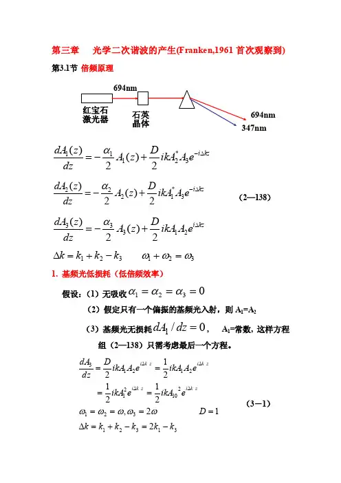
第三章 光学二次谐波的产生(Franken,1961首次观察到)第3.1节 倍频原理*11123()()22i kzdA z D A z ikA A e dz α-∆=-+ *22213()()22i kzdA z D A z ikA A e dz α-∆=-+ (2—138) 33312()()22i kzdA z D A z ikA A e dz α∆=-+ 321k k k k -+=∆ 321ωωω=+1. 基频光低损耗(低倍频效率) 假设:(1)无吸收0321===ααα(2)假定只有一个偏振的基频光入射,则A 1=A 2 (3)基频光无损耗0/1=dzdA , A 1=常数, 这样方程组(2—138)只需考虑最后一个方程。
313213212102121213212,2121212k k k k k k D e ikA e ikA e A ikA e A ikA D dz dA z k i z k i zk i z k i -=-+=∆========∆∆∆∆ωωωωω(3-1)利用边界条件)1(2121)(0,02102103033-∆====∆∆==⎰kl i lkz i z z e k kA dz e ikA z A A E (3—2)因为光强ϕεcos 220E nc I = (3—3)(因1cos ,1cos =故以后就都取ϕϕ≈)又 202)3,2,1(mm mmmm A c I m A n E ωεω=∴==(3—4)所以22202230233031))(()(412)(2)(-∆⋅==∆kLi e l A k k c l A c l I ωεωε (3—5)321321222321321n n cd k n n n cd k eff eff ωωωωω==(3—6) 又[][])2(sin 4)cos(1214)cos(12)cos(22122kl kl kl kl ekLi ∆=∆-⋅=∆-=∆-=-∆22222103210321222410321032122120222241032132122303)2()2(sin 2)2()2(sin 42)2()2(sin 42)(kl kl d l I n n c l kl kl A n n c d c l kl kl A n n c d c l I eff eff eff ∆∆=∆∆=∆∆=∴εωεωωεωωωε (3—7) 若改用功率来表示,则有S P I /=于是22212232103213)2()2(sin 2)(kl kl S P d l n n c l P eff∆∆=∴εω (3—8)定义倍频效率2210223210321113)2()2(sin 2)()2(kl klI d l n n c P P eff ∆∆==εωωωη (3—9)讨论:(1)2103)(I l I ∝ (3—10)(2)⎪⎩⎪⎨⎧∝2210ld I eff η (3—11)22/)(sin )(x x x f =(3)22)2()2(sin kl kl ∆∆∝η,(当1,0这个因子==∆k )(3—11) (4)如果,0=∆k (相位匹配),则有2l ∝η,但实际上还有许多因素,需要考虑。

二次谐波产生过程嘿,朋友们!今天咱来聊聊二次谐波产生过程这个神奇的玩意儿。
你说这二次谐波产生过程啊,就好像一场奇妙的音乐演奏会!咱先把激光束想象成一群有活力的小乐手,它们雄赳赳气昂昂地往前冲。
当这些小乐手们碰到特定的材料时,就像是来到了一个特别的舞台。
在这个舞台上,小乐手们开始展现它们独特的魅力。
它们相互作用,就像乐手们之间的默契配合一样。
然后呢,神奇的事情发生啦!原本单一频率的激光束,突然就产生了新的频率,这可不就是像原本演奏一首曲子的乐手们突然奏出了全新的旋律嘛!你想想看,这多有意思啊!就好比你本来只期待听到一种声音,结果却给你来个惊喜,多了一种更美妙的声音。
而且啊,这二次谐波产生过程还特别挑呢!不是随便什么材料都能让它完美展现的,这就跟好的乐手也得挑个好舞台是一个道理。
它就像是一个隐藏在科学世界里的小魔法,等着我们去发现和探索。
要是你不去了解它,那可就太可惜啦!你难道不想知道这神奇的小魔法是怎么施展的吗?咱再深入一点说,这二次谐波产生过程对于很多领域那可都是大功臣啊!在医学上,它能帮助医生更清楚地看到我们身体里的情况,就像给医生配上了一副超级厉害的眼镜。
在通信领域呢,它能让信号传输得更稳定、更高效,就像给通信搭起了一条顺畅的高速公路。
哎呀呀,这二次谐波产生过程真的是太重要啦!它就像一个默默无闻却超级厉害的幕后英雄,为我们的生活带来了那么多的便利和进步。
所以啊,朋友们,可别小瞧了这看似深奥的二次谐波产生过程。
它虽然藏在科学的海洋里,但只要我们用心去了解,就会发现它的魅力和价值简直无穷无尽!我们得好好感谢那些研究它的科学家们,是他们让我们有机会领略到这神奇的世界。
怎么样,现在是不是对二次谐波产生过程更感兴趣啦?那就赶紧去探索吧!原创不易,请尊重原创,谢谢!。


§2.3 二次谐波的产生及其解二次谐波或倍频是一种很重要二阶非线性光学效应,在实践中有广泛的应用,如Nd:YAG 激光器的基频光(1.064μm)倍频成0.532μm 绿光,或继续将0.532μm 激光倍频到0.266μm 紫外区域。
本节从二阶非线性耦合波方程出发,求解出产生的二次谐波光强小信号解,并解释相位匹配对二次谐波产生的影响。
2.3.1 二次谐波的产生设基频波的频率为1ω,复振幅为1E ;二次谐波的频率为()2212ωωω=,复振幅2E 。
由基频波在介质中极化产生的二阶极化强度()2P ,辐射出的二次谐波场()3E z 所满足的非线性极化耦合波方程()()()222202222ik z d E z i P z e dz k μω-= (2.3.1-1) ()()()()()1222110211;,ik z P z z E z e εχωωω=-:E (2.3.1-2)注意简并度1D =,212ωω=()()()()()()()()()22202110211221112112;,2;,i kzi kzd E z i E z E ze dz k iE z E z e n cμωεχωωωωχωωω∆∆=-:=-: (2.3.1-3)波矢失配量, 122k k k ∆=- (2.3.1-4) 写成单位矢量(光波的偏振方向或电场的振动方向)和标量的乘积形式333E a E =,基频光场可能有两种偏振方向,即'1111,a E a E ,两种偏振方向可以是相互平行也可以是相互垂直,并有331a a ⋅=()()()()'222121121112;,i kz dE z i a a a E z e dz n c ωχωωω∆⎡⎤=⋅-::⎢⎥⎣⎦ (2.3.1-5)基频波与产生的二次谐波耦合产生的极化场强度()21P ,辐射出基频光场满足的非线性极化耦合波方程。
()()()122101112ik z d E z i P z e dz k μω-= (2.3.1-6)()()()()()21*2()12101212;,i k k z P z z E z e εχωωω-=--:E (2.3.1-7)()()()()()'21*1121121211;,::i kz dE z i a a a z E z e dz n c ωχωωω-∆⎡⎤=⋅--E ⎢⎥⎣⎦ (2.3.1-8)如果介质对频率为13,ωω的光波都是无耗的,即13,ωω远离共振区,则()()()()22311131;,,;,χωωωχωωω---都是实数。
精心整理精心整理倍频现象的理论解释线性光学效应的特点:出射光强与入射光强成正比;不同频率的光波之间没有相互作用,没有相互作用包括不能交换能量;效应来源于介质中与作用光场成正比的线性极化。
非线性光学效应的特点:出射光强不与入射光强成正比(例如成平方或者三次方的关系);不同频率光波之间存在相互作用,可以交换能量;效应来源于介质中与作用光场不成正比的非线性极化。
倍频效应是非线性的光学效应,当介质在光波电场的作用下时,会产生极化。
设P 是光场E 在介质中产生的极化强度。
对于线性光学过程:P=对于非线性光学过程:P 可以展开为E 的幂级数:其中:,…,n 阶非线性极化强度。
为n 阶极化率。
正是这些非线性极化项的出现,度所导致产生的: 设光场是频率为、波矢为的单色波,即:则中将出现项: 该极化项的出现,可以看作介质中存在频率为的振荡电偶极矩,的倍频光。
介质产生非线性极化:从微观上看,非线性是由原子、分子非谐性所造成的。
物质受强光作用后,电子发生位移x ,具有位能V(x)+x 和-x 相对应的位能并不相等,即:V(+X)≠V(-x),因而位能函数V(x)应该包含奇次项:当D 时,正位移引起的恢复力大于负位移引起的恢复力。
如果作用在电子上的电场力是正的,则会引起一个相对较小的位移;反之,则会引起一个相对较大的位移。
那么,电场正方向产生的极化强度就比电场反方向产生的极化强度小。
这就使得非线性极化的产生。
有了非线性极化,那么,一个给定的强光波电场对应的极化波就是一个正峰值b 比负峰值b ’小的非线性极化波:而根据傅里叶分析,任何一个非正弦的周期函数,都可以分解成角频率为、2、3、…的正弦波。
所以强光波电场在介质中引起的非线性极化波,可以分解成为角频率为的基频极化波,角频率为的二次谐频极化波,以及常值分量等成分。
而其中角频率为2的二次谐波,就是倍频光。
倍频转换效率:在发现倍频效应初期,产生二次谐波的效率是非常低的约为数量级。