JQX-115F-T0601HNil3A中文资料
- 格式:pdf
- 大小:216.82 KB
- 文档页数:2

KORYfYJRJJLJLRKMJ86++/6YZ*5FaE=-IE h =1o cn @_2K B n H n @`<a h _Z n B W T u pN Y \:;>Z d h j \o cn @`5E h =BKC Ug `r x ^\`>BLC a +Vs}6a J5D;9I3;9KLW LQQkWYKIL^e LOJkWY KIM^e KLOkWY KLWI LQQkWYXMJJ gMJJKLW LQQkWY KPW LQQ kWY SW LOJkWY KJO}YK^e LOJkWY KIL^e KLOkWY ikGO KLOkWYK 4L :BWqYodCK 4L :BWqhud L C M :BWqYodCK 4L :BWqcrCKOSN :BWqYodCM :BWqhud L CM :BWqcrCN :BWqhud L C N :BWqcrCKPW LQQ kWY KIM^e KLOkWYKIL^e LOJkWYXMJJ gMJJKPW LQQkWYO\aWF MJagW LOJkWYKJW LOJkWY RW LQQkWY KIL^e LOJkWY KIN^e KLOkWYRW LQQkWY RW LQQkWYw LM`E h =F U i 0_.2T ?Q \hN ,m :1V <R >.f 4.F y 2G R ~k+-5KPJB^\KKO\I u u u G u u G u GK G u u CMHOIOttF K n F KLWF ^\KKO\I u u u GK u G u GKILG u uOttF K n F KPWF ^\KKO\I u u u GK u G u GMG u uOttF L n F RWF ^\KKO\I u u u GL u G u GNG u uMHOtt I _c\p Ott I _c\p B^\KKO\I uuu G uu G u G LIMIN G uu C/k bs 0.:x <PCT[S>XS Dn U s Dni LDn UHDn U s Dni LDn UH,n U s ,ni L,n UHT[S t >XS tw bB |~d z T ttE h BKC W elKk :M C ^L h 4hd L 4cd L 4-Xi *O +;/[N Y <t ][N ~DW :T ?>W*O Kk :C D o -h ^L h 4hd L 4cd L 4-Xi *O +;/[N Y <`G?N l /:T ?<L G W Z Y [Ne j <NQ >f Z n B j S eYX A H <R >j <[pE ,<G R ~k+-NQ <F I o <F `hT ?5BLC w Q r h `lz A <o71V x KJtW OkZY 5KKJJKPKw bB |~/k bs 0o c D L;5n 9m =I 22K :p {s I 2BZYC D`l n 4B W Cq p a h B y K J J J J a 02K n @B j I j u C`ln @BkC s v ;5BskWC Kk {s BRO vYCE h 3BKC T ?N ,u ;\b y h \b =S<f u ;\b7Ktt <=S x 6JHLtt >f u ;\b W BK {OCtt _\Y <=S x 6JHMtt >f u ;\b?Ott <=S x 6JHNtt >BLC @j w \b e y h \b =S x 6JHKtt >BMC v 6x s x LHOLtt 5KHJJHPENJ EKJJERJ EPJ LHL KHR KHNLHP MHJ MHN MHP ERO NG vGT ?@6e i<vI [N Y P t <T P 93<i M 2<r ^5w G {z A <M u ;@o Z n B W 77o p KN 1S h n P=;P h B H <H z vI K 8no p h [N q _?YR_3>=hT ?<T PE }<G R G {+-F IO J 9xh V f ][5eT ??:XP i O vI1X 5|08G {n V ?.P1=k BLn P <G =k C 3n P L }5\HJXSMHOtt K n KLWOtt K nKPWOtt K n KLWOtt L n RWT[S t >XS tw bB |~d z T ttE h =1Z n B[N B Y e <R AS|n @W B yon @aN g b Z n B n 9m =b j5W t ]n @|w:<wn 9m =h L5N 7D85W B s e I 2@oh U 1`<Z n B 2K h q TP u ;N F m J 5KJOJKJJLJJOJJLJMJ NJ MJJ NJJ。
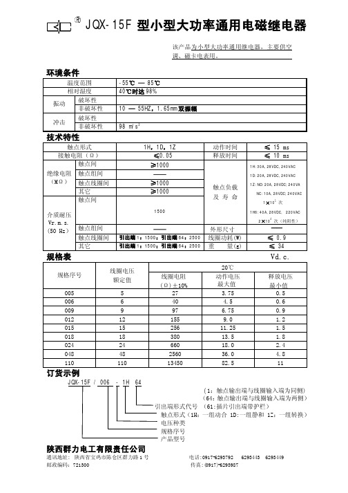

JQX-15F小型大功率电磁继电器触点切换电流可达30A;触点切换功率高达7500VA;标准PCB式引出端,封闭式; 认证:CQC 03001003921,UL E205607,CE;同类型号:T90。
温度范围相对湿度大气压力工作位置-25℃+55℃~+40℃达90%86kPa 106kPa ~任意使用条件触点形式初始接触电阻触点材料触点负载(阻性)最大开关电压最大开关电流最大切换功率电气寿命(次)机械寿命(次)1H(A)、1Z(C)100mΩ银合金1H:30A;1Z:20A(250VAC/28VDC)250VAC/125VDC 1H:30A;1Z:20A1H:7500VA/840W;1Z:5000VA/560W 51×1071×103.1 触点参数1适用范围2正常工作条件和安装条件3主要参数及技术性能绝缘电阻介质耐压动作时间释放时间冲击(稳定性)振动引出端形式外形尺寸(mm)触点线圈间断开触点间100MΩ(500VDC)2000VAC 1500VAC ≤25ms ≤25ms2加速度100m/s ,脉冲持续时间11ms 双振幅1.5mm,1055Hz ~PCB32.5×27.5×20.53.2 性能、特征参数3.3 线圈参数3.4 规格参数额定功耗吸合电压释放电压最大电压0.93W ≤75%额定电压≥10%额定电压110%额定电压额定电压VDC 5691218243648动作电压VDC(≤)3.84.56.89.013.518.027.036.0释放电压VDC(≥)0.50.60.91.21.82.43.64.8线圈电阻(20℃)Ω±10%27398715534861913942477C4外形及安装尺寸底视接线图(1Z、1Z1)底视接线图(1H、1H1)1Z、1Z1安装孔位图(底视图)1H、1H1安装孔位图(底视图)外形图1Z:一组转换1H:一组动合直流548V~无:敞开式1:有3号引出脚无:无3号引出脚订货须知5。


Distributor: Electro-Stock Tel: 630-682-1542 Fax: 630-682-1562 FEATURES:• UL F class rated standard• Small size and light weight, low coil power consumption • Heavy contact load, strong shock and vibration resistance • UL/CUL certifiedE19785226.9 x 31.7 x 20.3 mmCONTACT DATAContact Arrangement 1A = SPST N.O. 1B = SPST N.C. 1C = SPDTContact RatingN.O. 40A @ 240VAC resistive; 30A @ 277VAC General Purpose 2 hp @ 250VACN.C. 30A @ 240VAC resistive, 30VDC; 20A @ 277VAC General Purpose 1-1/2 hp @ 250VAC Contact Resistance < 30 milliohms initial Contact MaterialAgSnO 2, AgSnO 2I n 2O 3 Maximum Switching Power 9600VA, 1120W Maximum Switching Voltage 277VAC, 110VDC Maximum Switching Current 40ACOIL DATACoil VoltageVDCCoil ResistanceΩ ± 10%Rated Max. 0.6W 0.9W Pick Up Voltage VDC (max)75%of rated voltageRelease Voltage VDC (min)10%of rated voltageCoil PowerWOperate TimemsRelease Timems3 3.9 15 10 2.25 0.3 5 6.5 42 28 3.75 0.5 6 7.8 60 40 4.50 0.6 9 11.7 135 90 6.75 0.9 12 15.6 240 160 9.00 1.2 15 19.5 375 250 10.25 1.5 18 23.4 540 360 13.50 1.8 24 31.2 960 640 18.002.4 48 62.4 3840 2560 36.00 4.8 110 140.3 20167 13445 82.50 11.0.60 .9015 10AC COIL PARAMETERSCoil VoltageVACRated Max.Coil ResistanceΩ ± 10%Pick Up Voltage VAC (max)75%of rated voltageRelease Voltage VAC (min)30%of rated voltageCoil PowerVAOperate TimemsRelease Timems12 15.6 27 9.0 3.6 24 31.2 120 18.0 7.2 110 143 2360 82.5 33 120 156 3040 90 36 220 286 13490 165 66 240 312 15320 180 72 277 360 20210 207 83.12VA 15 10Distributor: Electro-Stock Tel: 630-682-1542 Fax: 630-682-1562 GENERAL DATAElectrical Life @ rated load Mechanical Life 100K cycles, typical 10M cycles, typicalInsulation Resistance 100MΩ min @ 500VDCDielectric Strength, Coil to Contact Contact to Contact 4000V rms min. @ sea level (With Pin 6 removed) 2500V rms min. @ sea level (With Pin 6)1500V rms min. @ sea levelShock Resistance 200m/s2 for 11msVibration Resistance 1.50mm double amplitude 10-40Hz Terminal (Copper Alloy) Strength 10NOperating Temperature Storage Temperature -55 °C to + 125 °C -55 °C to + 155 °CSolderability 230 °C ± 2 °C for 10 ± 0.5sWeight 30g, 27g (no cover)ORDERING INFORMATION1. Series:WJ115F1WJ115F12. Contact Arrangement:1A = SPST N.O.1B = SPST N.C.1C = SPDT1C4. Coil Voltage:3VDC5VDC6VDC9VDC12VDC15VDC18VDC24VDC48VDC110VDC12VAC24VAC110VAC120VAC220VAC240VAC277VAC12VDC S5. Sealing Options:S = Sealed (standard)N = No cover66.Option:None = Pin 6 Included6 = Pin 6 Removed.67.Coil Power:.9 = .9W.6 = .6WBlank = 2VA (AC Coil)8.Contact Material:Blank = AgSnO2U = AgSnO2I n2O3Distributor: Electro-Stock Tel: 630-682-1542 Fax: 630-682-1562DIMENSIONS (Units = mm)S = SEALEDN = NO COVERSCHEMATICS & PC LAYOUTS (BOTTOM VIEWS)1A 1B 1CWITH PIN 6WITHOUT PIN 6。

HCPL-0601中⽂资料CAUTION: The small device geometries inherent to the design of this bipolar component increase the component's susceptibility to damage from electrostatic discharge (ESD). It is advised that normal static precautions be taken in handling and assembly of this component to prevent damage and/or degradation which may be induced by ESD.Small Outline, 5 Lead, High CMR, High Speed, Logic Gate Optocouplers Technical DataHCPL-M600HCPL-M601HCPL-M611DescriptionThese small outline high CMR,high speed, logic gate optocoup-lers are single channel devices in a five lead miniature footprint.They are electrically equivalent to the following Agilentoptocouplers (except there is no output enable feature):SO-5 Package Standard DIP SO-8 Package HCPL-M6006N137HCPL-0600HCPL-M601HCPL-2601HCPL-0601HCPL-M611HCPL-2611HCPL-0611The SO-5 JEDEC registered (MO-155) package outline does not require “through holes” in a PCB.This package occupies approximately one fourth the footprint area of the standard dual-in-line package. The lead profile is designed to be com-patible with standard surface mount processes.The HCPL-M600/01/11 optically coupled gates combine a GaAsP light emitting diode and an integrated high gain photon detector. The output of thedetector I.C. is an Open-collectorSchottky-clamped transistor. The internal shield provides a guaranteed common modetransient immunity specification of 5,000 V/µs for the HCPL-M601,and 10,000 V/µs for the HCPL-M611.This unique design provides maximum ac and dc circuit isolation while achieving TTL compatibility. The optocoupler ac and dc operational parameters are guaranteed from -40°C to 85°C allowing trouble free system performance.FeaturesSurface MountableVery Small, Low Profile JEDEC Registered Package OutlineCompatible with Infrared Vapor Phase Reflow and Wave Soldering Processes Internal Shield for High Common Mode Rejection (CMR)HCPL-M601: 10,000 V/µs at V CM = 50 VHCPL-M611: 15,000 V/µs at V CM = 1000 VHigh Speed: 10 Mbd LSTTL/TTL Compatible Low Input Current Capability: 5 mAGuaranteed ac and dc Performance overTemperature: -40°C to 85°C ? Recognized under theComponent Program of U.L.(File No. E55361) forDielectric Withstand Proof Test Voltage of 2500 Vac, 1MinuteThe HCPL-M600/01/11 are suitable for high speed logic interfacing, input/outputbuffering, as line receivers in environments that conventionalline receivers cannot tolerate, and are recommended for use inextremely high ground or induced noise environments.Outline Drawing (JEDEC MO-155)ApplicationsIsolated Line Receiver Simplex/Multiplex Data TransmissionComputer-Peripheral InterfaceMicroprocessor System InterfaceDigital Isolation for A/D, D/A ConversionSwitching Power Supply Instrument Input/Output IsolationGround Loop Elimination Pulse Transformer ReplacementPin Location (for reference only)SchematicUSE OF A 0.1 µF BYPASS CAPACITOR MUST BE CONNECTED BETWEEN PINS 6 AND 4 (SEE NOTE 1). V CC V OGNDTRUTH TABLE (POSITIVE LOGIC)LEDONOFFOUTPUT L H65431V CCV OUT GNDANODE 0.71 (0.028)UNDERSIDE OF THE PACKAGEDIMENSIONS IN MILLIMETERS (INCHES) * MAXIMUM MOLD FLASH ON EACH SIDE IS 0.15 mm (0.006) Recommended Operating ConditionsParameterSymbol Min.Max.Units Input Current, Low Level I FL *0250µA Input Current, High Level I FH 515m A Supply Voltage, Output V CC 4.55.5V Fan Out (R L = 1 k ?)N 5TTLLoads Output Pull-Up Resistor R L 3304,000?Operating TemperatureT A-4085°C* The off condition can also be guaranteed by ensuring that V F (off) ≤ 0.8 volts.Absolute Maximum Ratings(No Derating Required up to 85°C)Storage Temperature....................................................-55°C to +125°C Operating Temperature ..................................................-40°C to +85°C Forward Input Current - I F (see Note 2).......................................20 mA Reverse Input Voltage - V R .................................................................5 V Supply Voltage - V CC (1 Minute Maximum)........................................7 V Output Collector Current - I O ........................................................50 mA Output Collector Power Dissipation .. (85)mW Output Collector Voltage - V O ............................................................7 V (Selection for higher output voltages up to 20 V is available)Infrared and Vapor Phase Reflow Temperature.......................see belowMaximum Solder Reflow Thermal Profile.(Note: Use of Non-Chlorine Activated Fluxes is Recommended.)240TIME – MINUTEST E M P E R A T U R E – °C220200180160140120100806040200260Insulation Related SpecificationsParameter Symbol Value Units ConditionsMin. External Air Gap L(IO1)≥5mm Measured from input terminals (Clearance)to output terminalsMin. External Tracking Path L(IO2)≥5mm Measured from input terminals (Creepage)to output terminalsMin. Internal Plastic Gap0.08mm Through insulation distance (Clearance)conductor to conductor Tracking Resistance CTI175V DIN IEC 112/VDE 0303 Part 1 Isolation Group (per DIN VDE 0109)IIIa Material Group DIN VDE 0109 Electrical SpecificationsOver recommended temperature (T A = -40°C to 85°C) unless otherwise specified. (See note 1.)*All typicals at T A = 25°C, V CC = 5 V.Switching SpecificationsOver recommended temperature (T A = -40°C to 85°C), V CC = 5 V, I F = 7.5 mA unless otherwise specified.*All typicals at T A = 25°C, V CC = 5 V.Notes:1. Bypassing of the power supply line is required with a 0.1 µF ceramic disc capacitor adjacent to each optocoupler. The total leadlength between both ends of the capacitor and the isolator pins should not exceed 10mm.2. Peaking circuits may produce transient input currents up to 50 mA, 50 ns maximum pulse width, provided average current does not exceed 20mA.3. Device considered a two terminal device: pins 1 and 3 shorted together, and pins 4, 5 and 6 shorted together.4. In accordance with UL 1577, each optocoupler is proof tested by applying an insulation test voltage ≥3000 V RMS for 1 second(Leakage detection current limit, I I-O≤ 5 µA).5. The t PLH propagation delay is measured from 3.75 mA point on the falling edge of the input pulse to the 1.5 V point on the rising edge of the output pulse.6. The t PHL propagation delay is measured from 3.75 mA point on the rising edge of the input pulse to the 1.5 V point on the falling edge of the output pulse.7. CM H is the maximum tolerable rate of rise of the common mode voltage to assure that the output will remain in a high logicstate (i.e., V OUT > 2.0V).8. CM L is the maximum tolerable rate of fall of the common mode voltage to assure that the output will remain in a low logic state (i.e., V OUT > 0.8 V).9. For sinusoidal voltages, (|dV CM|/dt)max = πf CM V CM(p-p).10. See application section; “Propagation Delay, Pulse-Width Distortion and Propagation Delay Skew” for more information.11. t PSK is equal to the worst case difference in t PHL and/or t PLH that will be seen between units at any given temperature withinthe worst case operating condition range.Figure 5. Low Level Output Current vs. Temperature.Figure 4. Output Voltage vs.Forward Input current.Figure 1. High Level Output Current vs. Temperature.Figure 2. Low Level Output Voltage vs. Temperature.Figure 3. Input Diode Forward Characteristic.Figure 6. Test Circuit for t PHL and t PLH .I O H – H I G H L E V E L O U T P U T C U R R E N T – µAT A – TEMPERATURE – °C101550.4T A – TEMPERATURE – °C 0.30.1V O L – L O W L E V E L O U T P U T V O L T A G E – V0.2V F – FORWARD VOLTAGE – VOLTS10I F – F O R W A R D C U R R E N T – m A100I F – FORWARD INPUT CURRENT – mAV O – O U T P U TV O L T A G E – VI O L – L O W L E V E L O U T P U T C U R R E N T – m A T A – TEMPERATURE – °C60802040OUTPUT V O MONITORING NODEI FV F = 7.5 mAF = 3.75 mAFigure 12. Temperature Coefficient for Forward Voltage vs. Input Current.Figure 10. Rise and Fall Time vs.Temperature.Figure 9. Pulse Width Distortion vs.Temperature.Figure 8. Propagation Delay vs.Pulse Input Current.Figure 7. Propagation Delay vs.Temperature.Figure 11. Test Circuit for Common Mode Transient Immunity and Typical Waveforms.10080T A – TEMPERATURE – °C 600t P – P R O P A G A T I O N D E L A Y – n s402010590I F – PULSE INPUT CURRENT – mA7530t P – P R O P A G A T I O N D E L A Y – n s60454030T A – TEMPERATURE – °C20P W D – P U L S E W I D T H D I S T O R T I O N – n s10-10t r , t f– R I S E , F A L L T I M E – n sT A – TEMPERATURE – °Cd V F /d T – F O R W A R D V O L T A G E T E M P E R A T U R E C O E F F I C I E N T – m V /°C0.1110100I F – PULSE INPUT CURRENT – mA-1.4-2.2-2.0-1.8-1.6-1.2-2.4V O 0.5 VV O (MIN.)5 V0 V SWITCH AT A: I F = 0 mA SWITCH AT B: I F = 7.5 mAV CMCM HCM LV O (MAX.)V CM (PEAK)V O+5 VO GENERATOR Z O = 50 ?Propagation Delay, Pulse-Width Distortion and Propagation Delay Skew Propagation delay is a figure of merit which describes how quickly a logic signal propagates through a system. The propaga-tion delay from low to high (t PLH) is the amount of time required for an input signal to propagate to the output, causing the output to change from low to high. Similarly, the propagation delay from high to low (t PHL) is the amount of time required for the input signal to propagate to the output, causing the output to change from high to low (see Figure 7).Pulse-width distortion (PWD) results when t PLH and t PHL d iffer in value. PWD is defined as the difference between t PLH and t PHL and often determines the maxi-mum data rate capability of a transmission system. PWD can be expressed in percent by dividing the PWD (in ns) by the minimum pulse width (in ns) being transmitted. Typically, PWD on the order of 20-30% of the minimum pulse width is tolerable; the exact figure depends on the particular application (RS232,RS422, T-1, etc.).Propagation delay skew, t PSK, is an important parameter to consider in parallel data appli-cations where synchronization of signals on parallel data lines is a concern. If the parallel data is being sent through a group ofoptocouplers, differences inpropagation delays will cause thedata to arrive at the outputs of theoptocouplers at different times. Ifthis difference in propagationdelays is large enough, it willdetermine the maximum rate atwhich parallel data can be sentthrough the optocouplers.Propagation delay skew is definedas the difference between theminimum and maximumpropagation delays, either t PLH ort PHL, for any given group ofoptocouplers which are operatingunder the same conditions (i.e.,the same drive current, supplyvoltage, output load, andoperating temperature). Asillustrated in Figure 15, if theinputs of a group of optocouplers are switched either ON or OFF at the same time, t PSK is the difference between the shortest propagation delay, either t PLH or t PHL, and the longest propagation delay, either t PLH or t PHL.As mentioned earlier, t PSK can determine the maximum parallel data transmission rate. Figure 11 is the timing diagram of a typical parallel data application with both the clock and the data lines being sent through optocouplers. The figure shows data and clock signals at the inputs and outputs of the optocouplers. To obtain the maximum data transmission rate, both edges of the clock signal are being used to clock the data; if only one edge were used, the clock signal would need to be twice as fast.Propagation delay skew represents the uncertainty of where an edge might be after being sent through an optocoupler. Figure 16 shows that there will be uncertainty in both the data and the clock lines. It is important that these two areas of uncertainty not overlap, otherwise the clock signal might arrive before all of the data outputs have settled, or some ofthe data outputs may start tochange before the clock signalhas arrived. From theseconsiderations, the absoluteminimum pulse width that can besent through optocouplers in aparallel application is twice t PSK. Acautious design should use aslightly longer pulse width toensure that any additionaluncertainty in the rest of thecircuit does not cause a problem.The t PSK specified optocouplersoffer the advantages ofguaranteed specifications forpropagation delays, pulse-widthdistortion and propagation delayskew over the recommendedtemperature, and input current,and power supply ranges.Figure 15. Illustration ofPropagation Delay Skew – t PSK .Figure 13. Input Threshold Current vs. Temperature.Figure 14. Recommended TTL/LSTTL to TTL/LSTTL Interface Circuit. Figure 16. Parallel Data Transmission Example.I T H – I N P U T T H R E S H O L D C U R R E N T – m AT A – TEMPERATURE – °C452316V* DIODE D1 (1N916 OR EQUIVALENT) IS NOT REQUIRED FOR UNITS WITH OPEN COLLECTOR OUTPUT. CC 2I FV OI FV ODATAINPUTS CLOCKDATAOUTPUTSCLOCK/doc/9b0bff6d783e0912a2162a2e.html Data subject to change.Copyright ? 1999 Agilent Technologies Obsoletes 5091-9635E (10/93)5966-4942E (11/99)。

Distributor: Electro-Stock Tel: 630-682-1542 Fax: 630-682-1562 FEATURES:• UL F class rated standard• Small size and light weight, low coil power consumption • Heavy contact load, strong shock and vibration resistance • UL/CUL certifiedE19785226.9 x 31.7 x 20.3 mmCONTACT DATAContact Arrangement 1A = SPST N.O. 1B = SPST N.C. 1C = SPDTContact RatingN.O. 40A @ 240VAC resistive; 30A @ 277VAC General Purpose 2 hp @ 250VACN.C. 30A @ 240VAC resistive, 30VDC; 20A @ 277VAC General Purpose 1-1/2 hp @ 250VAC Contact Resistance < 30 milliohms initial Contact MaterialAgSnO 2, AgSnO 2I n 2O 3 Maximum Switching Power 9600VA, 1120W Maximum Switching Voltage 277VAC, 110VDC Maximum Switching Current 40ACOIL DATACoil VoltageVDCCoil ResistanceΩ ± 10%Rated Max. 0.6W 0.9W Pick Up Voltage VDC (max)75%of rated voltageRelease Voltage VDC (min)10%of rated voltageCoil PowerWOperate TimemsRelease Timems3 3.9 15 10 2.25 0.3 5 6.5 42 28 3.75 0.5 6 7.8 60 40 4.50 0.6 9 11.7 135 90 6.75 0.9 12 15.6 240 160 9.00 1.2 15 19.5 375 250 10.25 1.5 18 23.4 540 360 13.50 1.8 24 31.2 960 640 18.002.4 48 62.4 3840 2560 36.00 4.8 110 140.3 20167 13445 82.50 11.0.60 .9015 10AC COIL PARAMETERSCoil VoltageVACRated Max.Coil ResistanceΩ ± 10%Pick Up Voltage VAC (max)75%of rated voltageRelease Voltage VAC (min)30%of rated voltageCoil PowerVAOperate TimemsRelease Timems12 15.6 27 9.0 3.6 24 31.2 120 18.0 7.2 110 143 2360 82.5 33 120 156 3040 90 36 220 286 13490 165 66 240 312 15320 180 72 277 360 20210 207 83.12VA 15 10Distributor: Electro-Stock Tel: 630-682-1542 Fax: 630-682-1562 GENERAL DATAElectrical Life @ rated load Mechanical Life 100K cycles, typical 10M cycles, typicalInsulation Resistance 100MΩ min @ 500VDCDielectric Strength, Coil to Contact Contact to Contact 4000V rms min. @ sea level (With Pin 6 removed) 2500V rms min. @ sea level (With Pin 6)1500V rms min. @ sea levelShock Resistance 200m/s2 for 11msVibration Resistance 1.50mm double amplitude 10-40Hz Terminal (Copper Alloy) Strength 10NOperating Temperature Storage Temperature -55 °C to + 125 °C -55 °C to + 155 °CSolderability 230 °C ± 2 °C for 10 ± 0.5sWeight 30g, 27g (no cover)ORDERING INFORMATION1. Series:WJ115F1WJ115F12. Contact Arrangement:1A = SPST N.O.1B = SPST N.C.1C = SPDT1C4. Coil Voltage:3VDC5VDC6VDC9VDC12VDC15VDC18VDC24VDC48VDC110VDC12VAC24VAC110VAC120VAC220VAC240VAC277VAC12VDC S5. Sealing Options:S = Sealed (standard)N = No cover66.Option:None = Pin 6 Included6 = Pin 6 Removed.67.Coil Power:.9 = .9W.6 = .6WBlank = 2VA (AC Coil)8.Contact Material:Blank = AgSnO2U = AgSnO2I n2O3Distributor: Electro-Stock Tel: 630-682-1542 Fax: 630-682-1562DIMENSIONS (Units = mm)S = SEALEDN = NO COVERSCHEMATICS & PC LAYOUTS (BOTTOM VIEWS)1A 1B 1CWITH PIN 6WITHOUT PIN 6。

Distributor: Electro-Stock Tel: 630-682-1542 Fax: 630-682-1562 FEATURES:• UL F class rated standard• Small size and light weight, low coil power consumption • Heavy contact load, strong shock and vibration resistance • UL/CUL certifiedE19785226.9 x 31.7 x 20.3 mmCONTACT DATAContact Arrangement 1A = SPST N.O. 1B = SPST N.C. 1C = SPDTContact RatingN.O. 40A @ 240VAC resistive; 30A @ 277VAC General Purpose 2 hp @ 250VACN.C. 30A @ 240VAC resistive, 30VDC; 20A @ 277VAC General Purpose 1-1/2 hp @ 250VAC Contact Resistance < 30 milliohms initial Contact MaterialAgSnO 2, AgSnO 2I n 2O 3 Maximum Switching Power 9600VA, 1120W Maximum Switching Voltage 277VAC, 110VDC Maximum Switching Current 40ACOIL DATACoil VoltageVDCCoil ResistanceΩ ± 10%Rated Max. 0.6W 0.9W Pick Up Voltage VDC (max)75%of rated voltageRelease Voltage VDC (min)10%of rated voltageCoil PowerWOperate TimemsRelease Timems3 3.9 15 10 2.25 0.3 5 6.5 42 28 3.75 0.5 6 7.8 60 40 4.50 0.6 9 11.7 135 90 6.75 0.9 12 15.6 240 160 9.00 1.2 15 19.5 375 250 10.25 1.5 18 23.4 540 360 13.50 1.8 24 31.2 960 640 18.002.4 48 62.4 3840 2560 36.00 4.8 110 140.3 20167 13445 82.50 11.0.60 .9015 10AC COIL PARAMETERSCoil VoltageVACRated Max.Coil ResistanceΩ ± 10%Pick Up Voltage VAC (max)75%of rated voltageRelease Voltage VAC (min)30%of rated voltageCoil PowerVAOperate TimemsRelease Timems12 15.6 27 9.0 3.6 24 31.2 120 18.0 7.2 110 143 2360 82.5 33 120 156 3040 90 36 220 286 13490 165 66 240 312 15320 180 72 277 360 20210 207 83.12VA 15 10Distributor: Electro-Stock Tel: 630-682-1542 Fax: 630-682-1562 GENERAL DATAElectrical Life @ rated load Mechanical Life 100K cycles, typical 10M cycles, typicalInsulation Resistance 100MΩ min @ 500VDCDielectric Strength, Coil to Contact Contact to Contact 4000V rms min. @ sea level (With Pin 6 removed) 2500V rms min. @ sea level (With Pin 6)1500V rms min. @ sea levelShock Resistance 200m/s2 for 11msVibration Resistance 1.50mm double amplitude 10-40Hz Terminal (Copper Alloy) Strength 10NOperating Temperature Storage Temperature -55 °C to + 125 °C -55 °C to + 155 °CSolderability 230 °C ± 2 °C for 10 ± 0.5sWeight 30g, 27g (no cover)ORDERING INFORMATION1. Series:WJ115F1WJ115F12. Contact Arrangement:1A = SPST N.O.1B = SPST N.C.1C = SPDT1C4. Coil Voltage:3VDC5VDC6VDC9VDC12VDC15VDC18VDC24VDC48VDC110VDC12VAC24VAC110VAC120VAC220VAC240VAC277VAC12VDC S5. Sealing Options:S = Sealed (standard)N = No cover66.Option:None = Pin 6 Included6 = Pin 6 Removed.67.Coil Power:.9 = .9W.6 = .6WBlank = 2VA (AC Coil)8.Contact Material:Blank = AgSnO2U = AgSnO2I n2O3Distributor: Electro-Stock Tel: 630-682-1542 Fax: 630-682-1562DIMENSIONS (Units = mm)S = SEALEDN = NO COVERSCHEMATICS & PC LAYOUTS (BOTTOM VIEWS)1A 1B 1CWITH PIN 6WITHOUT PIN 6。

Distributor: Electro-Stock Tel: 630-682-1542 Fax: 630-682-1562 FEATURES:• UL F class rated standard• Small size and light weight, low coil power consumption • Heavy contact load, strong shock and vibration resistance • UL/CUL certifiedE19785226.9 x 31.7 x 20.3 mmCONTACT DATAContact Arrangement 1A = SPST N.O. 1B = SPST N.C. 1C = SPDTContact RatingN.O. 40A @ 240VAC resistive; 30A @ 277VAC General Purpose 2 hp @ 250VACN.C. 30A @ 240VAC resistive, 30VDC; 20A @ 277VAC General Purpose 1-1/2 hp @ 250VAC Contact Resistance < 30 milliohms initial Contact MaterialAgSnO 2, AgSnO 2I n 2O 3 Maximum Switching Power 9600VA, 1120W Maximum Switching Voltage 277VAC, 110VDC Maximum Switching Current 40ACOIL DATACoil VoltageVDCCoil ResistanceΩ ± 10%Rated Max. 0.6W 0.9W Pick Up Voltage VDC (max)75%of rated voltageRelease Voltage VDC (min)10%of rated voltageCoil PowerWOperate TimemsRelease Timems3 3.9 15 10 2.25 0.3 5 6.5 42 28 3.75 0.5 6 7.8 60 40 4.50 0.6 9 11.7 135 90 6.75 0.9 12 15.6 240 160 9.00 1.2 15 19.5 375 250 10.25 1.5 18 23.4 540 360 13.50 1.8 24 31.2 960 640 18.002.4 48 62.4 3840 2560 36.00 4.8 110 140.3 20167 13445 82.50 11.0.60 .9015 10AC COIL PARAMETERSCoil VoltageVACRated Max.Coil ResistanceΩ ± 10%Pick Up Voltage VAC (max)75%of rated voltageRelease Voltage VAC (min)30%of rated voltageCoil PowerVAOperate TimemsRelease Timems12 15.6 27 9.0 3.6 24 31.2 120 18.0 7.2 110 143 2360 82.5 33 120 156 3040 90 36 220 286 13490 165 66 240 312 15320 180 72 277 360 20210 207 83.12VA 15 10Distributor: Electro-Stock Tel: 630-682-1542 Fax: 630-682-1562 GENERAL DATAElectrical Life @ rated load Mechanical Life 100K cycles, typical 10M cycles, typicalInsulation Resistance 100MΩ min @ 500VDCDielectric Strength, Coil to Contact Contact to Contact 4000V rms min. @ sea level (With Pin 6 removed) 2500V rms min. @ sea level (With Pin 6)1500V rms min. @ sea levelShock Resistance 200m/s2 for 11msVibration Resistance 1.50mm double amplitude 10-40Hz Terminal (Copper Alloy) Strength 10NOperating Temperature Storage Temperature -55 °C to + 125 °C -55 °C to + 155 °CSolderability 230 °C ± 2 °C for 10 ± 0.5sWeight 30g, 27g (no cover)ORDERING INFORMATION1. Series:WJ115F1WJ115F12. Contact Arrangement:1A = SPST N.O.1B = SPST N.C.1C = SPDT1C4. Coil Voltage:3VDC5VDC6VDC9VDC12VDC15VDC18VDC24VDC48VDC110VDC12VAC24VAC110VAC120VAC220VAC240VAC277VAC12VDC S5. Sealing Options:S = Sealed (standard)N = No cover66.Option:None = Pin 6 Included6 = Pin 6 Removed.67.Coil Power:.9 = .9W.6 = .6WBlank = 2VA (AC Coil)8.Contact Material:Blank = AgSnO2U = AgSnO2I n2O3Distributor: Electro-Stock Tel: 630-682-1542 Fax: 630-682-1562DIMENSIONS (Units = mm)S = SEALEDN = NO COVERSCHEMATICS & PC LAYOUTS (BOTTOM VIEWS)1A 1B 1CWITH PIN 6WITHOUT PIN 6。

