基于CD4541B的时间定时器设计
- 格式:pdf
- 大小:149.61 KB
- 文档页数:2

倒计时定时器电路设计倒计时定时器电路是一个常用的电子电路,在各种应用场景中被广泛使用。
例如,在厨房,我们可以使用倒计时定时器电路来实现烹饪定时;在赛车场上,我们可以使用倒计时定时器电路来准确计时比赛时间等等。
下面是一个关于倒计时定时器电路设计的详细说明:首先,我们需要确定时间范围。
根据实际需求,我们可以选择不同的计时范围,如分钟、小时、天等。
不同的时间范围对应着不同的计数器位数,即需要不同数量的计数器。
例如,如果我们需要设计一个分钟级别的倒计时定时器,那么我们需要使用至少6位的计数器,以便表示60分钟。
其次,我们需要确定时间单位。
在设计倒计时定时器电路时,我们需要确定最小的时间单位,即每次计数的时间间隔。
常见的时间间隔有秒、分、时等。
根据实际需求选择最小时间单位。
然后,我们需要选择适当的计数器和显示单元。
计数器是用来计数的关键元件,可以通过不同的计数器实现不同范围和位数的倒计时。
常见的计数器有二进制加法计数器(如74LS191)、二进制表计数器(如74LS193)等。
显示单元可以是数码管,也可以是液晶显示屏等。
接下来,我们需要设计时钟信号源。
时钟信号源可以是晶振电路,也可以是晶振模块,甚至我们可以利用其他电路的时钟来作为时钟信号源。
设计时钟信号源时,需要确定时钟频率,即每秒或每分钟的脉冲数。
根据时钟频率和时间单位选择相应的频率分频电路,以便生成具有所需时间间隔的时钟信号源。
最后,我们需要设计控制逻辑。
控制逻辑用于控制计数器,根据时钟信号源的脉冲将计数器递减。
当计数器减至0时,需要触发警报或其他操作。
控制逻辑可以使用逻辑门、可编程逻辑器件等来实现。
在设计倒计时定时器电路时,还需要考虑一些额外的功能,如暂停、重置、显示等。
这些功能可以通过增加额外的开关、按钮、显示芯片等元件来实现。
总结起来,倒计时定时器电路设计的关键是确定时间范围、时间单位、计数器和显示单元的选择,设计适当的时钟信号源和控制逻辑。
在设计过程中,需要充分考虑实际需求和制约条件,并结合相应的电子元件来实现倒计时定时器电路。
摘要如今的科技已是飞跃的进步,然而定时器的应用永远不会退休。
“定时器”总的来说有两种类型,一种以机械时钟形式的产品,这种定时器功能简单,应用于成本比较低的产品中,如比较古老的滴水计时器、传统的电风扇。
当然滴水计时已被淘汰,而低价的风扇中还是不会淘汰这种机械运转的精度不高的定时器。
另一种是基于电子电路数字技术的新一代产品,这种产品功能强,精度高,控制和使用都比较直观而灵活,是前者的替代之物。
本设计开发了一种基于单片机的专用定时器。
它造价低,功能全,整体性价比高,可适应很多的场合做为保护或定时预警系统中。
此设计是最典型且经典的单片机定时功能应用设计,设计中使用了单片机定时器的设计、单片机中断使用方法、LED显示技术等。
可以实现在100小时内的任意时间定时,另可外控负载和提示报警等。
设计中的硬件电路主要含盖了STC89C51RC单片机、有源蜂鸣器、LED数字显示数码管等。
在硬件的设计基础上,通过软件进行数码管的数值显示、键扫描程序、蜂鸣器的提示音效和报警音效的处理。
关键词:定时器、STC89C51单片机、LED数字显示数码管ABSTRACTToday, technology is a leap of progress, however, the application of the timer never retired. "Timer" In general there are two types, a mechanical clock in the form of products, such a simple timer function, used in low-cost products, such as the old drip timer, traditional fans . Of course, dripping timing has been eliminated, and cheap fan or accuracy of this mechanical operation of the timer will not be eliminated. Another is based on a new generation of electronic circuits digital technology products, this product features high precision, control and use more intuitive and flexible, the former alternative material.The design and development of a microcontroller-based dedicated timer. It is low cost, full-function, and overall cost-effective, and can be adapted to many occasions as a protection or in the timing early warning system.This design is the most typical and classic the microcontroller timing function application design, the design used in the design of a microcontroller timer, microcontroller interrupt usage, LED display technologies. The arbitrary timing can be achieved in 100 hours, another may be outside the control load and prompted alarm.The hardware circuit design covers Microcontroller STC89C51RC active buzzer, LED digital display digital tube. Hardware design based on the value of the digital tube display, key scanner prompt sound and alarm buzzer sound processing through software.Keywords: timer, STC89C51 microcontroller, LED digital display digital tube目录前言 (4)第一章系统任务与总体方案论证 (5)1、设计任务 (5)2、方案论证 (5)3、方案选择 (6)第二章8051单片机的结构 (7)1、8051单片机的特点 (7)2、8051单片机的片内资源 (7)3、8051的引脚信号 (7)4、复位电路 (9)5、时钟电路 (10)第三章LED数码管接口技术 (11)1、LED数码管的结构与原理 (11)2、多位LED显示器的显示方式 (12)3、LED显示器接口技术 (13)第四章多用途定时器装置的硬件设计 (15)1、硬件电路结构 (15)2、电源电路 (15)3、蜂鸣器报警电路 (16)4、系统结构原理整图 (16)5、硬件焊接 (17)第五章多用途定时器装置的软件流程 (19)1、所需要完成的定时器装置功能 (19)2、软件设计思路 (19)3、软件程序流程图 (19)4、多用途定时器装置的源程序如下 (20)5.多用途定时器装置的实际应用 (28)结论 (29)参考文献 (29)致谢 (30)前言含有微处理器、存储器、输入/输出电路及一些诸如中断控制器、定时器/计数器等资源的集成电路芯片,它包含了作为一个计算机所必需的基本部件,在外部只需添加少许的外围器件就可以组成完整的计算机实现控制目的,这样的器件通常称为单片机或微型控制器。

(二 〇 一 二 年 六 月本科毕业设计说明书 题 目:基于单片机的定时器的设计与实现 学生姓名:w w s 学 院:信息工程 系 别:电子信息工程 专 业:电子信息工程 班 级:... 指导教师:...摘要近年来随着计算机在社会领域的渗透和大规模集成电路的发展,单片机的应用正在不断地走向深入,由于它具有功能强,体积小,功耗低,价格便宜,工作可靠,使用方便等特点,因此特别适合于与控制有关的系统,越来越广泛地应用于自动控制,智能化仪器,仪表,数据采集,军工产品以及家用电器等各个领域,单片机往往是作为一个核心部件来使用,在根据具体硬件结构,以及针对具体应用对象特点的软件结合,以作完善。
数子时钟在日常生活中最常见,应用也最广泛。
本次做的数子时钟是以单片机(AT89C51)为核心,结合相关的元器件(时钟芯片DS1302、LCD液晶显示器),达到制作简易数字时钟的目的,文章的核心主要是硬件设计和软件编程两个大的方面。
硬件电路设计由包括中央处理单元电路、液晶显示电路、人机接口电路等几部分组成,软件用汇编语言来实现。
其硬件部分难点在于元器件的选择、布局及焊接。
关键词:单片机AT89C51 LCD液晶显示器时钟芯片DS1302AbstractRecent years , the use of singlechip is moving toward deeply with the filter of computer in the society and the development of the large scale integrated circuit. Singlechip is especially equal to the system relation to the control because of its strong funtion 、samll volume、low power consumption、inexpensive price、credibility work and its handy.it is used in the area of automata、Intelligent instrument、appearance、data acquisition、production of war industry 、domestic appliance and so on.the singlechip is used usually as the centerpiece,It can be perfect bases the specific Hardware infrastructureand aim at the integrated hardware and software device of the specific complexion.Digital clock is the most common and the most widely used in our daily lives.The singlechip is the hardcore in the digital clock made in this timethe digital clock can reach the purpose of facility digital clock with the correlation parts of an apparatus(Real Time Clock chip DS1302, Display-panel LCD an so on) To achieve the purpose of making simple digital clock.The core part of this article incluedes two aspeacts, one is hardware design,the other is software programming. The hardware design circuit consists of the central processing unit circuit、the liquid crystal display circuit、the man-machine interface circuit.The difficulites of the hardware part are choice and layout of components,and the components of welding.Keywords: singlechip AT89C51 real time clock chip DS1302, LCD Monitor目录引言 (1)第一章硬件介绍 (3)1.1AT89C51简介 (3)1.2AT89C51结构图 (5)1.3DS1302时钟芯片简介 (5)1.4 LCD1602液晶显示器简介 (8)1.4.1 概述 (8)1.4.2 LCD1602 (9)第二章硬件设计 (13)2.1系统硬件框图 (13)2.1.1框图说明: (13)2.2电路原理图 (14)2.2.1系统电路说明 (15)第三章软件设计 (18)3.1程序流程图 (18)3.2软件仿真图 (19)3.2按键功能子程序流程图 (20)总结 (21)参考文献 (22)附录 (23)源程序 (23)致谢 (49)引言20世纪末,电子技术获得了飞速的发展,在其推动下,现代电子产品几乎渗透了社会的各个领域,有力地推动了社会生产力的发展和社会信息化程度的提高,同时也使现代电子产品性能进一步提高,产品更新换代的节奏也越来越快。
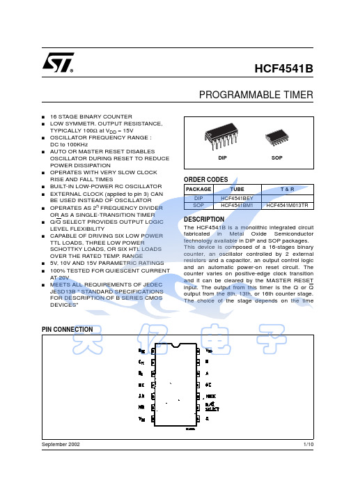
1/10September 2002s 16 STAGE BINARY COUNTERsLOW SYMMETR. OUTPUT RESISTANCE, TYPICALLY 100Ω at V DD = 15VsOSCILLATOR FREQUENCY RANGE :DC to 100KHzsAUTO OR MASTER RESET DISABLESOSCILLATOR DURING RESET TO REDUCE POWER DISSIPATIONsOPERATES WITH VERY SLOW CLOCK RISE AND FALL TIMESs BUILT-IN LOW-POWER RC OSCILLATOR sEXTERNAL CLOCK (applied to pin 3) CAN BE USED INSTEAD OF OSCILLATORsOPERATES AS 2n FREQUENCY DIVIDEROR AS A SINGLE-TRANSITION TIMER sQ/Q SELECT PROVIDES OUTPUT LOGIC LEVEL FLEXIBILITYsCAPABLE OF DRIVING SIX LOW POWER TTL LOADS, THREE LOW POWERSCHOTTKY LOADS, OR SIX HTL LOADS OVER THE RATED TEMP. RANGEs 5V, 10V AND 15V PARAMETRIC RATINGS s100% TESTED FOR QUIESCENT CURRENT AT 20VsMEETS ALL REQUIREMENTS OF JEDEC JESD13B " STANDARD SPECIFICATIONS FOR DESCRIPTION OF B SERIES CMOS DEVICES"DESCRIPTIONThe HCF4541B is a monolithic integrated circuit fabricated in Metal Oxide Semiconductor technology available in DIP and SOP packages. This device is composed of a 16-stages binary counter, an oscillator controlled by 2 external resistors and a capacitor, an output control logic and an automatic power-on reset circuit. The counter varies on positive-edge clock transition and it can be cleared by the MASTER RESET input. The output from this timer is the Q or Q output from the 8th, 13th, or 16th counter stage.The choice of the stage depends on the timeHCF4541BPROGRAMMABLE TIMERORDER CODESPACKAGE TUBE T & R DIP HCF4541BEY SOPHCF4541BM1HCF4541M013TRDIP SOPHCF4541B2/10select inputs A or B (see frequency selection table). The output is available in one of the two modes that can be selected via the MODE input pin 10 (see truth table). The output turns out as a continuos square wave, with a frequency equal to the oscillator frequency divided by 2N when this MODE input is a logic "1". When it is a logic "0"and after a MASTER RESET is started, and Q output has been selected, the output goes up to a high state after 2 N-1 counts. It remains in that state till another MASTER RESET pulse is apply or the mode input is a logic "1". The process starts by setting the AUTO RESET input (pin 5) to logic "0" and switching power on. If pin 5 is set to logic "1", the AUTO RESET circuit is not enabled and counting cannot start till a positive MASTER RESET pulse is applied, returning to a low level.The AUTO RESET consumes a remarkable amount of power and should not be used if low power operation is wanted. The frequency of the oscillator depends on the RC network. It can be calculated using the following formula : f = 1 / 2.3 R TC C TCwhere f is between 1KHz and 100KHz and RS >10 K Ω and ≈2 R TC INPUT EQUIVALENT CIRCUITPIN DESCRIPTIONRC OSCILLATOR CIRCUITPIN No SYMBOL NAME AND FUNCTION 12, 13A, B Time Select Input 4, 11NC Not Connected1, 2R TC , C TCExternal Resistor, Capaci-tor Connection3R S External Resistor Con-nection or External Clock Input5AR Auto Reset Input 6MR Master Reset Input 10MODE Mode Select Input 9Q/Q SELECTOutput Selector 8Q Output7V SS Negative Supply Voltage 14V DDPositive Supply VoltageHCF4541B3/10FUNCTIONAL DIAGRAMFREQUENCY SELECTION TABLETRUTH TABLELOGIC DIAGRAMA B N. of Stages NCount 2N L L 138192L H 101024H L 8256HH1665536PIN STATELH5Auto Reset On Auto Reset Disable 6Master Reset Off Master Reset On 9Output Initially Low After Reset (Q)Output Initially High After Reset (Q)10Single Transition ModeRecycle ModeHCF4541B4/10ABSOLUTE MAXIMUM RATINGSAbsolute Maximum Ratings are those values beyond which damage to the device may occur. Functional operation under these conditions is not implied.All voltage values are referred to V SS pin voltage.RECOMMENDED OPERATING CONDITIONSSymbol ParameterValue Unit V DD Supply Voltage -0.5 to +22V V I DC Input Voltage -0.5 to V DD + 0.5V I I DC Input Current± 10mA P D Power Dissipation per Package200mW Power Dissipation per Output Transistor 100mW T op Operating Temperature -55 to +125°C T stgStorage Temperature-65 to +150°CSymbol ParameterValue Unit V DD Supply Voltage 3 to 20V V I Input Voltage0 to V DD V T opOperating Temperature-55 to 125°CHCF4541B5/10DC SPECIFICATIONSThe Noise Margin for both "1" and "0" level is: 1V min. with V DD =5V, 2V min. with V DD =10V, 2.5V min. with V DD =15VSymbolParameterTest ConditionValue UnitV I (V)V O (V)|I O |(µA)V DD (V)T A = 25°C -40 to 85°C -55 to 125°C Min.Typ.Max.Min.Max.Min.Max.I LQuiescent Current0/550.045150150µA0/10100.0410*******/15150.04206006000/20200.0810030003000V OHHigh Level Output Voltage0/5<15 4.95 4.95 4.95V0/10<1109.959.959.950/15<11514.9514.9514.95V OLLow Level Output Voltage5/0<150.050.050.05V10/0<1100.050.050.0515/0<1150.050.050.05V IHHigh Level Input Voltage 0.5/4.5<15 3.5 3.5 3.5V1/9<1107771.5/13.5<115111111V ILLow Level Input Voltage 4.5/0.5<15 1.5 1.5 1.5V9/1<11033313.5/1.5<115444I OHOutput Drive Current0/5 2.5<15-1.55-3.1-1.08-1.08mA0/5 4.6<15-5-10-3-4.10/109.5<110-4-8-3.3-3.30/1513.5<115-10-20-8.4-8.4I OLOutput Sink Current0/50.4<15 1.55 3.1 1.08 1.08mA0/100.5<11048 3.3 3.30/15 1.5<11510208.48.4I IInput Leakage Current0/18Any Input 18±10-5±0.1±1±1µA C IInput CapacitanceAny Input57.5pFHCF4541B6/10DYNAMIC ELECTRICAL CHARACTERISTICS (T amb = 25°C, C L = 50pF, R L = 200K Ω, t r = t f = 20 ns)(*) Typical temperature coefficient for all V DD value is 0.3 %/°C.DIGITAL TIMER APPLICATIONA positive MASTER RESET pulse clears the counter and latch. The Output goes high and keeps up till the number of pulses, selected by A andB , are counted. This circuit is retriggerable and is as accurate as the input frequency. If a more accurate circuit is desired, an external clock can be used on pin 3. A set-up time equal to the width of the one shot output is required immediately following initial power up, during which time the output will be highSymbolParameterTest ConditionValue (*)UnitV DD (V)Min.Typ.Max.(28)t PHL t PLH Propagation Delay Time (CLOCK to Q)5 3.510.5µs 10 1.25 3.8150.9 2.9(216)t PHL t PLH Propagation Delay Time (CLOCK to Q)5618µs10 3.51015 2.57.5t THLTransition Time5100200ns1050100154080t TLHTransition Time5180360ns10901801565130Master Reset, Clock Pulse Width5900300ns103001001522585f CLMaximum Clock Pulse Input Frequency 5 1.5MHz104156t r, t fMaximum Clock Pulse Input Rise or Fall Time5Unlimitedµs1015HCF4541B7/10TEST CIRCUITL R L = 200K ΩR T = Z OUT of pulse generator (typically 50Ω)b0.50.020b10.250.010D200.787 E8.50.335e 2.540.100e315.240.600F7.10.280I 5.10.201L 3.30.130Z 1.27 2.540.0500.100P001A 8/10b0.350.460.0130.018b10.190.250.0070.010C0.50.019c145˚ (typ.)D8.558.750.3360.344E 5.8 6.20.2280.244e 1.270.050e37.620.300F 3.8 4.00.1490.157G 4.6 5.30.1810.208L0.5 1.270.0190.050M0.680.026S˚ (max.)8PO13G9/10HCF4541BInformation furnished is believed to be accurate and reliable. However, STMicroelectronics assumes no responsibility for the consequences of use of such information nor for any infringement of patents or other rights of third parties which may result from its use. No license is granted by implication or otherwise under any patent or patent rights of STMicroelectronics. Specifications mentioned in this publication are subject to change without notice. This publication supersedes and replaces all information previously supplied. STMicroelectronics products are not authorized for use as critical components in life support devices or systems without express written approval of STMicroelectronics.© The ST logo is a registered trademark of STMicroelectronics© 2002 STMicroelectronics - Printed in Italy - All Rights ReservedSTMicroelectronics GROUP OF COMPANIESAustralia - Brazil - Canada - China - Finland - France - Germany - Hong Kong - India - Israel - Italy - Japan - Malaysia - Malta - Morocco Singapore - Spain - Sweden - Switzerland - United Kingdom - United States.© 10/10。
任务书论文)课程设计(班 2014-1 专计算机科学与技术信息工程学院业简易家电定时控制装置题目一、课程设计(论文)29 日止。
月 2017 日起至年 6 19年)二、课程设计(论文工作自 2017 6月 : (三、课程设计论文) 地点 5#402内容要求:四、课程设计(论文)1.本课程设计的目的(1)使学生掌握系统各功能模块的基本工作原理;(2)培养学生基本掌握电路设计的基本思路和方法;)使学生掌握接收系统调试;(3 )培养学生分析、解决问题的能力;(4 (5)提高学生的科技论文写作能力。
.课程设计的任务及要求2 1)基本要求:(1)对家电的开启进行预定时控制,能显示并设置预定时间;(2)对家电的工作时间进行定时控制,能显示并通过键盘设置工作时间的长短;(3)工作时间到了后,并能声音报警;(4)设定时间时,黄色发光二极管点亮,启动定时后,红色发光二极管点亮。
2)创新要求:在基本要求达到后,可进行创新设计,如改善电路性能;对系统进行仿真分析。
)课程设计论文编写要求3要按照书稿的规格打印誊写毕业论文)1(论文包括目录、绪论、正文、小结、参考文献、谢辞、附录等)(2毕业论文装订按学校的统一要求完成(3) 4)答辩与评分标准:)完成原理分析:20分;(1 分;40(2)完成设计过程(含翻译):分;20(3)完成调试:分。
(4)回答问题:20)参考文献:5 人民邮电出版社仿真》和《单片机原理及应用技术——基于1()邓胡滨.Keil CProteus6)课程设计进度安排内容天数地点图书馆2构思及收集资料实验室5组装与调试图书馆、实验室3撰写论文学生签名:2017 年6 月19 日课程设计(论文)评审意见);)、中()、一般()、差((1)完成原理分析(20分):优()、良()、差)、一般()、良()、中((2)设计分析和翻译能力(40分):优((););)、一般()、差(20分):优()、良()、中()完成调试(3();)、差()、良()、中()、一般(20(4)回答问题(分):优())、否((5)格式规范性及考勤是否降等级:是(评阅人:职称:副教授日29 6 月2017 年目录绪论 (1)一、设计任务及要求 (2)1.1 设计目的 (2)1.2 基本功能要求 (2)1.3拓展功能设计 (2)1.4 功能详细设计 (3)二、硬件电路设计及描述 (3)2.1AT89C52单片机 (3)2.2 DS1302数码管显示时钟 (4)2.3矩阵按键电路 (5)2.4LCD液晶显示屏电路 (6)2.5LED数码管动态显示 (7)2.674HC138译码器 (9)2.7报警电路 (10)三、程序设计思想及流程 (11)四、电路的安装及调试 (12)4.1 安装步骤 (12)4.2 电路的调试 (12)五、总结 (12)六、参考文献 (13)七、附录 (13)7.1 实物图 (13)7.2仿真图 (13)7.3 部分程序清单 (14)绪论单片微计算机自20世纪70年代问世以来,已对人类社会产生了巨大的影响。

电子技术课程设计(报告)题目:数字钟设计与制作学院信息与电气工程学院专业电气工程及其自动化年级))0)姓名$学号2010*******指导教师******时间2012、12一:设计目的通过设计与实践,制作出具有准确显示时、分、秒的数字钟。
二:设计要求数字钟的功能要求:准确计时,以6位LED数码管形式显示时、分、秒的时间,小时计时要求为“24翻1”,分和秒的计时要求为60进制。
三:器件清单多功能数字钟主体电路元器件清单集成芯片:CD4543BP*6,CD4518BM*4,CD4060BM,74HC00D,CD4013BM,74HC14D电容:1000 uF,4700 uF,30pF,其他若干电阻:4.3Ω*42,4.7kΩ*4,470Ω,100Ω,1000kΩ主板,LED显示屏*6,开关*2,KB7206,L7805CV主要工具及附加材料:电烙铁、烙铁架、焊锡丝、松香、导线、镊子、钳子、数字万用表、吸锡器、剥线钳、等等。
四:电路原理(数字钟原理)数字钟的基本功能是显示时间,可以通过计数器的级联实现。
以4位数码管的数字钟为例,设定前两位为小时,后两位为分钟,数码管的小数点闪烁可以表示秒。
首先产生一个1Hz 的方波信号,在它的触发下驱动小数点闪烁。
在这个1Hz的基础上,可以产生1/60Hz的信号(对1Hz信号计数,每计数30次就将输出反相,得到1/60Hz信号),它就是分钟信号需要的时钟。
在这个时钟的触发下分钟位数码管依次加1,直到60时变为0,再重新开始计数。
清零的时候要产生一个进位,加到小时上面。
其他时间小时位保持不变五:各单元模块设计与分析1)晶体振荡器电路晶体振荡器电路给数字钟提供一个频率稳定准确的32.768KHZ的方波信号,可保证数字钟的走时准确及稳定。
本次设计采用了通过CMOS非门构成的电路。
如图(B)所示,由CMOS 非门U1与晶体、电容和电阻构成晶体振荡器电路,电容C1、C2与晶体构成一个谐振型网络,完成对振荡频率的控制功能,同时提供了一个180度相移,从而和非门构成一个正反馈网络,实现了振荡器的功能。
目录1前言 (1)2总体方案设计 (2)2.1设计内容 (2)2.2设计内容 (2)2.3方案论证 (3)2.4方案选择 (4)3单元模块设计 (5)3.1各单元模块功能介绍及电路设计 (5)3.1.1 温度采集电路 (5)3.1.2 DS1302时钟电路 (5)3.1.3 串行通信接口电路 (6)3.1.4 USB连接电路 (6)3.1.5 按键电路 (7)3.1.6液晶显示显示电路 (7)3.2特殊器件介绍 (7)3.2.1 STC89C52单片机芯片 (7)3.2.2 DS1302介绍 (8)3.2.3 温度传感器DS18B20 (9)3.2.4 液晶显示LCD1602 (9)4软件设计 (10)4.1软件选择 (10)4.2软件设计流程 (10)4.2.1 温度采集流程 (11)4.2.2 日期数据处理流程 (12)5系统的仿真及调试 (13)5.1系统仿真 (13)5.2硬件调试 (13)5.3软件调试 (14)6结论 (16)7总结与体会 (17)7.1设计小结 (17)7.2设计收获及改进 (17)7.3致谢 (17)8参考文献 (18)附录: (19)1前言单片机是指一个集成在一块芯片上的完整计算机系统。
尽管他的大部分功能集成在一块小芯片上,但是它具有一个完整计算机所需要的大部分部件:CPU、内存、内部和外部总线系统,目前大部分还会具有外存。
同时集成诸如通讯接口、定时器,实时时钟等外围设备。
而现在最强大的单片机系统甚至可以将声音、图像、网络、复杂的输入输出系统集成在一块芯片上。
单片机也被称为微控制器(Microcontroller),它不是完成某一个逻辑功能的芯片,而是把一个计算机系统集成到一个芯片上。
概括的讲:一块芯片就成了一台计算机。
它的体积小、质量轻、价格便宜、为学习、应用和开发提供了便利条件。
单片机诞生于20世纪70年代末,经历了SCM、MCU、SOC三大阶段。
STC单片机完全兼容51单片机,并有其独到之处,其抗干扰性强,加密性强,超低功耗,可以远程升级,内部有专用复位电路,价格也较便宜,由于这些特点使得 STC 系列单片机的应用日趋广泛。
基于单片机的定时器设计摘要:生活处处都有单片机,家里的所有电器只要是智能控制的都是单片机控制、现在智能手机中arm处理器也是一种高级单片机。
本文是对实时控制中的,实时显示这一功能进行进一步的研究。
实时控制系统,相对于其他的控制系统,最重要的一点就是实时。
文中的实时,指的是对时间的显示。
时间的显示包括对时、分的显示。
这些时间的显示,可以按照自己的需求进行进一步的设定。
这个实时系统,可以是通过串口接收的上位机,接收上位机中的信号,根据需求来进行时间的显示,帮助系统实现实时的效果。
同时,它可进行时间的独立显示。
利用STC89C51RC单片机作为本系统的中控模块。
上电后,按下功能键进入调时状态,通过各单元电路将按键部分设定的时间通过定时时间显示部分中的LED数码管显示出来。
中途可重新设置定时数值,复位部分除上电初实现复位外,也可人工复位。
关键词:实时;单片机;数码管;按键复位。
Based on single chip microcomputer timer designAbstract:Life is a single chip, all appliances at home as long as the intelligent control is now SCM control Intelligent mobile phone ARM processor is a kind of advanced single chip microcomputer.This article is in real-time control, real-time display this function for further studies. Real-time control system, relative to other control system, the most important thing is that in real time. In this paper, the real-time, refers to the display of time. The display includes pair, the display of the time. The display of the time, can according to your needs further. The real-time system, can be via a serial port to receive the upper machine, receiving signals in the PC, according to the demand for time display, help system to realize real time effect. At the same time, it can be independent of time.Using 89C51 microcontroller as the system control module. After power on, press the function key to transfer state, through each unit circuit timing LED digital display part of the display through the key part of the set time. You may re set the timer values, reset parts in addition to power up reset, the buttons can be reset at any time.Key Words : microcontrolle;digital tube;The Key to return.目录1引言 (1)1.1课题的来源和意义 (1)1.2定时器的应用 (1)1.3电子定时器的发展前景 (1)1.4 确定设计方案 (2)2 51单片机内部结构及计数原理 (2)2.1 51单片机内部机构 (2)2.2计数原理 (2)3 系统硬件配件设计 (4)3.1 芯片的选择 (4)3.2 交流控制接口电路 (5)3.3显示电路 (5)3.4 继电器 (5)3.5数码管 (6)4 硬件电路设计 (7)4.1 中继触发电路 (7)4.2继电器开关电路 (8)4.3时钟电路 (9)5 软件设计 (10)5.1 实现功能 (10)结论 (11)参考文献 (13)致谢 (14)附录1:程序 (15)附录2:系统仿真原理图 (21)1 引言我们在日常生活中,经常碰到一些需要定时的事情,例如:印相或放大照片,需要定在零点几秒的时间,洗衣机洗涤衣物需要定在几分钟到几十分钟的时间,电风扇需要定在数十分钟的时间。
电子技术课程设计题目24秒数显定时器专业测控技术与仪器指导教师宁志刚朱卫华班级测控技术与仪器071班2010年10月19日24秒数显定时器系统设计摘要:该系统选用三端集成稳压器7805所构成的直流稳压电源作为整个系统的供电部分,采用以石英晶体为核心的振荡电路为系统提供时钟脉冲,再通过4060和D触发器74LS74组成的分频电路对时钟脉冲进行15分频,最后产生1HZ脉冲。
利用两片74LS90组成的计数电路对1HZ脉冲进行24秒计数,再经过两片译码芯片CD4511进行译码,最后由共阴极七段数码管5161AS进行数显。
关键字:直流稳压电源,石英晶体,分频,译码,数显ABSTRACT:The system is an integrated selection of three-terminalregulator 7805 composed of DC power supply as the power supply part of the whole system, using quartz crystal oscillation circuit as the core of the system clock pulse, and through 4060, and the composition of D flip-flop 74LS74 divider circuit clock frequency for 15 minutes, finally resulting 1HZ pulse. Using two 74LS90 component count circuit 1HZ pulses 24 seconds count, and then after 2 decoding chip CD4511 decoding, and ultimately the common cathode seven-segment digital tube 5161AS to digital.KEYWORDS:DC Power,Crystal,Divider,Decoding,Digital display目录1系统方案设计 (4)1.1 设计任务与要求 (4)1.2 设计分析 (4)1.3各模块方案选择和论证 (4)1.3.1直流稳压电源模块的选择 (4)1.3.2 时钟脉冲产生模块的选择 (5)1.3.3分频电路模块的选择 (5)1.3.4计数电路模块的选择 (5)1.3.5译码数显电路模块的选择 (5)1.5 最终系统设计方案 (5)2各模块电路的设计及其原理图 (6)2.1直流稳压电源模块的设计 (6)2.2石英晶体振荡电路模块的设计 (7)2.3 分频电路模块的设计 (8)2.4 计数电路模块的设计 (10)2.5译码数显电路模块的设计 (11)3 收获体会 (14)参考文献 (15)附录: (16)附录一系统Protel原理图 (16)附录二系统Multisim仿真图 (17)附录三系统PCB图 (18)附录四元件清单 (19)1系统方案设计1.1 设计任务和要求:1.任务:根据数电模电知识,设计一个具有较高精度的24秒数显定时器。
毕业设计(论文)基于51单片机的智能定时控制器系统设计毕业设计(论文)任务书课题名称基于51单片机的智能定时控制器系统设计课题性质工程应用专业应用电子技术班级10电子(2)班学生姓名学号指导教师教研室主任系部主任发放日期一、课题条件:随着电子工业的发展,数字电子技术已经深入到了人们生活的各个层面,各种各样的电子产品也正在日新月异地向着高精尖技术发展。
数字电子时钟是一种用数字电路技术实现时、分、秒计时的装置,与机械式时钟相比具有更高的准确性和直观性,且无机械装置,具有更长的使用寿命,因此得到了广泛的使用。
二、毕业论文(设计)主要内容:1、时间显示:用4位数码管显示当前小时和分钟,秒功能用两LED灯代替(每秒闪烁一次)。
2、可手动设定时间。
3、开机流程:系统有红色和蓝色指示灯,上电10S内,每秒红色指示灯闪烁一次,并伴有蜂鸣声,作为开机/重启提醒,此时绿色指示灯灭。
10S后红色指示灯灭,若光线较强则绿色指示灯亮,若光线较弱则绿色指示灯亮度减半进入节能模式。
3、具有整点报时功能(四短一长),可自行设定报时时间段;三、计划进度:1. 资料的收集撰写开题报告6月20日至9月8日2. 方案设计9月9日至9月15日3. 电路的设计指标分析与确定;后期的电路优化元器件的选择与参数确定9月16日至11月2日4. 毕业设计论文的修改、完善11月3日至11月10日5. 毕业设计答辩11月15 日至11月20日四、主要参考文献:a)康光华主编.电子技术基础.北京:高等教育出版社,1999.6b)b)何宏主编.单片机原理与接口技术.北京:国防工业出版社.2006.07c)c)杨西明,朱骐主编.单片机编程与应用入门.北京:机械工业出版社.2004.06d)d)先锋工作室编著.单片机程序设计实例.北京:清华大学出版社.2003.01指导教师(系)教研室主任年月日年月日摘要本次设计以AT89C51芯片为核心,辅以必要的外围电路,设计了一个简易的电子时钟,它由5V直流电源供电。