MIKM9-7PL1中文资料
- 格式:pdf
- 大小:165.53 KB
- 文档页数:4


先锋M9基本信息本文章来源:主题名品网。
先锋M9是由中国北方先锋工业生产,在1998年开始为美国一家军品贸易公司生产D80刺刀,所有产品销往美国后由美国再销售到其它非美国国家。
刀身用不锈钢制造,经锻压加工,厚实坚固。
表面呈暗灰色。
刃口部位经局部热处理,刀口锋利,能砍树枝木棒,切割绳索。
发展历程1961年:美军开始装备M7式刺刀。
由于该刺刀只能作枪刺和匕首,功能较少,且刀颈部易锈蚀,被认为是世界上最差的刺刀之一,故在前苏联、英国等国军队采用多用途刺刀之后,美军提出了装备新刺刀的要求。
1985年12月:美陆军部正式提出对新刺刀的战术技术要求。
1986年初:五角大楼提出招标后,有3家美国公司和3家外国公司参加竞争。
经过对6家公司55把刺刀的野战试验,美国弗罗比斯公司的刺刀获胜中选,被命名为M9式多用刺刀。
此后在本宁堡美国步兵学校进行的步枪突击连刺刀突击科目训练中,又对M7式和M9式刺刀进行了广泛的对比试验。
试验结果,在损坏率等方面,M9式刺刀比M7式刺刀有明显的优越性。
1986年:美国陆军正式采用此型军用刺刀,并订其制式为M9系列多功能刺刀,简称M9MPBS。
1986年10月2日:由当时位于加州圣地牙哥郡Carsbad市的Phrobis Ltd·获得首批承包合约(合约批号:DAAA21-87-C0001)。
1986年10月:美国陆军部批准了一项价值1560万美元的合同,购买315600把M9式刺刀。
1987年2月:首批合约的部分刺刀开始交货,经由美国陆军验收后,拨交驻于本宁堡(Fort Bening)的美国陆军第75游骑兵营使用。
第一个主要配备部队则为美国陆军第七轻步兵师。
该型刺刀当时仅配发于美陆军步兵、游骑兵、特种部队及战斗工兵等部队。
1987年3月:M9式刺刀开始装备美陆军和少数特种部队。
1989年9月:Phrobis Ltd完成美陆军M9式刺刀第一个合约,产量为315,600把。
该批刺刀刀身标识为:M9 PHROBIS III U.S.A PAT PEND。

K7I 说明书K7I 是一款极高性价比,极其方便实用的ARM7-LPC2148学习板、开发板。
K7I 特别适用于ARM初学者。
K7I采用LPC2148主芯片。
片内资源::512K Flash+32K SRAM 。
用户可以自行焊接管脚pin对pin兼容的LPC214x芯片。
K7I可以通过USB(USB转串口技术)在线烧写(ISP)芯片内置FLASH,也可以通过JTAG烧写和在线调试。
K7I特点USB供电。
客户不需要配置额外的电源适配器。
USB烧写。
客户不需要配置额外的编程器。
USB接口。
适用于所有具有USB接口的电脑,客户不需要额外配置串口线或USB转串口电缆。
众多的资源。
接口全部开放。
先进的工艺。
双面板贴片设计。
提供全部设计资料。
包括原理图(orcad/pdf格式),原理图(PowerPCB格式)。
K7I 彩图K7I K7I标准套件标准套件标准套件K7I 主板 1块 165元(可单卖)USB 数据线 1根 2元(不单卖)Wiggler 兼容JTAG 板 1套 18元(不单卖)液晶 1602带背光 1片 15元(不单卖)K7I 价格价格K7I 主板(送USB 数据线) 165元K7I 标准套件 全国统一零售价198元三件以上团购三件以上团购,,送快递费送快递费!!K7I 快递服务快递服务K7I 一般采用顺丰快递,全国大部分地区38小时送货上门。
也可以由客户指定快递方式。
K7I K7I 购买办法购买办法购买办法1淘宝店 /店铺名字 K92 汇款工商银行卡号:9558 8040 0015 8957 742姓名:沈丽珍开户行:中国工商银行深圳高新产业园支行K7I 硬件资源LPC2148USB转串口LPC2148_USB 2.0 从接口1602液晶全modem接口SD卡数码管IIC EEPROMADDA4 KEY4 LED蜂鸣器温度传感器红外接收器(未焊)REALTIMEWatchDogJTAG全部引脚可供扩展使用K7I软件资源K7I提供测试用途的最终BIN码。

LM78M12中⽂资料LM341/LM78MXX Series3-Terminal Positive Voltage RegulatorsGeneral DescriptionThe LM341and LM78MXX series of three-terminal positive voltage regulators employ built-in current limiting,thermal shutdown,and safe-operating area protection which makes them virtually immune to damage from output overloads.With adequate heatsinking,they can deliver in excess of 0.5A output current.Typical applications would include local (on-card)regulators which can eliminate the noise and de-graded performance associated with single-point regulation.Featuresn Output current in excess of 0.5A n No external componentsn Internal thermal overload protection n Internal short circuit current-limitingn Output transistor safe-area compensationnAvailable in TO-220,TO-39,and TO-252D-PAK packagesn Output voltages of 5V,12V,and 15VConnection DiagramsTO-39Metal Can Package (H)DS010484-5Bottom ViewOrder Number LM78M05CH,LM78M12CH or LM78M15CHSee NS Package Number H03ATO-220Power Package (T)DS010484-6Top ViewOrder Number LM341T-5.0,LM341T-12,LM341T-15,LM78M05CT,LM78M12CT or LM78M15CTSee NS Package Number T03BTO-252DS010484-19Top ViewOrder Number LM78M05CDT See NS Package Number TD03BJuly 1999LM341/LM78MXX Series 3-Terminal Positive Voltage Regulators1999National Semiconductor Corporation /doc/96ef4d46852458fb770b5641.htmlAbsolute Maximum Ratings(Note1)If Military/Aerospace specified devices are required, please contact the National Semiconductor Sales Office/ Distributors for availability and specifications.Lead Temperature(Soldering,10seconds)TO-39Package(H)300?C TO-220Package(T)260?C Storage Temperature Range?65?C to+150?C Operating Junction TemperatureRange?40?C to+125?C Power Dissipation(Note2)Internally Limited Input Voltage5V≤V O≤15V35V ESD Susceptibility TBDElectrical CharacteristicsLimits in standard typeface are for T J=25?C,and limits in boldface type apply over the?40?C to+125?C operating temperature range.Limits are guaranteed by production testing or correlation techniques using standard Statistical Quality Control(SQC) methods.LM341-5.0,LM78M05CUnless otherwise specified:V IN=10V,C IN=0.33µF,C O=0.1µFSymbol Parameter Conditions Min Typ Max Units V O Output Voltage I L=500mA 4.8 5.0 5.2V5mA≤I L≤500mA 4.75 5.0 5.25P D≤7.5W,7.5V≤V IN≤20VV R LINE Line Regulation7.2V≤V IN≤25V I L=100mA50mVI L=500mA100V R LOAD Load Regulation5mA≤I L≤500mA100I Q Quiescent Current I L=500mA410.0mA ?I Q Quiescent Current Change5mA≤I L≤500mA0.57.5V≤V IN≤25V,I L=500mA 1.0V n Output Noise Voltage f=10Hz to100kHz40µVElectrical CharacteristicsLimits in standard typeface are for T J=25?C,and limits in boldface type apply over the?40?C to+125?C operating temperature range.Limits are guaranteed by production testing or correlation techniques using standard Statistical Quality Control(SQC) methods.(Continued)LM341-12,LM78M12CUnless otherwise specified:V IN=19V,C IN=0.33µF,C O=0.1µFSymbol Parameter Conditions Min Typ Max UnitsV O Output Voltage I L=500mA11.51212.5V5mA≤I L≤500mA11.41212.6P D≤7.5W,14.8V≤V IN≤27VV R LINE Line Regulation14.5V≤V IN≤30V I L=100mA120mVI L=500mA240V R LOAD Load Regulation5mA≤I L≤500mA240I Q Quiescent Current I L=500mA410.0mAI Q Quiescent Current Change5mA≤I L≤500mA0.514.8V≤V IN≤30V,I L=500mA 1.0V n Output Noise Voltage f=10Hz to100kHz75µVRipple Rejection f=120Hz,I L=500mA69dBV IN Input Voltage Required I L=500mA17.6V to Maintain Line RegulationV O Long Term Stability I L=500mA60mV/khrs Note1:Absolute maximum ratings indicate limits beyond which damage to the component may occur.Electrical specifications do not apply when operating the de-vice outside of its rated operating conditions.Note2:The typical thermal resistance of the three package types is:T(TO-220)package:θ(JA)=60?C/W,θ(JC)=5?C/WH(TO-39)package:θ(JA)=120?C/W,θ(JC)=18?C/WDT(TO-252)package:θ(JA)=92?C/W,θ(JC)=10?C/W3/doc/96ef4d46852458fb770b5641.htmlSchematic DiagramDS010484-1 /doc/96ef4d46852458fb770b5641.html 4 Typical Performance CharacteristicsPeak Output CurrentDS010484-10Ripple RejectionDS010484-11Ripple RejectionDS010484-12Dropout VoltageDS010484-13Output Voltage(Normalizedto1V at T J=25?C)DS010484-14Quiescent CurrentDS010484-15/doc/96ef4d46852458fb770b5641.html 5Typical Performance Characteristics(Continued)Design ConsiderationsThe LM78MXX/LM341XX fixed voltage regulator series has built-in thermal overload protection which prevents the de-vice from being damaged due to excessive junction tem-perature.The regulators also contain internal short-circuit protection which limits the maximum output current,and safe-area pro-tection for the pass transistor which reduces the short-circuit current as the voltage across the pass transistor is in-creased.Although the internal power dissipation is automatically lim-ited,the maximum junction temperature of the device must be kept below +125?C in order to meet data sheet specifica-tions.An adequate heatsink should be provided to assure this limit is not exceeded under worst-case operating condi-tions (maximum input voltage and load current)if reliable performance is to be obtained).1.0Heatsink ConsiderationsWhen an integrated circuit operates with appreciable cur-rent,its junction temperature is elevated.It is important to quantify its thermal limits in order to achieve acceptable per-formance and reliability.This limit is determined by summing the individual parts consisting of a series of temperature rises from the semiconductor junction to the operating envi-ronment.A one-dimension steady-state model of conduction heat transfer is demonstrated in The heat generated at thedevice junction flows through the die to the die attach pad,through the lead frame to the surrounding case material,to the printed circuit board,and eventually to the ambient envi-ronment.Below is a list of variables that may affect the ther-mal resistance and in turn the need for a heatsink.R θJC (Component Variables)R θCA (Application Variables)Leadframe Size &Material Mounting Pad Size,Material,&LocationNo.of Conduction Pins Placement of Mounting Pad Die SizePCB Size &Material Die Attach MaterialTraces Length &WidthMolding Compound Size and MaterialAdjacent Heat Sources Volume of Air Air FlowAmbient Temperature Shape of Mounting PadQuiescent CurrentDS010484-16Output ImpedanceDS010484-17Line Transient Response DS010484-7Load Transient ResponseDS010484-8/doc/96ef4d46852458fb770b5641.html6Design Considerations(Continued)The LM78MXX/LM341XX regulators have internal thermal shutdown to protect the device from over-heating.Under all possible operating conditions,the junction temperature of the LM78MXX/LM341XX must be within the range of 0?C to 125?C.A heatsink may be required depending on the maxi-mum power dissipation and maximum ambient temperature of the application.To determine if a heatsink is needed,the power dissipated by the regulator,P D ,must be calculated:I IN =I L +I GP D =(V IN ?V OUT )I L +V IN I Gshows the voltages and currents which are present in the circuit.The next parameter which must be calculated is the maxi-mum allowable temperature rise,T R (max):θJA =TR (max)/P D If the maximum allowable value for θJA ?C/w is found to be ≥60?C/W for TO-220package or ≥92?C/W for TO-252pack-age,no heatsink is needed since the package alone will dis-sipate enough heat to satisfy these requirements.If the cal-culated value for θJA fall below these limits,a heatsink is required.As a design aid,Table 1shows the value of the θJA of TO-252for different heatsink area.The copper patterns that we used to measure these θJA are shown at the end of the Application Note Section.reflects the same test results as what are in the Table 1shows the maximum allowable power dissipation vs.ambi-ent temperature for theTO-252device.shows the maximum allowable power dissipation vs.copper area (in 2)for the TO-252device.Please see AN1028for power enhancement techniques to be used with TO-252package.TABLE 1.θJA Different Heatsink AreaLayoutCopper AreaThermal Resistance Top Sice (in 2)*Bottom Side (in 2)(θJA ,?C/W)TO-25210.0123010320.06608730.306040.5305450.7605261047700.284800.470900.6631000.857110157120.0660.06689130.1750.17572140.2840.28461150.3920.39255160.50.553*Tab of device attached to topside copperDS010484-23FIGURE 1.Cross-sectional view of Integrated Circuit Mounted on a printed circuit board.Note that the case temperature is measured at the point where the leadscontact with the mounting pad surface DS010484-24FIGURE 2.Power Dissipation Diagram/doc/96ef4d46852458fb770b5641.html 7Design Considerations(Continued)Typical ApplicationDS010484-20FIGURE 3.θJA vs.2oz Copper Area for TO-252DS010484-22FIGURE 4.Maximum Allowable Power Dissipation vs.Ambient Temperature for TO-252DS010484-21FIGURE 5.Maximum Allowable Power Dissipation vs.2oz.Copper Area for TO-252DS010484-9*Required if regulator input is more than 4inches from input filter capacitor (or if no input filter capacitor is used).**Optional for improved transient response./doc/96ef4d46852458fb770b5641.html 8 Physical Dimensions inches(millimeters)unless otherwise notedTO-39Metal Can Package(H)Order Number LM78M05CH,LM78M12CH or LM78M15CHNS Package Number H03A9/doc/96ef4d46852458fb770b5641.htmlPhysical Dimensions inches(millimeters)unless otherwise noted(Continued)TO-220Power Package(T)Order Number LM341T-5.0,LM341T-12,LM341T-15,LM78M05CT,LM78M12CT or LM78M15CT NS Package Number T03B/doc/96ef4d46852458fb770b5641.html 10Physical Dimensionsinches (millimeters)unless otherwise noted (Continued)LIFE SUPPORT POLICYNATIONAL’S PRODUCTS ARE NOT AUTHORIZED FOR USE AS CRITICAL COMPONENTS IN LIFE SUPPORT DEVICES OR SYSTEMS WITHOUT THE EXPRESS WRITTEN APPROVAL OF THE PRESIDENT AND GENERAL COUNSEL OF NATIONAL SEMICONDUCTOR CORPORATION.As used herein:1.Life support devices or systems are devices or systems which,(a)are intended for surgical implant into the body,or (b)support or sustain life,and whose failure to perform when properly used in accordance with instructions for use provided in the labeling,can be reasonably expected to result in a significant injury to the user.2.A critical component is any component of a life support device or system whose failure to perform can be reasonably expected to cause the failure of the life support device or system,or to affect its safety or effectiveness.National Semiconductor Corporation AmericasTel:1-800-272-9959Fax:1-800-737-7018Email:support@/doc/96ef4d46852458fb770b5641.htmlNational Semiconductor EuropeFax:+49(0)180-5308586Email:europe.support@/doc/96ef4d46852458fb770b5641.htmlDeutsch Tel:+49(0)180-5308585English Tel:+49(0)180-5327832Fran?ais Tel:+49(0)180-5329358Italiano Tel:+49(0)180-5341680National Semiconductor Asia Pacific Customer Response Group Tel:65-2544466Fax:65-2504466Email:sea.support@/doc/96ef4d46852458fb770b5641.htmlNational Semiconductor Japan Ltd.Tel:81-3-5639-7560Fax:81-3-5639-7507/doc/96ef4d46852458fb770b5641.htmlTO-252Order Number LM78M05CDT NS Package Number TD03BLM341/LM78MXX Series 3-Terminal Positive Voltage RegulatorsNational does not assume any responsibility for use of any circuitry described,no circuit patent licenses are implied and National reserves the right at any time without notice to change said circuitry andspecifications.。

Features•Incorporates the ARM7TDMI ® ARM ® Thumb ® Processor–High-performance 32-bit RISC Architecture –High-density 16-bit Instruction Set – Leader in MIPS/Watt–EmbeddedICE ™ In-circuit Emulation, Debug Communication Channel Support •Internal High-speed Flash–512 Kbytes (AT91SAM7X512) Organized in Two Banks of 1024 Pages of 256 Bytes (Dual Plane)–256 Kbytes (AT91SAM7X256) Organized in 1024 Pages of 256 Bytes (Single Plane)–128 Kbytes (AT91SAM7X128) Organized in 512 Pages of 256 Bytes (Single Plane)– Single Cycle Access at Up to 30 MHz in Worst Case Conditions– Prefetch Buffer Optimizing Thumb Instruction Execution at Maximum Speed – Page Programming Time: 6 ms, Including Page Auto-erase,Full Erase Time: 15 ms– 10,000 Write Cycles, 10-year Data Retention Capability,Sector Lock Capabilities, Flash Security Bit– Fast Flash Programming Interface for High Volume Production •Internal High-speed SRAM, Single-cycle Access at Maximum Speed –128 Kbytes (AT91SAM7X512)–64 Kbytes (AT91SAM7X256)–32 Kbytes (AT91SAM7X128)•Memory Controller (MC)–Embedded Flash Controller, Abort Status and Misalignment Detection •Reset Controller (RSTC)–Based on Power-on Reset Cells and Low-power Factory-calibrated Brownout Detector–Provides External Reset Signal Shaping and Reset Source Status •Clock Generator (CKGR)–Low-power RC Oscillator, 3 to 20 MHz On-chip Oscillator and one PLL •Power Management Controller (PMC)–Power Optimization Capabilities, Including Slow Clock Mode (Down to 500 Hz) and Idle Mode–Four Programmable External Clock Signals •Advanced Interrupt Controller (AIC)–Individually Maskable, Eight-level Priority, Vectored Interrupt Sources–Two External Interrupt Sources and One Fast Interrupt Source, Spurious Interrupt Protected•Debug Unit (DBGU)–2-wire UART and Support for Debug Communication Channel interrupt, Programmable ICE Access Prevention •Periodic Interval Timer (PIT)–20-bit Programmable Counter plus 12-bit Interval Counter •Windowed Watchdog (WDT)–12-bit key-protected Programmable Counter–Provides Reset or Interrupt Signals to the System–Counter May Be Stopped While the Processor is in Debug State or in Idle Mode •Real-time Timer (RTT)–32-bit Free-running Counter with Alarm –Runs Off the Internal RC Oscillator26120DS–ATARM–03-Oct-06AT91SAM7X512/256/128 Preliminary Summary•Two Parallel Input/Output Controllers (PIO)–Sixty-two Programmable I/O Lines Multiplexed with up to Two Peripheral I/Os –Input Change Interrupt Capability on Each I/O Line–Individually Programmable Open-drain, Pull-up Resistor and Synchronous Output •Thirteen Peripheral DMA Controller (PDC) Channels•One USB 2.0 Full Speed (12 Mbits per second) Device Port–On-chip Transceiver, 1352-byte Configurable Integrated FIFOs •One Ethernet MAC 10/100 base-T–Media Independent Interface (MII) or Reduced Media Independent Interface (RMII)–Integrated 28-byte FIFOs and Dedicated DMA Channels for Transmit and Receive •One Part 2.0A and Part 2.0B Compliant CAN Controller–Eight Fully-programmable Message Object Mailboxes, 16-bit Time Stamp Counter •One Synchronous Serial Controller (SSC)–Independent Clock and Frame Sync Signals for Each Receiver and Transmitter –I²S Analog Interface Support, Time Division Multiplex Support–High-speed Continuous Data Stream Capabilities with 32-bit Data Transfer •Two Universal Synchronous/Asynchronous Receiver Transmitters (USART)–Individual Baud Rate Generator, IrDA ® Infrared Modulation/Demodulation–Support for ISO7816 T0/T1 Smart Card, Hardware Handshaking, RS485 Support –Full Modem Line Support on USART1•Two Master/Slave Serial Peripheral Interfaces (SPI)–8- to 16-bit Programmable Data Length, Four External Peripheral Chip Selects •One Three-channel 16-bit Timer/Counter (TC)–Three External Clock Inputs, Two Multi-purpose I/O Pins per Channel –Double PWM Generation, Capture/Waveform Mode, Up/Down Capability •One Four-channel 16-bit Power Width Modulation Controller (PWMC)•One Two-wire Interface (TWI)–Master Mode Support Only, All Two-wire Atmel EEPROMs Supported•One 8-channel 10-bit Analog-to-Digital Converter, Four Channels Multiplexed with Digital I/Os •SAM-BA ™ Boot Assistance –Default Boot program–Interface with SAM-BA Graphic User Interface •IEEE ® 1149.1 JTAG Boundary Scan on All Digital Pins•5V-tolerant I/Os, Including Four High-current Drive I/O lines, Up to 16 mA Each •Power Supplies–Embedded 1.8V Regulator, Drawing up to 100 mA for the Core and External Components –3.3V VDDIO I/O Lines Power Supply, Independent 3.3V VDDFLASH Flash Power Supply –1.8V VDDCORE Core Power Supply with Brownout Detector•Fully Static Operation: Up to 55 MHz at 1.65V and 85°C Worst Case Conditions •Available in 100-lead LQFP Green and 100-ball TFBGA Green Packages36120DS–ATARM–03-Oct-06AT91SAM7X512/256/128 Preliminary Summary1.DescriptionAtmel's AT91SAM7X512/256/128 is a member of a series of highly integrated Flash microcon-trollers based on the 32-bit ARM RISC processor. It features 512/256/128 Kbyte high-speed Flash and 128/64/32 Kbyte SRAM, a large set of peripherals, including an 802.3 Ethernet MAC and a CAN controller. A complete set of system functions minimizes the number of external components.The embedded Flash memory can be programmed in-system via the JTAG-ICE interface or via a parallel interface on a production programmer prior to mounting. Built-in lock bits and a secu-rity bit protect the firmware from accidental overwrite and preserve its confidentiality.The AT91SAM7X512/256/128 system controller includes a reset controller capable of managing the power-on sequence of the microcontroller and the complete system. Correct device opera-tion can be monitored by a built-in brownout detector and a watchdog running off an integrated RC oscillator.By combining the ARM7TDMI processor with on-chip Flash and SRAM, and a wide range of peripheral functions, including USART, SPI, CAN Controller, Ethernet MAC, Timer Counter, RTT and Analog-to-Digital Converters on a monolithic chip, the AT91SAM7X512/256/128 is a power-ful device that provides a flexible, cost-effective solution to many embedded control applications requiring communication over, for example, Ethernet, CAN wired and Zigbee ™ wireless networks.1.1Configuration Summary of the AT91SAM7X512/256/128The AT91SAM7X512, AT91SAM7X256 and AT91SAM7X128 differ only in memory sizes. Table 1-1 summarizes the configurations of the three devices.Table 1-1.Configuration SummaryDeviceFlash FlashOrganization SRAM A T91SAM7X512512 Kbytes dual plane 128 Kbytes A T91SAM7X256256 Kbytes single plane 64 Kbytes A T91SAM7X128128 Kbytessingle plane32 Kbytes46120DS–ATARM–03-Oct-06AT91SAM7X512/256/128 Preliminary Summary2.AT91SAM7X512/256/128 Block DiagramFigure 2-1.AT91SAM7X512/256/128 Block Diagram56120DS–ATARM–03-Oct-06AT91SAM7X512/256/128 Preliminary Summary3.Signal DescriptionTable 3-1.Signal Description ListSignal NameFunctionTypeActive LevelCommentsPowerVDDIN Voltage Regulator and ADC Power Supply InputPower 3V to 3.6V VDDOUT Voltage Regulator Output Power 1.85V VDDFLASH Flash and USB Power Supply Power 3V to 3.6V VDDIO I/O Lines Power Supply Power 3V to 3.6V VDDCORE Core Power Supply Power 1.65V to 1.95V VDDPLL PLL Power 1.65V to 1.95VGND GroundGroundClocks, Oscillators and PLLsXIN Main Oscillator Input Input XOUT Main Oscillator Output Output PLLRC PLL FilterInput PCK0 - PCK3Programmable Clock Output OutputICE and JTAGTCK Test Clock Input No pull-up resistor TDI Test Data In Input No pull-up resistor.TDO Test Data Out Output TMS Test Mode Select Input No pull-up resistor.JT AGSELJTAG SelectionInputPull-down resistor.Flash MemoryERASEFlash and NVM Configuration Bits Erase CommandInputHighPull-down resistor Reset/TestNRST Microcontroller Reset I/O Low Pull-up resistor, Open Drain OutputTST Test Mode SelectInput HighPull-down resistorDebug UnitDRXD Debug Receive Data Input DTXD Debug Transmit DataOutput AICIRQ0 - IRQ1External Interrupt Inputs Input FIQ Fast Interrupt InputInput PIOP A0 - P A30Parallel IO Controller A I/O Pulled-up input at reset PB0 - PB30Parallel IO Controller BI/OPulled-up input at reset66120DS–ATARM–03-Oct-06AT91SAM7X512/256/128 Preliminary SummaryUSB Device PortDDM USB Device Port Data - Analog DDP USB Device Port Data +AnalogUSARTSCK0 - SCK1Serial Clock I/O TXD0 - TXD1Transmit Data I/O RXD0 - RXD1 Receive Data Input RTS0 - RTS1Request T o Send Output CTS0 - CTS1Clear T o Send Input DCD1Data Carrier Detect Input DTR1Data Terminal Ready Output DSR1Data Set Ready Input RI1Ring Indicator InputSynchronous Serial ControllerTD Transmit Data Output RD Receive Data Input TK Transmit Clock I/O RK Receive Clock I/O TF Transmit Frame Sync I/O RFReceive Frame SyncI/O Timer/CounterTCLK0 - TCLK2External Clock Inputs Input TIOA0 - TIOA2I/O Line A I/O TIOB0 - TIOB2I/O Line B I/OPWM ControllerPWM0 - PWM3PWM Channels OutputSerial Peripheral Interface - SPIxSPIx_MISO Master In Slave Out I/O SPIx_MOSI Master Out Slave In I/O SPIx_SPCK SPI Serial ClockI/O SPIx_NPCS0SPI Peripheral Chip Select 0I/O Low SPIx_NPCS1-NPCS3SPI Peripheral Chip Select 1 to 3Output LowTwo-wire InterfaceTWD Two-wire Serial Data I/O TWCKTwo-wire Serial ClockI/OTable 3-1.Signal Description List (Continued)Signal Name FunctionTypeActive LevelComments76120DS–ATARM–03-Oct-06AT91SAM7X512/256/128 Preliminary SummaryAnalog-to-Digital ConverterAD0-AD3Analog Inputs Analog Digital pulled-up inputs at reset AD4-AD7Analog Inputs Analog Analog InputsADTRG ADC Trigger Input ADVREFADC Reference AnalogFast Flash Programming InterfacePGMEN0-PGMEN1Programming Enabling Input PGMM0-PGMM3Programming Mode Input PGMD0-PGMD15Programming Data I/O PGMRDY Programming Ready Output High PGMNVALID Data Direction Output Low PGMNOE Programming Read Input LowPGMCK Programming Clock Input PGMNCMD Programming Command InputLow CAN ControllerCANRX CAN Input Input CANTX CAN Output OutputEthernet MAC 10/100EREFCK Reference Clock Input RMII only ETXCK Transmit Clock Input MII only ERXCK Receive Clock Input MII onlyETXEN Transmit Enable Output ETX0 - ETX3Transmit Data Output ETX0 - ETX1 only in RMII ETXER Transmit Coding Error Output MII only ERXDV Receive Data ValidInput MII only ECRSDV Carrier Sense and Data Valid Input RMII onlyERX0 - ERX3Receive Data Input ERX0 - ERX1 only in RMII ERXER Receive Error Input ECRS Carrier Sense Input MII only ECOL Collision Detected Input MII onlyEMDC Management Data Clock Output EMDIO Management Data Input/Output I/O EF100Force 100 Mbits/sec.OutputHighRMII only Table 3-1.Signal Description List (Continued)Signal Name Function TypeActive LevelComments86120DS–ATARM–03-Oct-06AT91SAM7X512/256/128 Preliminary Summary4.PackageThe AT91SAM7X512/256/128 is available in 100-lead LQFP Green and 100-ball TFBGA RoHS-compliant packages.4.1100-lead LQFP Package OutlineFigure 4-1 shows the orientation of the 100-lead LQFP package. A detailed mechanical descrip-tion is given in the Mechanical Characteristics section.Figure 4-1.100-lead LQFP Package Outline (Top View)96120DS–ATARM–03-Oct-06AT91SAM7X512/256/128 Preliminary Summary4.2100-lead LQFP PinoutTable 4-1.Pinout in 100-lead LQFP Package1ADVREF 26P A18/PGMD651TDI 76TDO 2GND 27PB952GND 77JTAGSEL 3AD428PB853PB1678TMS 4AD529PB1454PB479TCK 5AD630PB1355P A23/PGMD1180P A306AD731PB656P A24/PGMD1281P A0/PGMEN07VDDOUT 32GND 57NRST 82P A1/PGMEN18VDDIN 33VDDIO 58TST83GND 9PB27/AD034PB559P A25/PGMD1384VDDIO 10PB28/AD135PB1560P A26/PGMD1485P A311PB29/AD236PB1761VDDIO 86P A212PB30/AD337VDDCORE62VDDCORE 87VDDCORE 13P A8/PGMM038PB763PB1888P A4/PGMNCMD 14P A9/PGMM139PB1264PB1989P A5/PGMRDY 15VDDCORE 40PB065PB2090P A6/PGMNOE 16GND 41PB166PB2191P A7/PGMNVALID17VDDIO 42PB267PB2292ERASE 18P A10/PGMM243PB368GND 93DDM 19P A11/PGMM344PB1069PB2394DDP 20P A12/PGMD045PB1170PB2495VDDFLASH21P A13/PGMD146P A19/PGMD771PB2596GND 22P A14/PGMD247P A20/PGMD872PB2697XIN/PGMCK 23P A15/PGMD348VDDIO 73P A27/PGMD1598XOUT 24P A16/PGMD449P A21/PGMD974P A2899PLLRC 25P A17/PGMD550P A22/PGMD1075P A29100VDDPLL106120DS–ATARM–03-Oct-06AT91SAM7X512/256/128 Preliminary Summary4.3100-ball TFBGA Package OutlineFigure 4-2 shows the orientation of the 100-ball TFBGA package. A detailed mechanical description is given in the Mechanical Characteristics section of the full datasheet.Figure 4-2.100-ball TFBGA Package Outline (Top View)4.4100-ball TFBGA PinoutPinout in 100-ball TFBGA PackagePinSignal NamePinSignal NamePinSignal NamePinSignal NameA1P A22/PGMD10C6PB17F1PB21H6P A7/PGMNVALID A2P A21/PGMD9C7PB13F2PB23H7P A9/PGMM1A3P A20/PGMD8C8P A13/PGMD1F3PB25H8P A8/PGMM0A4PB1C9P A12/PGMD0F4PB26H9PB29/AD2A5PB7C10P A15/PGMD3F5TCKH10PLLRC A6PB5D1P A23/PGMD11F6P A6/PGMNOEJ1P A29A7PB8D2P A24/PGMD12F7ERASE J2P A30A8PB9D3NRST F8VDDCORE J3P A0/PGMEN0A9P A18/PGMD6D4TST F9GND J4P A1/PGMEN1A10VDDIO D5PB19F10VDDIN J5VDDFLASHB1TDID6PB6G1PB22J6GND B2P A19/PGMD7D7P A10/PGMM2G2PB24J7XIN/PGMCK B3PB11D8VDDIO G3P A27/PGMD15J8XOUT B4PB2D9PB27/AD0G4TDO J9GND B5PB12D10P A11/PGMM3G5P A2J10VDDPLL B6PB15E1P A25/PGMD13G6P A5/PGMRDY K1VDDCORE B7PB14E2P A26/PGMD14G7VDDCORE K2VDDCORE B8P A14/PGMD2E3PB18G8GND K3DDP B9P A16/PGMD4E4PB20G9PB30/AD3K4DDM B10P A17/PGMD5E5TMS G10VDDOUT K5GND C1PB16E6GND H1VDDCORE K6AD7C2PB4E7VDDIO H2P A28K7AD6C3PB10E8PB28/AD1H3JTAGSEL K8AD5C4PB3E9VDDIO H4P A3K9AD4C5PB0E10GNDH5P A4/PGMNCMDK10ADVREF116120DS–ATARM–03-Oct-06AT91SAM7X512/256/128 Preliminary Summary5.Power Considerations5.1Power SuppliesThe AT91SAM7X512/256/128 has six types of power supply pins and integrates a voltage regu-lator, allowing the device to be supplied with only one voltage. The six power supply pin types are:•VDDIN pin. It powers the voltage regulator and the ADC; voltage ranges from 3.0V to 3.6V , 3.3V nominal. In order to decrease current consumption, if the voltage regulator and the ADC are not used, VDDIN, ADVREF , AD4, AD5, AD6 and AD7 should be connected to GND. In this case, VDDOUT should be left unconnected.•VDDOUT pin. It is the output of the 1.8V voltage regulator.•VDDIO pin. It powers the I/O lines; voltage ranges from 3.0V to 3.6V, 3.3V nominal.•VDDFLASH pin. It powers the USB transceivers and a part of the Flash and is required for the Flash to operate correctly; voltage ranges from 3.0V to 3.6V , 3.3V nominal.•VDDCORE pins. They power the logic of the device; voltage ranges from 1.65V to 1.95V, 1.8V typical. It can be connected to the VDDOUT pin with decoupling capacitor. VDDCORE is required for the device, including its embedded Flash, to operate correctly.•VDDPLL pin. It powers the oscillator and the PLL. It can be connected directly to the VDDOUT pin.No separate ground pins are provided for the different power supplies. Only GND pins are pro-vided and should be connected as shortly as possible to the system ground plane.5.2Power ConsumptionThe AT91SAM7X512/256/128 has a static current of less than 60 µA on VDDCORE at 25°C,including the RC oscillator, the voltage regulator and the power-on reset when the brownout detector is deactivated. Activating the brownout detector adds 28 µA static current.The dynamic power consumption on VDDCORE is less than 90 mA at full speed when running out of the Flash. Under the same conditions, the power consumption on VDDFLASH does not exceed 10 mA.5.3Voltage RegulatorThe AT91SAM7X512/256/128 embeds a voltage regulator that is managed by the System Controller.In Normal Mode, the voltage regulator consumes less than 100 µA static current and draws 100mA of output current.The voltage regulator also has a Low-power Mode. In this mode, it consumes less than 25 µA static current and draws 1 mA of output current.Adequate output supply decoupling is mandatory for VDDOUT to reduce ripple and avoid oscil-lations. The best way to achieve this is to use two capacitors in parallel: one external 470 pF (or 1 nF) NPO capacitor should be connected between VDDOUT and GND as close to the chip as possible. One external 2.2 µF (or 3.3 µF) X7R capacitor should be connected between VDDOUT and GND.126120DS–ATARM–03-Oct-06AT91SAM7X512/256/128 Preliminary SummaryAdequate input supply decoupling is mandatory for VDDIN in order to improve startup stability and reduce source voltage drop. The input decoupling capacitor should be placed close to the chip. For example, two capacitors can be used in parallel: 100 nF NPO and 4.7 µF X7R.5.4Typical Powering SchematicsThe AT91SAM7X512/256/128 supports a 3.3V single supply mode. The internal regulator input connected to the 3.3V source and its output feeds VDDCORE and the VDDPLL. Figure 5-1shows the power schematics to be used for USB bus-powered systems.Figure 5-1.3.3V System Single Power Supply Schematic136120DS–ATARM–03-Oct-06AT91SAM7X512/256/128 Preliminary Summary6.I/O Lines Considerations6.1JTAG Port PinsTMS, TDI and TCK are schmitt trigger inputs and are not 5-V tolerant. TMS, TDI and TCK do not integrate a pull-up resistor.TDO is an output, driven at up to VDDIO, and has no pull-up resistor.The JTAGSEL pin is used to select the JTAG boundary scan when asserted at a high level. The JTAGSEL pin integrates a permanent pull-down resistor of about 15 k Ω to GND, so that it can be left unconnected for normal operations.6.2Test PinThe TST pin is used for manufacturing test or fast programming mode of the AT91SAM7X512/256/128 when asserted high. The TST pin integrates a permanent pull-down resistor of about 15 k Ω to GND, so that it can be left unconnected for normal operations. To enter fast programming mode, the TST pin and the PA0 and PA1 pins should be tied high and PA2 tied to low.Driving the TST pin at a high level while PA0 or PA1 is driven at 0 leads to unpredictable results.6.3Reset PinThe NRST pin is bidirectional with an open drain output buffer. It is handled by the on-chip reset controller and can be driven low to provide a reset signal to the external components or asserted low externally to reset the microcontroller. There is no constraint on the length of the reset pulse,and the reset controller can guarantee a minimum pulse length. This allows connection of a sim-ple push-button on the NRST pin as system user reset, and the use of the signal NRST to reset all the components of the system.The NRST pin integrates a permanent pull-up resistor to VDDIO .6.4ERASE PinThe ERASE pin is used to re-initialize the Flash content and some of its NVM bits. It integrates a permanent pull-down resistor of about 15 k Ω to GND, so that it can be left unconnected for nor-mal operations.This pin is debounced by the RC oscillator to improve the glitch tolerance. When the pin is tied to high during less than 100 ms, ERASE pin is not taken into account. The pin must be tied high during more than 220 ms to perform the re-initialization of the Flash.6.5PIO Controller LinesAll the I/O lines, PA0 to PA30 and PB0 to PB30, are 5V-tolerant and all integrate a programma-ble pull-up resistor. Programming of this pull-up resistor is performed independently for each I/O line through the PIO controllers.5V-tolerant means that the I/O lines can drive voltage level according to VDDIO, but can be driven with a voltage of up to 5.5V. However, driving an I/O line with a voltage over VDDIO while the programmable pull-up resistor is enabled will create a current path through the pull-up resis-146120DS–ATARM–03-Oct-06AT91SAM7X512/256/128 Preliminary Summarytor from the I/O line to VDDIO. Care should be taken, in particular at reset, as all the I/O lines default to input with pull-up resistor enabled at reset.6.6I/O Lines Current DrawingThe PIO lines PA0 to PA3 are high-drive current capable. Each of these I/O lines can drive up to 16 mA permanently.The remaining I/O lines can draw only 8 mA.However, the total current drawn by all the I/O lines cannot exceed 200 mA.156120DS–ATARM–03-Oct-06AT91SAM7X512/256/128 Preliminary Summary7.Processor and Architecture7.1ARM7TDMI Processor•RISC processor based on ARMv4T Von Neumann architecture–Runs at up to 55 MHz, providing 0.9 MIPS/MHz •Two instruction sets–ARM high-performance 32-bit instruction set –Thumb high code density 16-bit instruction set •Three-stage pipeline architecture–Instruction Fetch (F)–Instruction Decode (D)–Execute (E)7.2Debug and Test Features•Integrated embedded in-circuit emulator–Two watchpoint units–Test access port accessible through a JTAG protocol –Debug communication channel •Debug Unit–Two-pinUART–Debug communication channel interrupt handling –Chip ID Register•IEEE1149.1 JT AG Boundary-scan on all digital pins7.3Memory Controller•Programmable Bus Arbiter–Handles requests from the ARM7TDMI, the Ethernet MAC and the Peripheral DMA Controller•Address decoder provides selection signals for–Three internal 1 Mbyte memory areas –One 256 Mbyte embedded peripheral area •Abort Status Registers–Source, Type and all parameters of the access leading to an abort are saved –Facilitates debug by detection of bad pointers •Misalignment Detector–Alignment checking of all data accesses –Abort generation in case of misalignment •Remap Command–Remaps the SRAM in place of the embedded non-volatile memory –Allows handling of dynamic exception vectors166120DS–ATARM–03-Oct-06AT91SAM7X512/256/128 Preliminary Summary•Embedded Flash Controller–Embedded Flash interface, up to three programmable wait states–Prefetch buffer, buffering and anticipating the 16-bit requests, reducing the required wait states–Key-protected program, erase and lock/unlock sequencer –Single command for erasing, programming and locking operations –Interrupt generation in case of forbidden operation7.4Peripheral DMA Controller•Handles data transfer between peripherals and memories •Thirteen channels–Two for each USART –Two for the Debug Unit–Two for the Serial Synchronous Controller –Two for each Serial Peripheral Interface –One for the Analog-to-digital Converter •Low bus arbitration overhead–One Master Clock cycle needed for a transfer from memory to peripheral –Two Master Clock cycles needed for a transfer from peripheral to memory •Next Pointer management for reducing interrupt latency requirements176120DS–ATARM–03-Oct-06AT91SAM7X512/256/128 Preliminary Summary8.Memories8.1AT91SAM7X512•512 Kbytes of dual-plane Flash Memory–2 contiguous banks of 1024 pages of 256 bytes–Fast access time, 30 MHz single-cycle access in Worst Case conditions –Page programming time: 6 ms, including page auto-erase –Page programming without auto-erase: 3 ms –Full chip erase time: 15 ms–10,000 write cycles, 10-year data retention capability –32 lock bits, protecting 32 sectors of 64 pages –Protection Mode to secure contents of the Flash •128 Kbytes of Fast SRAM–Single-cycle access at full speed8.2AT91SAM7X256•256 Kbytes of Flash Memory–1024 pages of 256 bytes–Fast access time, 30 MHz single-cycle access in Worst Case conditions –Page programming time: 6 ms, including page auto-erase –Page programming without auto-erase: 3 ms –Full chip erase time: 15 ms–10,000 write cycles, 10-year data retention capability –16 lock bits, each protecting 16 sectors of 64 pages –Protection Mode to secure contents of the Flash •64 Kbytes of Fast SRAM–Single-cycle access at full speed8.3AT91SAM7X128•128 Kbytes of Flash Memory–512 pages of 256 bytes–Fast access time, 30 MHz single-cycle access in Worst Case conditions –Page programming time: 6 ms, including page auto-erase –Page programming without auto-erase: 3 ms –Full chip erase time: 15 ms–10,000 write cycles, 10-year data retention capability –8 lock bits, each protecting 8 sectors of 64 pages –Protection Mode to secure contents of the Flash •32 Kbytes of Fast SRAM–Single-cycle access at full speed186120DS–ATARM–03-Oct-06AT91SAM7X512/256/128 Preliminary SummaryFigure 8-1.AT91SAM7X512/256/128 Memory Mapping196120DS–ATARM–03-Oct-06AT91SAM7X512/256/128 Preliminary Summary8.4Memory Mapping8.4.1Internal SRAM•The AT91SAM7X512 embeds a high-speed 128 Kbyte SRAM bank.•The AT91SAM7X256 embeds a high-speed 64 Kbyte SRAM bank.•The AT91SAM7X128 embeds a high-speed 32 Kbyte SRAM bank.After reset and until the Remap Command is performed, the SRAM is only accessible at address 0x0020 0000. After Remap, the SRAM also becomes available at address 0x0.8.4.2Internal ROMThe AT91SAM7X512/256/128 embeds an Internal ROM. At any time, the ROM is mapped at address 0x30 0000. The ROM contains the FFPI and the SAM-BA program.8.4.3Internal Flash•The AT91SAM7X512 features two banks (dual plane) of 256 Kbytes of Flash.•The AT91SAM7X256 features one bank (single plane) of 256 Kbytes of Flash. •The AT91SAM7X128 features one bank (single plane) of 128 Kbytes of Flash.At any time, the Flash is mapped to address 0x0010 0000. It is also accessible at address 0x0after the reset, if GPNVM bit 2 is cleared and before the Remap Command.A general purpose NVM (GPNVM) bit is used to boot either on the ROM (default) or from the Flash.This GPNVM bit can be cleared or set respectively through the commands “Clear General-pur-pose NVM Bit” and “Set General-purpose NVM Bit” of the EFC User Interface.Setting the GPNVM Bit 2 selects the boot from the Flash. Asserting ERASE clears the GPNVM Bit 2 and thus selects the boot from the ROM by default.Figure 8-2.Internal Memory Mapping with GPNVM Bit 2 = 0 (default)206120DS–ATARM–03-Oct-06AT91SAM7X512/256/128 Preliminary SummaryFigure 8-3.Internal Memory Mapping with GPNVM Bit 2 = 18.5Embedded Flash8.5.1Flash Overview•The Flash of the AT91SAM7X512 is organized in two banks (dual plane) of 1024 pages of 256 bytes. The 524,288 bytes are organized in 32-bit words.•The Flash of the AT91SAM7X256 is organized in 1024 pages of 256 bytes (single plane). It reads as 65,536 32-bit words.•The Flash of the AT91SAM7X128 is organized in 512 pages of 256 bytes (single plane). It reads as 32,768 32-bit words.The Flash contains a 256-byte write buffer, accessible through a 32-bit interface.The Flash benefits from the integration of a power reset cell and from the brownout detector.This prevents code corruption during power supply changes, even in the worst conditions.When Flash is not used (read or write access), it is automatically placed into standby mode.8.5.2Embedded Flash ControllerThe Embedded Flash Controller (EFC) manages accesses performed by the masters of the sys-tem. It enables reading the Flash and writing the write buffer. It also contains a User Interface,mapped within the Memory Controller on the APB. The User Interface allows:•programming of the access parameters of the Flash (number of wait states, timings, etc.)•starting commands such as full erase, page erase, page program, NVM bit set, NVM bit clear, etc.•getting the end status of the last command •getting error status•programming interrupts on the end of the last commands or on errorsThe Embedded Flash Controller also provides a dual 32-bit Prefetch Buffer that optimizes 16-bit access to the Flash. This is particularly efficient when the processor is running in Thumb mode.Two EFCs are embedded in the AT91SAM7X512 to control each bank of 256 KBytes. Dual-plane organization allows concurrent read and program functionality. Read from one memory。

MICRO-K microminiature circular connectors are rugged yet lightweight - and meet or exceed the applicable requirements of MIL-DTL-83513. Applications include biomedical,instrumentation and miniature black boxes.MIK:Accommodate up to 55 contacts on .050(1.27) centers (equivalent to 420 contacts per square inch). Five keyway polarization prevents cross plugging. The threaded coupling nuts provide strong, reliable coupling. MIK recepta-cles can be either front or back panel mounted;in back mounting applications, panel thickness of up to 3/32" can be used on the larger sizes.Maximum temperature range - 55˚C to + 125˚C.Standard MIK connectors are available in two shell sizes accommodating two contact arrangements pre-wired to your specific requirements.MIKM:Similar to our MIK, except has a steel shell and receptacle for improved ruggedness and RFI resistance. It accommodates up to 85twist pin contacts. Maximum temperature range - 55˚C to + 125˚ C.MIKQ:A quick disconnect metal shell and receptacle version that can be instantaneously disconnected yet provides a solid lock when engaged. Applications include commercial TV cameras, portableradios, military gun sights, airborne landing systems and medical equipment. Maximum temperature range - 55˚C to +125˚C.SpecificationsSTANDARD MATERIAL AND FINISHESELECTRO/MECHANICAL FEATURES*For plug onlyElectrodeposited for receptacle.MIKThermoplastic Stainless Steel Passivated Glass-reinforced Thermoplastic 50Microinch Gold Plated Copper AlloyStainless Steel Stainless Steel Passivated Glass-reinforced Thermoplastic 50Microinch Gold Plated Copper AlloyBrass Brass, Electroless Nickel Plated*Glass-reinforced Thermoplastic 50Microinch Gold Plated Copper AlloyNo. of Contacts Wire SizeContact Termination Contact Rating Couping Polarization Contact Spacing Shell Styles 7,55#24 AWG thru #32 AWGCrimp 3Amps Threaded Keyways .050 (1.27)Centers0-Wall Mtg.6-Straight Plug7,55, 85#24 AWG thru #32 AWGCrimp 3Amps Threaded Keyways .050 (1.27)Centers 0-Wall Mtg.6-Straight Plug7,19, 37#24 AWG thru #32 AWGCrimp 3Amps Push/Pull Keyways .050 (1.27)Centers 7-Jam Nut 6-Straight Plug 9-Rear Panel Mtg. ReceptacleShellCoupling Nut Insulator ContactsMIKM MIKQ MIKMIKMMIKQ How to OrderSERIESMIK M 6-55P** ** * *SERIESMIK: Microminiature Circular7, 19, 37, 55, 85(H) 001 -18", 7/34 strand, #26 AWG,MIL-W-16878/4, Type E Teflon,yellow.18",7/34 strand, #26 AWG,MIL-W-16878/4, Type E Teflon,color coded to MIL-STD-681System I.1/2" uninsulated solid #25AWG gold plated copper.1" uninsulated solid #25 AWG gold plated copper.(H) 003 -(L)1-(L)2-G -Cable nut and grip (MIKQ plug only)N -Nut only (MIKQ plug only)NOTE: Contact types cannot be interchanged between shell styles.P -Pin S -SocketH -Insulated round hook-up wire L -Uninsulated round solid wireNo Letter - Screw couping, plastic shell M -Screw coupling, metal shell Q -Push/Pull, metal shell 0-Wall mounting receptacle (MIK and MIKM only)6-Straight plug (MIK, MIKM and MIKQ)7-Jam nut mount (MIKQ only)9-Rear panel mounted receptacle (MIKQ)CONNECTOR TYPESSHELL STYLESCONNECTOR TYPE SHELL STYLECONTACT ARRANGEMENT CONTACT ARRANGEMENTS CONTACT TYPE CONTACT TYPE TERMINATION TYPETERMINATION TYPESTERMINATION LENGTH CODE TERMINATION LENGTH CODE (STANDARDS)HARDWAREHARDWARERoHS COMPLIANCE RStandard Wire Termination CodesThe following termination codes are listed for your information. For additional codes please refer to Appendix on page 79 and 81. All wire lengths are minimum.HARNESS TYPES (H)#26 A WG per MIL-W-16878Type E,Teflon S tranded L ength020019026029028001038009010011013017042027016034025002003023004005006048046041 3(76.2)6(152.4)8(203.2)10(254.0)12(304.8)18(457.2)20(508.0)24(609.6)30(762.0)36(914.4)48(1219.2)72(1828.8)120(3048.0)-All Yell o w Co l o r Cod e dContact ArrangementsFace View, Pin Side-(Male Twist Pin Contacts)MIK/MIKM/MIKQ7Contacts394857473831535512MIKQ19 ContactsMIKQ37 ContactsMIK/MIKM55 ContactsMIKM85 ContactsCavity identification numbers are for reference only, they do not appear on connectors.Shell Dimensions.335 (8.51)Max.MIK (Rear Panel Mount Thickness - see Tabulation "T")Weight given is 1/2" uninsulated, solid #25 AWG gold plated copper pigtailsPlu g Rece p tacleS hell S i z e7onl yRece p tacleS hell S i z e55 onl yPlu gPlugPart Numberby Shell SizeMIK6-7PMIK6-55PAThreadDMax.LMax.Avg. Weightoz. (gm.) ±5%5/16-24UNF-2B9/16-24UNF-2A.375 (9.52).755 (19.18).315 (8.00).460 (11.68).054 (1.54).202 (5.72)Part Numberby Shell SizeMIK0-7SMIK0-55SAThreadD±.010 (0.25)FMax.H±.003 (0.08)K±.010 (0.25)LMax.R±.005 (0.13)SMax.TMax.Avg. Weightoz. (gm.) ± 5% 5/16-24UNF-2B9/16-24UNF-2A.325 (8.26).625 (15.88).315 (8.00).440 (11.18).078 (1.98).089 (2.26).062 (1.57).100 (2.54).355 (9.02).495 (12.57).460 (11.68).580 (14.73).630 (16.00).760 (19.30).032 (0.81).062 (1.57).022 (.635).134 (3.81) ReceptacleShell Dimensions (Continued)MIKM (Rear Panel Mount Thickness .335 (8.51) max. - see Tabulation "T")D ..335 (8M a D.PlugReceptacleShell Size 7 onlyReceptacle Receptacle Shell Size 55 & 85PlugPlugMIKM6-7P 5/16-24UNF-2A.375(9.52) .315 (8.00) .054 (1.54)MIKM6-55P 5/8-24UNEF-2B.775(19.18) .440 (11.18) .333 (9.44) MIKM6-85P 11/16-24UNEF-2B .860 (21.84).460 (11.68).419 (11.88)MIKM0-7S 5/16-24UNF-2A .325 (8.26).320 (8.13) .078 (1.98) .062 (1.57) .400 (10.16) .460 (11.68).630 (16.00) .032 (0.81) .051 (1.45) MIKM0-55S 5/8-24UNEF-2A .625 (15.88).440 (11.18) .091 (2.31) .062 (1.57) .490 (12.45) .580 (14.73) .760 (19.30) .125 (3.18) .269 (7.62)MIKM0-85S 11/16-24UNEF-2A .745 (18.92) .440 (11.18).091 (2.31).062 (1.57).490 (12.45) .674 (17.12) .845 (21.46) .125 (3.18) .346 (9.80)Part Numberby Shell SizePart Number by Shell SizeA ThreadD Max.L Max.Avg. Weightoz. (gm.)+_5%A ThreadDF Max.H +_.003 (0.08)K L Max.R +_.005 (0.13)SMax.T Max.Avg. Weight oz. (gm.)+_5%MIKQ6-7S .385(9.78) .305 (7.75) .180 (4.57) .214 (6.08)MIKQ6-19S .515(13.08) .405 (10.29) .260 (6.60) .376 (10.70)MIKQ6-37S.760 (19.30).635 (16.13).350 (8.89).714 (20.23)MIKQ6-7S .510(12.95) .245 (6.22) .359 (9.12) 3/8-32UNEF-2A .128 (3.63)MIKQ7-37P.855(21.71).520 (13.20).740 (18.80)3/4-20UNEF-2A.300 (8.52)MIKQ (Front Panel Mounting Type Shown-.093 (2.36) Thickness)C .043±.005 C DIM.ACROSS FLA TPlugPlugReceptacle Receptacle*Std. Conn. not supplied with Cable Nut & Grip, See Mod Codes. Lanyard Relase Is Available. Consult factory.Part Number by Shell Size A MAX.B MAX.C Ref.Avg. Weight oz. (gm.)±5%Part Number by Shell Size A MAX.B MAX.C MAX.D Thread Avg. Weightoz. (gm.)±5%Front Panel Mounting-MIKQ7MIKQ Front Panel MountingMIKQ7-7P .364(9.24) .390 (9.91)MIKQ7-19P .475(12.06) .515 (13.08)MIKQ7-37P .740(18.78) .755 (19.17)Shell SizeA ±.005 (0.13)BDIA.Shell Dimensions (Continued)MIKQ9-7P (Back Panel Mounting)MIKQ9-19P (Back Panel Mounting)MIKQ9-37P (Back Panel Mounting)MIKQ Rear Panel MountingReceptacleReceptacleReceptacleRear Panel Mounting-MIKQ9Shell SizeMIKQ9-7PMIKQ9-19PMIKQ9-37P.425 (10.76).535 (13.58).740 (18.78).485 (12.32)MAX..250 ± .010WIREEXTENSIONLENGTH.250 ± .010 (6.35 ± 0.25).485 (12.32) MAX..440 (11.18).564 (14.33).755 (19.17)A±.005 (0.13)BDia.。

LEICA M9 TITAn: dEr dEsIgnProzEssLEICA M9 TITAnIuM: ThE dEsIgn ProCEss I LEICA M9 TITAnIuM:そのデザインプロセスWalter de’Silva ist autodesigner. Das macht ihn frei in der art und Weise der annäherung an die tradition der leica m.Er ergründet ihre Ergonomie und ihren charakter und erkundet die möglichkeiten, die dem Ensemble aus Funktion, Form und material innewohnen. Dann macht es klick. Die Gedanken ordnen sich, die vision wird konkret, und der Weg zu einer atemberaubenden Interpretration der leica m9 ist geebnet. Eine rekonstruktion der Stationen des kreativen Prozesses. Walter de’Silva is an automobile designer. this gives him complete freedom in his approach to the tradition of the leica m. he gets to the roots of its ergonomics and character, and investigates the inherent opportunities of this ensemble of form, function and materiality. Suddenly, it clicks. his thoughts fall into line, the vision becomes an envisaged reality, and the way is paved to a breathtaking reinterpretation of the leica m9. a reiteration of the phases of the creative process.Walter de’Silvaはカーデザイナー。

中星9号接收机各厂家芯片资料大全和升级接口针脚定义品牌产品型号芯片配置海尔2晶10芯IC:HI2023E+1108+5812海尔高清OST-666 2晶6芯IC:M88VS2000+241674K.1+M88TS2020海尔高清OST-666 3晶12芯IC:High032E+His121+M88TS2020海尔 3晶10芯 (9针接口) IC:HI2023E+1108+5812+ESMTM12L64164A-GNR1T80AB海尔高清OST-666 2晶6芯IC:Hi2023E+3160+TS2020欧视达ABS-209B 3晶10芯IC:GX3001+GX1121+LW37欧视达ABS-209B 3晶11芯IC:GX3001+5037+8211欧视达ABS-309B 3晶11芯IC:GX3001+GX1121+MGCE5037欧视达AS-900S 1晶11芯IC:GX6121+25L80+LW37城市之宝BEX868 Y32S-93A T 2晶10芯IC:HTV903F+A VL1108+TS2020通达Y35S-8BA T/Y35S-8CA T 2晶10芯IC:HTV903+A VL1108+5812通达Y30S-01BT 2晶12芯IC:HTV903+A VL1108+2020皇朝HSR-268 10芯IC:Hi2023+A VL1108+5812小霸王TDX-668E ABS-S1 1晶6芯IC:Hi2023+Hi3102+FT8211+HT1117天地星小霸王TDX-328B 1晶10芯IC:ALi M3328F+5810天地星小霸王TDX-668A(9针接口) IC:HI2023+1108+夏普头天地星小霸王TDX-668B 2晶振IC:HTV903+A VL1108EGA+RDA5812+25L8005天地星小霸王(三星数码王)TDX-668B 单晶6芯.针脚定义①-TXD ②-RXD ③VCC ④-GND ⑤-BLIC:Hi2023E+RDA5812+A VL1108E+MXT8211a+25L8005天地星(原大盒中星九号)3晶IC:Hi2023+1108+5037天地星TDX-668B 2晶10芯IC:Hi2023+A VL1108+5812天地星小霸王TDX-668C 2晶6芯IC:HTV903+A VL1108EGA+RDK5812+25F80小霸王TDX-328B 1晶10芯IC:ALi M3328F+5810小霸王TDX-668B 6芯IC:Hi2023+RDA5812+A VL1108E小霸王TDX-668B 2晶6芯IC:HTV903+1108+5812小霸王TDX-668E 1晶6芯IC:Hi2023EC+Hi3121+5812小霸王TDX-668E 2晶6芯IC:HTV903+1108+5812小霰王XC-B298 1晶12芯IC:HTV903-RDA5812-A VL1108小霸王ABS-1388 2晶10芯针脚定义①-GND ②-RXD ③-TXD ④VCC IC:Hi2023EC+Hi3121+A V2020小霸王ABS-1688 2晶10芯针脚定义①-GND ②-RXD ③-TXD ④VCC IC:Hi2023EC+Hi3122E+5812小霸王GF902 IC:A VL1118a+A V2020+EN25F80索尼高清ABS-S 258 2晶10芯针脚定义①-GND ②-RXD ③-TXD ④VCC IC:Hi2023EC+Hi3122E+5812索尼高清ABS-S 258 2晶10芯针脚定义①-GND ②-RXD ③-TXD ④VCC IC:Hi3102E+Hi2023EC+A V2020太阳红TYH-279ABS/289ABS/299ABS 2晶10芯针脚定义①-GND ②-RXD ③-TXD ④VCC IC:Hi2023EC+Hi3121+A V2020松下科技星TDX-668B1/松下科技星-668E IC:Hi3102E+Hi2023EC+5812松下科技星TDX-668B 2晶6芯IC:HTV903FH42+A VL1108EGA+RGK5812松下科技星668B 2晶6芯Hi2023(E0908)+EVl1108EG2+5812松下科技星-668C 2晶6芯针脚定义①-RX .②-TX .③-GND .④VCC. ⑤-BL IC:A VL1108EG+HTV903F+5812松下科技星668E 2晶6芯IC:HV903+A VL1108E+5812松下科技星/海尔数码/海信数码单双晶6芯IC:Hi2023E+Hi3102(Hi3121)+5812松下科技星TDX-668B 2晶6芯针脚定义①-RXD .②-TXD .③-GND .④VCC. ⑤-BL IC:Hi2023+A VL1108+5812+25L8005松下高清SX168 3晶6芯IC:HTV903F+A VL1108+A V2020松下数码王P-269A 2晶6芯IC:Hi2023E+Hi3122+A V2020松下高清OST168 2晶10芯IC:Hi2023E+Hi3121+A V2020松下科技PS-228 11芯IC:Hi2023+Hi3122+5812松下科技PS-228 2晶6芯IC:M88VS2000+M88TS2020+ES261474K松下科技PS-228 1晶12芯N88VS2000+ES261344K+M88TS2020高频头+T25P80+S163816STS松下科技PS-228 2晶IC:HTV903+1108+2020松下科技PS-228 2晶10芯IC:GX3001+GX1211+5812松下数码王OST-266 10芯(4针)针脚定义①-GND ②-RXD ③-TXD ④VCC IC:Hi2023E+Hi3106+2020松下数码王OST-266 2晶6芯IC:M88VS2000+M88TS2020+261414k+25F80松下数码王OST-266 2晶6芯IC:Hi2023E+Hi3102E+ M88TS2020+MXT8211松下高清OST-466 2晶10芯IC:Hi2023e+Hi3121+MBBTS2020+MBDA80CG松下科技星3晶6芯IC:Hi2023+A VL1108+WGCE5037松下科技星.海尔数码.海信数码单双晶+6芯IC:Hi2023E+Hi3102(3121)+5812中星科技单晶14芯IC:Hi2023E+1108+5812+25L8单晶14芯中星科技ZG-N02 12芯IC:GX3001+A V2020中星科技2晶10芯针脚定义①-GND ②-RXD ③-TXD ④VCC IC:Hi2023EC+Hi3102E+5812+M12L64164A中兴科技ABS-S323 2晶 10芯IC:Hi2023EC+HI3102E+5812+M12L64164A村村通ABS-S323- 2晶10芯针脚定义①-GND ②-RXD ③-TXD ④VCC IC:Hi2023EC+Hi3122E+5812村村通 2晶6芯IC:HN4+0001+5812村村通ZL5188 1晶13芯IC:HTV903+1108+SHARP高频头村村通ZL-5188A 2晶11芯IC:HTV903+A VL1108+RDK5812村村通ZL-5188B 2晶13芯IC:HTV903+A VL1108+RDK5812村村通ZL-5188B 2晶10芯IC:HTV903+A VL1108EGA+5812村村通ZL5188B 1晶13芯IC:HTV903+A V1108+SHARP6306村村通ZJ-11 IC:HTV903+1108+夏普头S7ZH6306村村通wx-666 3晶10芯IC:GX3001+GX1121+RDK5812村村通ZL-6188 2晶10芯IC:HTV903+A VL1108EGA+5812村村通ZL-6188C 10芯IC:GX3001+GX1121+RDK5812村村通DTH(铁壳) 3晶12芯IC:A VL1108EG+HTV903F+A V2020村村通001 3晶10芯IC:GX3001+GX1121+RDK5812村村通ABS-S GD-1008 3晶10芯IC:Hi2023E+A VL1108E+ZL10037+F16-100HIP村村通ABS-S888A IC:Hi2023EC+Hi3121+ET8211+RDA5812+25X80视美人ABS-S PS-1288 2晶10芯IC:Hi3102E+Hi2023EC+A V2020视美人PS-1288 ICM88VS2000+ES256454K+M88TS2020视美人2晶10芯IC:Hi2023+3106+A V2020太平鸟HJ321 3晶10芯针脚定义①-GND .②-RXD .③-TXD .④VCC IC:GX3001+GX1121+TS2020太平鸟HJ321 3晶11芯IC:GX3001+GX1121+5812焦点yj5888 2晶10芯IC:HTV903+A VL1108+RDA5812幸运之星YJ5988 2晶10芯IC:HTV903F+A VL1108EGa+A V2020克莱尔HT701 1晶10芯IC:A VL1108EG+HTV903F+M88TS2000中电电子J-6288 ABS-S 3晶12芯IC:GX3001+GX1121+5812小福星 3晶11芯针脚定义①-GND .②-(空) .③-RXD .④-TXD ()IC:GX3001+GX1121+5812东仕DIS-2000K 单晶10芯IC:HTV903F+A VL1108E+A V2020Souy Ericsson英文机2晶10芯IC:GX3001+GX1121+A V2020高斯贝尔/歌德威尔ABS-208F 3晶14芯针脚定义①-GND .②-TXD .③-RXD .④VCC .⑤-BL IC:A VL1108EG+Hi2023+5812高斯贝尔ABS-208 1晶14芯(5针).针脚定义①-GND .②-TXD .③-RXD .④VCC .⑤-BL IC:A VL1108EG+Hi2023+5812歌德威尔ABS-208H/高斯贝尔208P 3晶14芯针脚定义①-GND .②-TXD .③-RXD .④VCC IC:M3330E+A VL1108EG+A V2020+M12L64164高斯贝尔ABS-208P/歌德威尔208H 1晶14芯针脚定义①-GND .②-TXD .③-RXD .④VCC .⑤-BL IC:A VL1108EGi+Hi2023+5812高斯贝尔ABS-208P/歌德威尔208H 1晶14芯针脚定义①-GND .②-TXD .③-RXD .④VCC IC:M3330E+A VL1108EG+A V2020+M12L64164A高斯贝尔ABS—208F IC:Hi2023+A VL1108EGA+M88TS2020高斯贝尔ABS—208 2晶14芯IC:HTV903+1108+5812吉祥ABS-208C IC:Hi2023+A VL1108EGa+GST GAIM-18R ABS-STUNER吉祥ABS-2009B 3晶14芯IC:GX3001+GX1121+RDK5812吉祥ABS-2009大铁壳 2晶IC:GX3001+GX1121+夏普高频头ABS-2009 2晶12芯IC:HTV903+1108+GAIM-18R歌德威尔ABS-208 3晶6芯IC61216GJ+1108+5812歌德威尔ABS-208 3晶14芯 (9针接口) IC:M3330+1108+5812高斯贝尔ABS-208 3晶 (9针母串口) IC:A VL1108+Hi2023+GAIM-18RIC61216GJ100+A VL1108EG+S29AL016D70TF102+ISSI高斯贝尔ABS-208N 铁壳(9针母串口) IC42s16400F高斯贝尔ABS-208 IC61216GJ+A V1108+29AL016D+5812高斯贝尔ABS-208S 1晶IC:NEC D61216GJ+A VL1108EGa+高频头高斯贝尔ABS-208Q 1晶14芯IC:A VL1108EGA+M3330E+M12L64164A+A V2020ABS-S LX-3688A 1晶12芯IC:GX3001+GX1121+5812现代V4、V5 3晶9芯IC:GX3001+GX1121+5812+EN25D80+HY57V641620ETP-6集信科技V6铁壳(海尔机芯) 3晶9芯针脚定义①VCC .②-TXD .③-RXD .④-GND IC:1108EG(Hi3121)+Hi2023+5812.集信科技V4.V6(铁壳) 2晶9芯 ( B型)针脚定义①VCC .②-RXD .③-TXD .④-GND IC:0001(GX3001)+HN4F74+5812集信科技V4 .V6(铁壳) 2晶10芯针脚定义①VCC. ②-RXD .③-TXD .④-GND IC:00001(GX3001)+HN4LSW+S6416AHTA+5812集信科技V4.V6(铁壳) IC:HN4LSW+S6416AHTA-6BZH+EN25F80-1000CP+5812集信科技V4.V6(铁壳) IC:0002P1M43700ta06+5812+EN25F80+TM8211+POL4558集信科技V4.V5 1晶10芯 (A型)针脚定义①VCC .②-RXD .③-TXD .④-GND IC:0002(GX6121)+5812+M12L64164A艾雷特 2晶10芯IC:M88VS2000+ES256454K+M88TS2020艾雷特V5 IC:HN4F910931M2EE+0001G1K729-1TA060932+5812艾雷特ALT5812 IC:GX3001+GX1121+5812艾雷特ALT600A 2晶11芯IC:M3330E+A VL108的+夏普高频头艾雷特ALT600A/吉祥ABS-2009 2晶IC:GX3001+GX1121-ES29L160FB+SHARP高频头艾雷特ALT600G IC:HTV903+A VL1108+25L160+ST2020(Y32S-8BA T 081113)艾雷特ALT6812 1晶10芯IC:GX6121+RDA5812+ZB-1A艾雷特ALT6815 1晶10芯IC:GX6121-RDA5812-2B-1A艾雷特ALT7815 3晶 10芯IC:GX3001+1121+TS2020艾雷特1000 黑珍珠V4.V5 1晶10芯IC:0002(GX6121)+EEPLDA+5812+M12L64164A 艾雷特alt 7812 3晶10芯IC:GX3001+GX1121+5812艾雷特ALT7812 3晶11芯针脚定义①VCC .②-RXD .③-TXD .④-GND IC:GX3001+GX1121+5812艾雷特ALT600c 2晶10芯IC:GX3001+GX1121+5812艾雷特ALT600c 2晶11芯IC:GX3001+GX1121+5812艾雷特ALT600c 1晶11芯IC:CH216H+A VL1108+C6XS-8CA深圳亿通DVB-V5 10芯IC:HN4N46+EN25F80+G1N540-1TA06+IS42S16400-7T+5812亿通电子WS-3688ZL 1晶10芯IC:Hi2023EC+Hi3102E+A V2020中大WS-3688ZJ (铁壳) 1晶10芯针脚定义①-GND .②-RXD .③-TXD .④VCC IC:Hi2023EC+Hi3102E+A V2020中大WS-3688ZJ (铁壳) 2晶10芯IC:Hi2023+A VL1108EG+夏普高频头皇视HSR-208A 2晶10芯IC:Hi2023E+A VL1108EG+A V2020皇视HSR-208B 2晶10芯IC:Hi2023+1108+2020皇视HSR-208B 单晶10芯IC:3330+1108+2020皇视HSR-208B 单晶10芯针脚定义①-GND ②-TXD ③-RXD ④-VCC IC:Hi2023EC+Hi3102+A V2020皇视HSR-2090 2晶11芯IC:Hi2023+1108EGa+夏普头++EN29LV160皇视HSR-210A单晶6芯IC:Hi2023ec+Hi3122e+A V2020皇视HSR-260A铁盒2晶10芯IC:Hi+1108+SHARP夏普头皇视HRS-268 3晶10芯IC:Hi2023EC+Hi3102E+A V2020皇视HRS-268 2晶10芯IC:Hi2023EC+Hi3121+5812皇视HSR-268 单晶10线IC:HTV903+A VL1108+5812皇视HSR-268 单晶10线IC:Hi2023+Hi3121+A V2020皇视HRS-268 3晶10芯IC:Hi2023EC+A VL1108+5812皇视HSR-260B 3晶10芯IC:Hi2023+1108+2020皇视HSR-260B/索尼高清258 1晶10芯IC:2023E+3121+A V2020皇视HSR-260B 3晶10芯IC:HI2023+1108+5812皇朝HSR-268 10芯IC:Hi2023+A VL1108+5812凯恩斯KES-2066S 6芯针脚定义①-TXD .②-RXD .③VCC .④-GND .⑤-BL IC:Hi3122E+Hi2023ECE+N25F80 凯恩斯KES-2077Z 1晶6芯针脚定义①-TXD .②-RXD .③VCC .④-GND .⑤-BL IC:Hi2023EC+3122E+5812凯恩斯2077ABS 2晶10芯IC:M3330+A VL1108+5812凯恩斯2077ABS 2晶10芯IC:Hi2023+1108E+5812+25L800凯恩斯KES-2088S 2晶6芯IC:Hi2023EC+HI3102E+RDA5812凯恩斯KES-2088S 2晶10芯IC:Hi2023EC+HI3102E+RDA5812凯恩斯KES-2088S 2晶6芯针脚定义①-TXD .②-RXD .③VCC .④-GND .⑤-BL IC:Hi2023EC+HI3122E+RDA5812 凯恩斯KES-2088Z (5针).针脚定义①-TXD .②-RXD .③VCC .④-GND .⑤-BL IC:Hi2023EC+HI3102E+RDA5812 凯恩斯KES-2099S 2晶6芯IC:Hi2023EC+Hi3102E+5812+25L80凯恩斯KES-2188T 3晶10芯IC:Hi2023+1108+5812凯恩斯KES-2188T 3晶12芯IC:Hi2023+1108E+5037凯恩斯KES-2288S 3晶10芯IC:M3330E+A VL1108+RDA5812+M12L64164A凯恩斯KES-2688b 2晶10芯IC:Hi2023e+1108e+5812凯恩斯KES-2688S 2晶10芯IC:Hi2023e+1108e+5812凯恩斯KES-2788S 3晶10芯IC:Hi2023E+A VL1108EGa+5812凯恩斯KES-2788S 2晶6芯IC:Hi2023EC+Hi3122E+5812凯恩斯KES-5188 11芯IC:HTV903+A VL1108EGA+A V2020凯恩斯KES-5188A铁盒 2晶10芯IC:HTV903F+A VL1108+RDK5812+F80+PT8211凯恩斯KES-5188B 2晶13芯IC:HTV903+RDA5812+A VL1108+8211+F80美路3晶13芯IC:Hi2023E+1108+2119美路2晶12芯IC:GX3003+GX1121+5812美路MR-1809 IC:Hi2023E+A VL1108E+高频头MAX2119C美路MR-5598铁壳 3晶12芯IC:GX3003+GX1121+5812美路MR-5598 3晶12芯针脚定义①VCC. ②-RXD .③-TXD .④-GND IC:Hi2023E+1108+2119C美路-5798 IC:Hi2023E+1108+2119C美路-5598 IC:Hi2023+1108+GAIM-18R+29lv160ZY 5518A 2晶10芯IC:Hi2023E+3102E+5812万利达ZY-5518A 1晶6芯((5针)) IC:Hi2023E+Hi3102E+5812万利达ZY-5518A 2晶10芯IC:CX3001+GX1121+5812万利达ZY-5518A 3晶10芯 (9针接口) IC:Hi2023+1108+5812长虹新一代 3晶10芯IC:HI2023E+1108E+FL016ALF长虹新一代,海尔数码、海信数码单双晶体 6芯IC:HI2023E+3102(3121)+5812长虹数码CH930 3晶12芯IC:HTV903F+1108+A V2020+M80长虹精品TC-6688ABS 2晶10芯IC:HTV903+A VL1108EG+5812长虹精工YJ5978 1晶10芯IC:HTV903F+1108EGa+2000+F80-100+8211长虹KES-2099S 2晶5芯IC:Hi2023+Hi3102E+5812长虹KES 2晶6芯IC:Hi2023+Hi3102+5812长虹CH920 3晶6芯IC:HTV903F+1108EGa+A V2020+25L80航天天信WTD198J 2晶12芯(9针接口) IC:GX3001+GX1121+5812+ES29LV160FB-70TG 航天珠江WTD-198J 2晶12芯IC:GX3001+GX1121+5812航天珠江ABS-209B IC:GX3001+GX1121++WGSE5037航天数码ABS-3809 2晶12芯IC:GX3001+GX1121+5812航天直播HT-168 3晶12芯IC:Hi2023+1108+夏普头航天高清王-HS-166 2晶12芯IC:Hi2023EC+Hi3102E+RDA5812航天高清王HS-169 2晶12芯针脚定义①-GND .②-TX .③-RX .④-VCC IC:Hi2023EC+3122+5812天诚TCD-219 2晶10芯IC:Hi2023EC+Hi3121+5812天诚TCD-219ABS 2晶10芯IC:M3330E+A VL1108EGA+5812天诚TCD-299Z 2晶10芯IC:Hi2023+3206+5812天诚TD-299Z 2晶5芯IC:Hi2023+3206+5812天诚TD-2992 2晶6芯IC:Hi3122E+Hi2023E+5812+F80+MXT8211天诚539 2晶10芯IC:HTV903+A V1108+5812天诚519型2晶10芯IC:HTV903+1108E+5812天诚TCD-239ABS 3晶10芯IC:M3330+1108+5812天诚TCD-239ABS 2晶10芯IC:Hi2023+1108E+5812天诚TCD-239 2晶10芯IC:M3330E+1108E+5812天诚TCD-279 2晶10芯IC:Hi2023EC+Hi3102E+5812天诚TCD-299ABS 2晶10芯IC:Hi2023EC+Hi3121+5812天诚TCD-319ABS 3晶10芯IC:Hi2023E0914+A VL1108EGa+RDA5812天诚TCD-319ABS 3晶12芯IC:Hi2302+A VL1108+5037天诚TCD-369ABS 3晶10芯IC:Hi2023+1108+5812天诚TCD-369ABS 3晶10芯IC:M3330E+1108+5812天诚TCD-369ABS 3晶5芯IC:Hi2023+1108+WCGE5037天诚TCD-509ABS 3晶10芯IC:M3330E-A VL1108EGa-5812天诚TCD-509ABS 10芯 (5针) IC:Hi2023+A VL1108+5812+M12L6416A天诚TCD-539ABS 2晶10芯 (5针)针脚定义①-RX .②-TX .③VCC .④-GND .⑤-BL IC:M3330E+A VL1108+25L80+5812天诚TCD-579ABS 2晶10芯IC:Hi2023+Hi1108+5812天诚TCD-579ABS 3晶10芯IC:HiM3330+A VL1108EGa+RDA5812天诚TCD-589ABS 3晶10芯IC:Hi2023+1108+5812天诚TCD-689ABS铁壳机2晶12芯(9针接口) IC:Hi2023+A VL1108+夏普头天诚TC-ABS1108A11芯IC:Hi2023EC+A VL1108+5812TCD--239ABS 2晶10芯IC:M3330E+A VL1108E+5812TCD-339ABS 3晶10芯 (9针接口) IC:Hi2023+1108+5812TCD-509ABS 3晶10芯IC:Hi2023E0915+A VL1108EGa+RDA5812TCD-509ABS 2晶10芯 (5针) IC:Hi2023EC+HI3121+5812TCD-519ABS 2晶10芯IC:Hi2023+A VL1108+5812TCD-599 2晶10芯IC:M3330+A VL1008+5812TCD-219ABS 2晶振10芯针脚定义①-TXD .②-RXD .③-VCC .④-GND .⑤-BL IC:Hi2023EC+Hi3121+5812爱普思DVB-2568 3晶10芯IC:HTV903+1121+2020卓异5518A 3晶10芯IC:Hi2023E+1108+5812卓异5518A(铁壳)3晶11芯IC:Hi2023E+1108+5812卓异5518A(铁壳)2晶11芯(9针接口) IC:Hi2023+1108+夏普独立高频头卓异5518A G 1晶10芯爱百信针脚定义①-GND .②-TXD .③-RXD .④VCC IC:HTV903+A VL1108+5812卓异ZY-5518A G 驰骋天下针脚定义①-GND .②-RXD .③-TXD .④VCC IC:HTV903+A VL1108+5812+F80卓异5518AG 2晶11芯针脚定义①-GND .②-RXD .③-TXD .④VCC ⑤-BL IC:Hi2023E+1108+5812卓异ZY-5518A H 春 1晶6芯针脚定义①-GND .②-TXD .③-RXD .④VCC IC:GX3001+5812+25L8005卓异ZY-5518A H 春 2晶10芯针脚定义①-GND .②-TXD .③-RXD .④VCC .⑤-BL IC:Hi2023E+HI3121+5812+F25L008A卓异ZY-5518A H 秋针脚定义①-GND .②-RXD .③-TXD .④VCC 升级接口在内部PCB上IC:GX6121+5812+F80卓异ZY-5518A H 秋 1晶10芯针脚定义①-GND .②-RXD .③-TXD .④VCC ⑤-BL IC:Hi2023EC+Hi3102E+5812+F80-100卓异ZY-5518A H至尊王牌2晶10芯针脚定义①-GND .②-TXD .③-RXD .④VCC IC:GX3001+GX1121+5812+25L8005卓异ZY-5518A H 财富 2晶6 芯针脚定义①-GND .②-TXD .③-RXD .④VCC .⑤-BL IC:芯片掩磨+5812+80L100绿达PS-1288 3晶12芯IC:Hi2023E+ABS090520+M88TS2020绿达PS-1288 2晶12芯IC:Hi2023+Hi3021+A V2020绿达视美人\卓异 1晶10芯IC:Hi2023EC+Hi3121+2020绿达金统帅 3晶10芯IC:M3330+1108+5812三星DQ88/DQ66 IC:HTV903F+A VL1108+A V2020三星高清王2晶12芯IC:GX3001+GX1121+5812三星高清DQ88 3晶12芯IC:HTV903F+A VL1108+A V2020三星数码王TDX668B 2晶6芯针脚定义①-RXD .②-TXD .③-GND .④VCC. ⑤-BL IC:Hi2023+1108+5812三星数码王TDX668B 2晶6芯IC:HTV903F+A VL1108E+5812三星数码王668C 2晶6芯IC:HTV903F+A VL1108E+5812三星数码王TDX668E 1晶6芯IC:Hi2023EC+3102C+5812三星HSR-208C 1晶10芯IC:Hi2023E+Hi3102+MXT8211+A V2020+F25L08pA三星小霸王ABS-S 2009 2晶10芯IC:CX3001+CX1121+5812三星小霸王2900 (9针接口) IC:Hi2023E+A VL1108+MAX2119三星王国-KL6350 1晶11芯IC:HTV903+A VL1108EGa+EDA5812开门红KSP638 2晶10芯IC:HTV903F+A VL1108E+A V2020开门红KSP638 1晶10芯IC:CT216H+A VL1108EGa+A V2020日立创新TDX-668B 2晶6芯针脚定义①-RXD .②-TXD .③-GND .④VCC. ⑤-BL IC:Hi2023+A VL1108+5812志高之星HS166 2晶12芯IC:Hi3102+Hi2023+5812志高之星HS169 2晶12芯IC:Hi2023EC+Hi3012E+RDA5812A+EM638165TS-6G金牛ABS-1108 3晶10芯IC:Hi2023+1108+5812小灵通 2晶6线IC:Hi2023+1108+5812福临门ABS-S 3晶9线IC:GX1121+GX3001+5812C60S-93A T 单晶10芯IC:CT216H+A VL1108EGa+A V2020ABS-2301 单晶10芯针脚定义①-GND.②-TXD.③-RX .④VCC IC:Hi2023EC+Hi3211E+5812+25L8005其乐达CT216 2晶10芯IC:CT216+1108+A V2020科海6228 1晶11芯IC:HTV903+A VL1108EGa+RDa5812+25X16A VSIG科海6228-CT216H 1晶11芯IC:CT216H+1108EGa+M88TS2020科海C623S-91A T 单晶10芯IC:CT210H+A VL1108+2020科海炫彩6888 IC:HTV903+A VL1108EGa+RDa5812科海2888(小天使)2晶10芯IC:HTV903+A VL1108EGa+RDa5812大旗920 3晶12芯IC:HTV903+A VL1108+A V2020大旗DQ920 3晶12芯IC:GX3001+GX1121+5812+25X16大旗930 3晶12芯IC:HTV903+A VL1108+A V2020众昌电子ABS--2088 2晶10芯IC:Hi2023+A VL1108+5812众昌电子ABS-2087 2晶10芯IC:M3330+A VL1108+5812创维S600 3晶IC:M3330E+A VL1108E+5812创维新一代3晶10芯IC:Hi2023E+1108+5037+FL016A中广通XC-B188 3晶12芯IC:GX3001+GX1121+5812深圳知音ABSTAR KT-2309 3晶10芯IC:Hi2023+A VL1108E+5812知音科技ABSTAR KT1028H 2晶振10芯IC:Hi2023+A VL1108+GST GAIM-18R铁壳ABS-2009 2晶11芯IC:Hi2023+1108+夏普头王牌数码OST-366 2晶6芯针脚定义①-GND ②-RXD .③-TXD .④VCC IC:Hi3102+Hi2023EC+A V2020王牌数码王GM-ABS1108A 2晶10芯针脚定义①-GND .②-TXD .③-RXD .④VCC IC:GX3001+GX1121+5812+25L8005王牌数码王GM-ABS1108A 10芯IC:Hi2023+A VL1108+5812JIXIANG ABS-208 2晶14芯 (9针接口) IC:Hi2023+1108+GST GAIM-18R ABS TUNER 夏普头JIXIANG-ABS208 2晶IC:D6121+1108+GST高频头East Star 2晶10芯IC:M3330-1108-GST GAIM-18R高频头小福星abs 2008 3晶12芯IC:GX3001+GX1211+5812通达C60S-93A T/C62S-91A T 1晶10芯IC:CT216H+A VL1108E+2020威特斯ZL-5188A 2晶 13芯IC:HTV903+A VL1108+RDK5812威特斯ZL-5188B 2晶 11芯IC:GX3001+GX1121+5812迷你星 3晶13芯IC:GX3001+GX1121+5812+F16-100HIP高星HS-312 3晶 12芯IC:GX3001+GX1121+5812北大高科 3晶 9芯IC:GX3001+GX1211+5812思达科ABS-S 801型2晶 10芯IC:GX3001+GX1121+5810思达科ABS-S 802G 2晶10芯IC:GX3001+GX1211+5812思达科ABS-S 803A 1晶10芯IC:A VL1118+A V2020+25D80V思达科ABS-S 803G IC:GX3001+GX1211+5812思达科ABS-S 806H IC:GX3001+GX1211+5812思达科ABS-S 806H IC:A VL1118+A V2020+DSD4M16G思达科ABS-S 806H IC:HN4J7G+G2A954+5812+25X80思达科ABS-S807 1晶5芯IC:A VL1118a+A V2020+806H金霸王JBW-6688 2晶11芯IC:HTV903F+A VL1108EGa+A V2020+8211金霸王JBW-6688 IC:GX3001+GX1211+5812阿德尔ADE-168 IC:HY903+A VL1108EG+A V2020阿德尔ADE131金刚IC:HTV903F+A VL1108E+M88TS2020海西小霸王TD299Z 2晶6芯IC:Hi2023E+Hi3122+5812同洲CY-668S 1晶12芯IC:HM1512+1108+5812喜旺ABS5398 IC:Hi2023+1108E+MAX2119C喜旺ABS-5798 12芯IC:GX3001+GX1211+5812喜旺ABS-3809 2晶12芯IC:GX3001+GX1121+RDA5812希旺598 2晶12芯 (9针接口) IC:Hi2023+1108+SHRP高频头彩虹视霸CY84 1晶10芯IC:HTV903F+A VL1108+M88TS2020彩虹视霸A10S-9AA T 1晶10芯IC:A VL1118+SM42S16400B1-7+F80九洲村村通DVS-398F IC:CT216H+ALV1108+SHRP高频头金星ABS-208 1晶14芯IC:Hi2023+A VL1108+铁壳高频头威克 2晶6芯 (5针) IC:HTV903+1108+5812华尔HR731A1 3晶12芯IC:CX3001+CX1121+SHARP高频头爱普斯 3晶9芯IC:HTV903+A V2020+A VL1108EG爱普斯2568 3晶10芯IC:HTV903+A V2020+A VL1108EG爱普斯IC:GX3001+GX1211+A V2020+2J10X未来视佳ADEI88 3晶9芯IC:HTV903F+A V2020+A VL1108EG黑金刚TRT006 1晶10芯IC:A VL1118+A V2020+4558+F80-100DX-668 2晶10芯针脚定义①-RXD .②-TXD .③VCC .④-GND .⑤-BL IC:Hi2023EC_Hi3102E+5812+F80-100傲天海-吉祥2晶12芯针脚定义①-GND ②-RXD ③-TXD ④VCC IC:GX3001+GX1121+RDA5812高频头+P8075火星漫步LJ6008 1晶10芯IC:HTV903F+A VL1108+M88TS2020+F80-100王牌新一代TD-299Z针脚定义①- . ②-TXD .③-RXD .④-GND ⑤- IC:Hi2023E+Hi3122+5812王牌HJ360 3晶10芯IC:GX1120+GX3001+TS2020TVWALKER ABS-2008 1晶6芯IC:D61216GJ+1108E+SHARP头吉祥988 (ZJ-111) 1晶11芯IC:HTV903 +1108+高频头北京北电科林 3晶12芯IC:Hi2023+A VL1108EGa+SHARP高频头家家福BEX811 1晶10芯IC:24645K2+M88VS2000+M88TS2020家家福ADE158 IC:HTV903+A VL1108+M88TS2020华星科技2晶IC:Hi2023+A VL1108+5812亚视达ABR-S(H11) 2晶10芯IC:HTV903+1108E+A V2020HSTAR 3晶10芯IC:Hi2023+A VL1108EGa+M88IS2020长江电讯ABS-2008型铁壳 (9针接口) IC:D61216GJ+A VL1108EG+夏普头全家福 3晶IC:Hi2023E+A VL1108EG+M88TS2020畅想BEX818 1晶10芯IC:HTV903+A VL1108+A V2020必佳GF-901 2晶10芯针脚定义①-GND .②-RXD .③-TXD .④VCC IC:HTV903+1108+A V2020KSP600G 飓风(华亚) 2晶10芯针脚定义①-GND ②-TXD ③-RXD ④VCC IC:HTV903+1108+M88TS2020+25D80万家乐TB002 (5针) IC:Hi2023EC+Hi3102E+M88TS2020+25X80A V万家乐2晶6芯IC:M3330+ALi1108+5812+F80-75奥伟科技ABS-800 3晶 (9针接口) IC:GX3001+GX1121+5812奥伟科技ABS-900E 2晶12芯IC:CT216+A VL1108+独立高频头GAIR-08R天眼HSTER3晶10芯IC:Hi2023E+A VL1108+5812飞翔ADE351 2晶10芯IC:HTV903F+A VL1108EG+M88TS2000星视通XC-B268 1晶10芯IC:HTV903+A VL1108+5812星视通XC-C268 1晶11芯IC:HTV903 A VL1108 5812奥维科技ABS-600 3晶12芯IC:GX3001+GX1121+A V2020GM-210825A 3晶10芯IC:Hi2023+A V1108+5812GM-210825A 2晶10芯IC:GX3001+GX1121+5812中国结TRT005 1晶10芯IC:M88VS2000+256454K+M88TS2020万视达118S 3晶10芯IC:Hi2023EC+Hi3121E+5812足球王国ADE266 1晶10芯IC:HTV903F+A VL1108Ga+M88T52000摩托罗拉IC:HM1521+A VL1108+5812现代数码TDX-668B 2晶6芯IC:A VL1108EG+HI2023EC+5812国科广电GKA800 ( 9孔串口) IC:GX3001+A VL1108+EN29LV160AB+夏普头心语BEX838 10芯IC:HTV903F+A VL1108+5812心语BEX838 2晶10芯IC:HTV903F+A VL1108+m88ts2020+GH8211美万嘉MJ-518S 3晶10芯IC:GX3001+GX1121+RDK5812SV A CH-6788 2晶IC:M88VS2000+ES255624K+M88TS2020+EN25F80+AMS1117数码新一代HT702 2晶10芯IC:HTV903F+1108+M88TS2020飓风KSP600G 2晶10芯IC:HTV903+A VL1108+2020板号CH-ABS-S-VS2000-V1.1 2晶6芯IC:2000+2020+255624K斯威特ZL-5188A 1晶13芯IC:2HTV903+A VL1108EGA+夏普高频头中国星2晶6芯IC:ALI3330+ALi1108+5812+F80-75Ji Xiang 208版号ABS-A005B.M 3晶6芯IC:D61216GJ100+A VL1108+S29AL016070TF102+MAXIM2119C欧士达209B 10芯IC:GX1121+GX3001+5037。

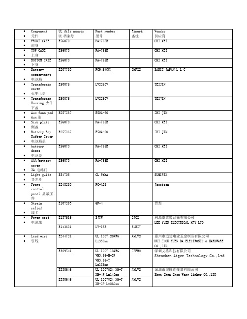
•Component •元件UL file numberUL档案号Part number型号Remark备注Vendor供应商•FRONT CASE•前身E56070 PA-765B CHI MEI•TOP CASE•上身E56070 PA-765B CHI MEI•BOTTOM CASE•下身E56070 PA-765B CHI MEI•Batterycompartment•电池箱E207780 PC945(GG) QMFZ2 SABIC JAPAN L L C•Transformercover•火牛上盖E50075 LV2250V TEIJIN•TransformerHousing 火牛下盖E50075 LV2250V TEIJIN•Aux foam pad•Aux盖E257267 E50A-60 ZHI JIN•Side plate•侧盖E56070 PA-765B CHI MEI•Battery BayRubber Cover•电池箱盖E257267 E50A-60 ZHI JIN•batterydoors•电池盖E56070 PA-765B CHI MEI•AAA batterycover•3A 电池门E56070 PA-765B CHI MEI•Light guide•导光片E54705 CL PMMA SUMIPEX•Frontcontrolpanel 显示压件E248280 PC+ABS Jacobson•Strainrelief•线卡E107293 6P-4 晋煜•Power cord •电源线E137516 SJTW ZJCZ 利源電業製品廠有限公司LEE YUEN ELECTRICAL MFY LTD. E143681 LY-13B ELBZ7•Lead wire •引线E244721 UL 1007 20AWGL=330mmAVLV2 惠州市远达电业五金制品有限公司HUI ZHOU YUEN DA ELECTRONIC & HARDWARECO.,LTDE329541 UL 1007 18AWGVH3.96-H-2PVH3.96-TL=186mmZPFW2 深圳艾格科技有限公司Shenzhen Aiger Technology Co.,LtdE330646 UL 1007#24 XH-TXH-4P L=140mmAVLV2 深圳市展旺连接器有限公司Shen Zhen Zhan Wang Linker CO.,LTDE330646 UL 1007#24 XH-TXH-2P L=260mmAVLV2E330646 UL 2547#28 PH-TPH-3P L=260mmAVLV2E330646 UL 2547#28 PH-TPH-3P L=220mmAVLV2E330646 UL 1185 22AWG XH-T XH-2P L=150mmAVLV2•Integralfuse •保险丝E340427 SFC0800A(800mA/250V FastActing Glass TubeFuse)JDYX 瑞卓电子(东莞)有限公司Dongguan Reomax Electronics Co., LTD•Fuse Holder •保险丝座E239034 H3(10A/250V)IZLT2 惠州市海牛電子有限公司HUIZHOU HINEW ELECTRIC APPLIANCE CO.,LTD.变压器材料清單/ MATERIAL LISTNO. MATERIAL DESCRIPTION Ul file MANUFACTURERS / SUPPLIERS1. 膠芯/Bobbin 最小0.71mm厚尼龍66 101(r9)一層minimum 0.71mm thick PA66101(r9) one layerUL:E41938 杜邦/E I Dupont De Nemours & Co Inc2 膠套/Shroud 最小0.50mm厚尼龍66 101(r9)一層minimum 0.50mm thick PA66101(r9) one layerUL:E41938 杜邦/E I Dupont De Nemours & Co Inc3 初級線圈PrimaryWinding 聚氨酯漆包線MW75C(130℃) 或Polyurethane Wire,MW75C(130℃)UL:E258125 河源天裕電子塑膠有限公司He Yuan Sky Wealth Electronic And PlasticCo Ltd.4 初級跨線絕緣Pri. windingcrossoverinsulation CT25聚脂膠紙/CT-25 Polyestertape厚度:0.05mm*2 層/Thickness:0.05mm*2 layersUL:E165111 靖江亞華壓敏黏膠有限公司Jingjiang Yahua Pressure Sensitive Glue COLTD5 溫度保險Thermal Fuse Type: A4-F130 Deg.C ( 250V/2A)UL:E140847 雅寶電子有限公司/Aupo Electronics Inc.6 初級引線Primary Leads UL-1672 AWG #22 VW-1 300V105Deg.CUL:E191230UL:E189674UL:E211048UL:E214859恒輝(香港)發展有限公司Ever Bright (Hongkong) development CompanyLimited.深圳东聚Shenzhen Dong Ju Wire & CableCo.,Ltd.琦富瑞Qifurui Electronics co阳泰氟电线电缆YANGTAI WIRE & CABLE CO LTD7 初級引線Primary Leads 聚氨酯漆包線MW75C(130℃) 或Polyurethane Wire,MW75C(130℃)or聚氨酯漆包線MW79C(155℃)Polyurethane Wire,MW79C(155℃)UL:E258125UL:E201757河源天裕電子塑膠有限公司He Yuan Sky Wealth Electronic And PlasticCo Ltd.太平洋電線電纜深圳公司Pacific ElectricWire&Cable(shenzhen)Co.,Ltd.8 次級引線SecondaryLeads UL-1015 AWG #20 VW-1 600V105Deg.CUL:E191230UL:E189674UL:E211048UL:E214859恒輝(香港)發展有限公司Ever Bright(Hongkong) development Company Limited.深圳东聚Shenzhen Dong Ju Wire & CableCo.,Ltd.琦富瑞Qifurui Electronics co阳泰氟电线电缆YANGTAI WIRE & CABLE CO LTD9 次級引線SecondaryLeads CT25聚脂膠紙/CT-25 Polyestertape厚度:0.05mm*3 層/UL:E165111 靖江亞華壓敏黏膠有限公司Jingjiang Yahua Pressure Sensitive Glue COLTD.Thickness:0.05mm*3 layers聚酯膠片型號:MYLAR EL21 0.25mm厚PET film Type:MYLAR EL21 0.25mmThickUL:E93687 杜邦帝人/ Dupont Teijin Films U S L P10 外層絕緣Outinsulation CT25聚脂膠紙/CT-25 Polyestertape厚度:0.05mm*3 層/Thickness:0.05mm*3 layers聚酯膠片型號:MYLAR EL21 0.25mm厚PET film Type:MYLAR EL21 0.25mmThickUL:E165111UL:E93687靖江亞華壓敏黏膠有限公司Jingjiang Yahua Pressure Sensitive Glue COLTD.杜邦帝人/ Dupont Teijin Films U S L P11 鐵芯片LaminationCore EI-57 硅鋼片(H18 黑) 片厚0.50,疊厚35.3+/-0.5mmEI-57 silicon steel sheet(H18black), thickness:0.50mm,depth thickness:35.3+/-0.5mmN/A 東莞東駿電器有限公司Dongguan Dongjun Electrical Appliances Co.,Ltd.12 安裝架/Bracket 冷軋板鍍鋅Cold rolled Steel with Zinc-coatedN/A 東莞駿豐五金製品廠Dongguan JunFeng MetalManufactory13 屏蔽殼/Endbell 冷軋板鍍鋅Cold rolled Steel with Zinc-coatedN/A 東莞駿豐五金製品廠Dongguan JunFeng MetalManufactory14 次級連接器Secondaryconnector Housing: JS-1121-02 & Terminal:JS-1121-THousing: A3963H-2P & Terminal:A3963-TPUL: E113875UL: E326732喬訊電子有限公司Chyao shiunn electronicIndustrial Ltd.長江連接器有限公司ChangJiang Connectors CoLtd15 浸漬/Impregnation Insulating Varnish/絕緣油Type: 8562/C, class FUL:E200154 恒昌化學塗料公司HANG CHEUNG PETROCHEMICALLTD。

徕卡M9主要参数数码相机类型:旁轴数码相机有效像素数:1800万液晶屏尺寸:2.5英寸存储卡类型:SD卡/SDHC卡快门速度:32-1/4000秒尺寸:139×37×80mm电源:锂离子充电电池(3.7VD...传感器类型:CCD最高分辩率:5212×3472微距对焦范围:视镜头而定快速定位:基本参数镜头闪光灯快门曝光控制拍摄性能取景及显示存储格式其他特性环境参数徕卡M9基本参数数码相机类型旁轴数码相机有效像素数1800万最大像素数1850万最高分辩率5212×3472传感器类型CCD对焦方式视镜头而定徕卡M9镜头实际焦距视镜头而定mm微距对焦范围视镜头而定光圈范围视镜头而定相机闪光灯内置徕卡M9快门快门类型电子控制焦平面快门、B门曝光模式程序自动曝光、手动曝光曝光测光多区矩阵测光,中央重点测光,点测光白平衡预设自动、7种预设,手动白平衡自拍功能支持12秒或2秒延时德语, 英语, 法语, 西班牙语, 意大利语, 日语, 简体中菜单语言文, 繁体中文, 俄语徕卡M9取景及显示液晶屏类型TFT LCD显示屏液晶屏象素23万徕卡M9存储格式存储卡类型SD卡/SDHC卡查看闪存卡报价锂电池、电池充电器、机身盖、USB连线、背带、随机附件CD-ROM、说明书连接类型USB 2.0颜色黑色, 银色重量585.0g三脚架螺孔1/4"标准徕卡M9环境参数工作湿度<85%存储温度-20-60℃以上参数仅供参考,产品以实物为准。
如参数不全或有误,欢迎您帮我们添加与纠正!>>位于德国索姆斯镇的徕卡股份公司(Leica Camera AG)推出了一款新的相机-- 徕卡M9,这是世界上第一台带全画幅24 ×36 mm传感器的联动测距数码相机。
作为世界上最紧凑的全画幅相机,徕卡M9沿承了徕卡联动测距系统和其他装置的传奇性传统。
在过去50多年中,徕卡不断采用最前沿的数字技术对M系列相机进行技术改进。

用于Peltier模块的集成温度控制器概论MAX1978 / MAX1979是用于Peltier热电冷却器(TEC)模块的最小, 最安全, 最精确完整的单芯片温度控制器。
片上功率FET和热控制环路电路可最大限度地减少外部元件, 同时保持高效率。
可选择的500kHz / 1MHz开关频率和独特的纹波消除方案可优化元件尺寸和效率, 同时降低噪声。
内部MOSFET的开关速度经过优化, 可降低噪声和EMI。
超低漂移斩波放大器可保持±0.001°C的温度稳定性。
直接控制输出电流而不是电压, 以消除电流浪涌。
独立的加热和冷却电流和电压限制提供最高水平的TEC保护。
MAX1978采用单电源供电, 通过在两个同步降压调节器的输出之间偏置TEC, 提供双极性±3A输出。
真正的双极性操作控制温度, 在低负载电流下没有“死区”或其他非线性。
当设定点非常接近自然操作点时, 控制系统不会捕获, 其中仅需要少量的加热或冷却。
模拟控制信号精确设置TEC 电流。
MAX1979提供高达6A的单极性输出。
提供斩波稳定的仪表放大器和高精度积分放大器, 以创建比例积分(PI)或比例积分微分(PID)控制器。
仪表放大器可以连接外部NTC或PTC热敏电阻, 热电偶或半导体温度传感器。
提供模拟输出以监控TEC温度和电流。
此外, 单独的过热和欠温输出表明当TEC温度超出范围时。
片上电压基准为热敏电阻桥提供偏置。
MAX1978 / MAX1979采用薄型48引脚薄型QFN-EP 封装, 工作在-40°C至+ 85°C温度范围。
采用外露金属焊盘的耐热增强型QFN-EP封装可最大限度地降低工作结温。
评估套件可用于加速设计。
应用光纤激光模块典型工作电路出现在数据手册的最后。
WDM, DWDM激光二极管温度控制光纤网络设备EDFA光放大器电信光纤接口ATE特征♦尺寸最小, 最安全, 最精确完整的单芯片控制器♦片上功率MOSFET-无外部FET♦电路占用面积<0.93in2♦回路高度<3mm♦温度稳定性为0.001°C♦集成精密积分器和斩波稳定运算放大器♦精确, 独立的加热和冷却电流限制♦通过直接控制TEC电流消除浪涌♦可调节差分TEC电压限制♦低纹波和低噪声设计♦TEC电流监视器♦温度监控器♦过温和欠温警报♦双极性±3A输出电流(MAX1978)♦单极性+ 6A输出电流(MAX1979)订购信息* EP =裸焊盘。

请参考本文档末的信息。
1.0 产品描述供货尺寸• 2 – 14英寸 IPS 管道尺寸• 63 – 355 毫米 ISO 管道尺寸管道材料• 符合 ASTM D3035 和 ASTM F714 或 ISO 4427-2 (SDR 7 – 26) 的 HDPE 管道• PE-RT 管道符合 ASTM D3035、单元分类 PE445574C、ASTM F2619 和 ASTM F714 (SDR 7 – 26) 标准• 有关交联聚乙烯(PE-Xa)管道的信息,请参见技术文件 36.01• 有关其他管道材料,请与 Victaulic(唯特利)联系最大工作压力• 达到或超过 HDPE 或 PE-RT 管道的额定压力工作温度• 视管道制造商额定值和密封垫圈选用而定• 有关密封垫圈性能选项,请参阅第 3.0 节• 有关管道材料性能极限,请咨询管道制造商功能• 连接平端HDPE管道• 采用 Installation-Ready™专利技术,无零散部件管道制备• 适用于平端 HDPE 或 PE-RT 管道注• 本文档中对 HDPE 的所有引用都包括 PE-RT2.0 CERTIFICATION/LISTINGS注• 有关详细信息,请参见技术文件 10.01:Victaulic(唯特利)消防认证参考指南。
• 有关详细信息,参见技术文件 02.06:Victaulic(唯特利)饮用水产品认证 – ANSI/NSF 61 和 ANSI/NSF 372。
• W aterMark™认证只适用于带 “E” 级三元乙丙橡胶(EPDM)密封垫圈的熔融粘结环氧树脂涂层卡箍。
有关进一步详细信息,请与 Victaulic(唯特利)联系。
用于HDPE管道的 Victaulic®(唯特利™)平端卡箍905 型19.07-CHI如需产品安装、维护或支持信息,3.0 规格 – 材料壳体:符合 ASTM A536之65-45-12 等级要求的球墨铸铁。

L6599高压谐振控制器特征⏹ 50%占空比,谐振半桥变频控制 ⏹ 高精度振荡器⏹ 高至500kHz 的工作频率 ⏹ 两级过流保护:变频和停机闭锁 ⏹ 与PFC 控制器的接口 ⏹ 自锁禁止输入 ⏹ 轻载脉冲工作模式⏹ 上电/断电顺序或欠压保护输入 ⏹ 单调输出电压上升为非线性软启动⏹ 整合了一个能够承受600V 以上电压的高压浮动结构和一个同步驱动式高压横向双扩散金属氧化物半导体(LDMOS)器件,节省了一个外部快速恢复自举二极管⏹ 用低电压下拉方式为两个栅驱动器提供一个输出电流0.3A 和灌入电流0.8A的典型峰值电流处理能力。
⏹ DIP-16,SO-16N 两种封装特征⏹ 液晶电视和等离子电视的电源 ⏹ 台式电脑和初级服务器 ⏹ 电信设备开关电源 ⏹ 交直流适配器的开关电源框图目录1 驱动描述 . . . . . . . . . . . . . . . . . . . . . . . . . . . . . . . . . . . . . . . . . . . . . . . . . .42 引脚设置 . . . . . . . . . . . . . . . . . . . . . . . . . . . . . . . . . . . . . . . . . . . . . . . . . .52.1 引脚排列 . . . . . . . . . . . . . . . . . . . . . . . . . . . . . . . . . . . . . . . . . . . . . . . . . . . .52.2 引脚功能说明 . . . . . . . . . . . . . . . . . . . . . . . . . . . . . . . . . . . . . . . . . . . . . . . . 53 典型系统框图 . . . . . . . . . . . . . . . . . . . . . . . . . . . . . . . . . . . . . . . . . . . . . . 74 电气数据 . . . . . . . . . . . . . . . . . . . . . . . . . . . . . . . . . . . . . . . . . . . . . . . . . . 74.1 极限参数 . . . . . . . . . . . . . . . . . . . . . . . . . . . . . . . . . . . . . . . . . . . . . . . . . . . . . .74.2 热相关数据 . . . . . . . . . . . . . . . . . . . . . . . . . . . . . . . . . . . . . . . . . . . . . . . . . . . . .85 电气参数 . . . . . . . . . . . . . . . . . . . . . . . . . . . . . . . . . . . . . . . . . . . . . . . . . . . 96 典型的电气性能 . . . . . . . . . . . . . . . . . . . . . . . . . . . . . . . . . . . . . . . . . . . . . .127 应用资料 . . . . . . . . . . . . . . . . . . . . . . . . . . . . . . . . . . . . . . . . . . . . . . . . . . . 157.1 振荡器 . . . . . . . . . . . . . . . . . . . . . . . . . . . . . . . . . . . . . . . . . . . . . . . . . . . . . . .167.2 工作在空载或非常轻的负载状态 . . . . . . . . . . . . . . . . . . . . . . . . . . . . . . . . . . .187.3 软启动 . . . . . . . . . . . . . . . . . . . . . . . . . . . . . . . . . . . . . . . . . . . . . . . . . . . . . . . .217.4 电流检测,过流保护和过载保护 . . . . . . . . . . . . . . . . . . . . . . . . . . . . . . . . . 237.5 闭锁关机 . . . . . . . . . . . . . . . . . . . . . . . . . . . . . . . . . . . . . . . . . . . . . . . . . . . . . .267.6 LINE检测功能 . . . . . . . . . . . . . . . . . . . . . . . . . . . . . . . . . . . . . . . . . . . . . . . . . .277.7 自举部分 . . . . . . . . . . . . . . . . . . . . . . . . . . . . . . . . . . . . . . . . . . . . . . . . . . . .287.8 应用实例 . . . . . . . . . . . . . . . . . . . . . . . . . . . . . . . . . . . . . . . . . . . . . . . . . . . . .298 封装外形尺寸 . . . . . . . . . . . . . . . . . . . . . . . . . . . . . . . . . . . . . . . . . . . . . . . . .9 修订记录 . . . . . . . . . . . . . . . . . . . . . . . . . . . . . . . . . . . . . . . . . . . . . . . . . . . .1 驱动描述L6599是一个用于谐振半桥拓扑电路的精确的双端控制器。


盘点美军特种部队现役装备的七款“手枪”M9 BerettaM9 BerettaM9贝雷塔(M9 Beretta)是一款9毫米手枪,它是由意大利军火制造厂商“贝雷塔”设计和制造,目前这款手枪已经取代了柯尔特(1911)作为美国军方标准配枪。
目前,“贝雷塔92F”已经成了“半自动9毫米手枪”的代名词,并且广泛配备于美军特种部队,包括:游骑兵,三角洲特种部队和海豹突击队。
升级版的M9A1配备了Picatinny附件滑轨,斜面弹匣和PVD涂层弹匣。
M9 Beretta规格:重量:2.56磅(满弹),长度:8.5英寸,枪管长度:4.9英寸,最大射程1800米,有效射程50m。
柯尔特M1911a1柯尔特M1911a1M1911式基于勃朗宁设计的M1905式手枪,于1911年定型为M1911式,自1890年代后期以来,柯尔特M1911的设计一直保持不变。
直到1923年美国斯普林菲尔德兵工厂对该枪进行了改进并取名M1911A1。
此后,柯尔特M119 / M119a1一直在美军服役,早期的三角洲特种部队就装备了柯尔特M1911a1这款手枪,虽然三角洲还使用了其他手枪,例如格洛克17s / 21s等,但柯尔特M119a1仍然是三角洲军械库中的王牌手枪。
M1911A1因为其优秀的性能,之后成为了美国陆军的专用配枪,之后枪械制造商对M119a1进行了修改,增加了瞄准器,握把,扳机和加长/双叠弹匣等各种改进。
虽然美军三角洲特种部队还使用了其它类型的手枪,例如格洛克17s / 21s等,但柯尔特M119a1一直都是是三角洲军械库中的王牌手枪。
柯尔特1911a1规格:外型尺寸长度:216毫米,枪管长度127毫米,重量2.43磅(空),弹夹容量:7发,有效范围75码,枪口初速度253米/秒,枪口动能502焦。
M45 MEU(SOC)手枪M45 MEU(SOC)手枪MEU(SOC)手枪是1911.45 ACP改进型手枪,是为美国海军特种部队专门研发的一款手枪。

格斗军刀概述本文章来源:主题名品网|高端名刀。
格斗军刀一般人称军刀,格斗刀并没附带工具,刀锋特别锋利,一般有放血齿及血沟。
一般用作近身格斗(CQC),一般以乌钢制。
现役美国陆军的M-9刺刀其实是MPBS多功能刺刀,其求生刀和格斗刀的功能,刃长17.9cm,而且M-9可作小斧头,锯,铁线cut钳及开瓶器。
刀套包含刀鞘及磨刀石。
USMC新所用的格斗刀附有枪扣,可作刺刀之用。
刀套包含刀鞘及磨刀石。
中国制M-9出口型多用途刺刀。
世界十大军刀一:KABAR1217在战时超过一百万把的1217把被制造出来,受到了广大的士兵的一致好评。
二:冷钢三美武士第一把批量生产的“三美”钢利刃。
排行榜上的后起之秀。
三美的意思就是三层,三美钢是一种专门制作高档日刀的钢材。
是专门为了制作刀锯而发明的,也是唯一一种制刀专用钢。
这种钢材的最大特色就是他是采用3种不同的钢材合成在刀上。
简单的比喻这种钢材就像一个三明治。
三美钢的中心是极其坚硬的高碳钢两侧各镶嵌了一块韧性和弹性都很好的不锈钢板。
三美钢之所以采用三层结构是因为,三美武士的刀刃部分非常坚硬,而且锋利!但是如果整个刀身都采用高硬度钢材,在严酷的使用过程中刀身有可能损坏!一把高档刀的钢材在强度高的基础上还必须具有很高的韧性,可以抗击侧面的压力。
所以才有了三美钢!三美钢的结构使这款三美武士在高硬度刀锋的同时(硬度可达到60以上),刀身也具有非常好的韧性,三美结构使这把刀的Tanto刀头增强了25%的强度。
可惜是tmd 日本货```三:BUCK夜鹰平刃刀的质量之优异是其他刀具所不能比拟的,刃口惊人的锋利!即便是柔软的传真纸也能横切成丝!美国特种部队人手一刀的全部配备着巴克的653和650,能被军方采用的刀具才是真正的好刀,这是胜过任何说明的。
刀身厚达6毫米,能胜任野外恶劣的环境。
刀身硬度58HRC。
刀身和刀柄浑为一体,刀柄为塑胶防滑设计,握在手里非常牢固!刀鞘为高强度工程塑料为内衬,外裹尼龙,握把上方有按扣。

CONTENTSIntroduction (1)What’s Included with MicroCom 900M? (1)Controls (2)Setup (2)Operation (3)Battery (3)Menu Settings (4)Device Specifications (6)Product Care and Maintenance (7)Product Support (7)License Information (8)Pliant Warranty Statement (9)INTRODUCTIONWe at Pliant Technologies want to thank you for purchasing MicroCom 900M. MicroCom 900M is a compact, economical wireless intercom system that operates in the 900MHz frequency band to provide excellent range and performance. The system features small, lightweight belt packs and provides excellent sound quality, ease-of-use, and long-life battery operation.In order to get the most out of your new MicroCom 900M, please take a few moments to read this manual completely so that you better understand the operation of this product. This document applies to model PMC-900M. For questions not addressed in this manual, feel free to contact the Pliant Technologies Customer Support Department.PRODUC T FEATURES WHAT’S INCLUDED WITH MICROCOM 900M?• Holster • Neck Strap• USB Charging CableOPTIONAL ACCESSORIES• Economical single-channel system • Simple to operate • Up to 5 full-duplex users• Unlimited listen-only users • 900MHz frequency band • Encrypted FHSS technology • Small and lightweight• Water-resistant construction • Long, 10-hour battery life • Low latency (less than 35 ms)• PAC-USB5-CHG: MicroCom 5-Port USB Charger • PAC-MC-5CASE: IP-67-rated hard travel case • PHS-SB11LE-DM: SmartBoom® LITE Single Ear Pliant headset with Dual Mini connector for MicroCom • PHS-SB110E-DM: SmartBoom PRO Single Ear Pliant headset with Dual Mini connector for MicroCom • PHS-SB210E-DM: SmartBoom PRO Dual Ear Pliant headset with Dual Mini connector for MicroCom• PHS-IEL-M: MicroCom in-ear headset, single ear, left only • PHS-IELPTT-M: MicroCom in-hear headset with push-to-talk (PTT) button, single ear, left only • PHS-LAV-DM: MicroCom lavalier microphone and eartube • PHS-LAVPTT-DM: MicroCom lavaliermicrophone and eartube with PTT button • PHS-HH-DM: MicroCom hardhat/helmet headsetCONTROLSSETUP1. Connect a headset to the belt pack. The belt pack headset connection supports dual miniand single mini headsets. Dual mini connectors can be inserted in either direction. Single mini connectors can be inserted in either port of the headset connection.2. Power on. Press and hold the POWER button for three (3) seconds, until the screen turns on.3. Select a Group. Press and hold the MODE button for 3 seconds, untilthe “GRP” symbol is blinking on the LCD. Then, use the VOLUME +/− buttons to select a group number from 0–51. Short-press MODE to save your selection and proceed to ID setting.Important: Radios must have the same group number to communicate.4. Select an ID. When “ID” begins to blink on the LCD, use the VOLUME+/− buttons to select an ID number. Press and hold MODE to save your selection and exit the menu.a. Pack IDs range from 00–05.b. One pack must always use the “00” ID and serve as the master packfor proper system function. “MR” designates the master pack on its LCD.c. Listen-only packs must use the “05” ID. You may duplicate ID “05” onmultiple belt packs if setting up listen-only users. (See “Receiving Mode Selection” on page 4 for more information about thatprocess.)Talk/State LED Charging LED Power Button Talk ButtonHeadset ConnectionUSB Charger ConnectionVolume +/–ButtonsMode Button LCD ScreenAntennaFigure 1: Group Edit ScreenFigure 2: ID Edit ScreenFigure 3: ID Edit Screen (Master ID)OPERATION• Talk - Use the TALK button to enable or disable talk for the device. This button changes with a single, short press. “TK” appears on the LCD when enabled.• Volume Up and Down - Use the + and − buttons to control the volume. “VOL” and a numerical value from 00–09 appear on the LCD when volume is adjusted.• LED Modes -»Left-hand Talk/State LED is blue and double blinks when logged in and single blinks when logged out.»Right-hand Charging LED is red when battery is low and also red when charging in progress.LED turns off when charging is complete.OPERATING MULTIPLE MICROCOM SY STEMS IN ONE LOC ATIONEach separate MicroCom system should use the same Group for all belt packs in that system. Pliant recommends that systems operating in proximity to one another set their Groups to be at least ten (10) values apart. For example, if one system is using Group 03, another system nearby should use Group 13.BATTERYThe rechargeable Lithium-ion battery is installed in the device. Plug the USB charging cable into the USB port to recharge the battery. The charging LED in the right top corner of the device will illuminate solid red while the battery is charging and will turn off once the battery is fully charged. The battery charge time is approximately 3.5 hours from empty. The belt pack may be used while charging, but doing so may lengthen battery charge time.MENU SETTINGSThe following settings are adjustable from the belt pack menu.To access the menu, press and hold the MODE button for 3 seconds, until the “GRP” symbol is blinking on the LCD. Then, short-press the MODE button the specified number of times to access the setting you wish to change. Once you have finished your changes, press and hold MODE to save your selection and exit the menu.• Side Tone On/Off - Side tone allows you to hear yourself while talking. Louder environments may require you to increase your side tone.»To adjust side tone, access the belt pack menu, then press the MODE button twice. When the “S_” value is blinking on the LCD, use the VOLUME +/− buttons to select an option from S0–S5.»“S0” is off. “S1” is the lowest side tone level. “S5” is the highest.»The default side tone setting is “S3.”• Receiving Mode Selection - This setting allows you to set the belt pack to full duplex mode (both receiving and transmitting) or set it to receive only (i.e., listen only, which disables the belt pack’s talk function).»To switch the receiving mode setting, access the belt pack menu, then press the MODE button three (3) times. When the “P_” value is blinking on the LCD, use the VOLUME +/−buttons to select between “PO” and “PF.”»“PO” is full duplex (both receiving and transmitting). This mode may only be used with pack IDs 00–04.»“PF” is receive only (i.e., listen only). This mode may be used with any pack ID, but if you wish to set up multiple listen-only users, you may do so by repeating ID “05” as needed, and setting each pack to “PF” mode. This is an exception to the rule that all belt packs must have a unique ID number.»The default mode setting is “PO.”• Microphone Sensitivity Level Control - Set microphone sensitivity based on your environment and headset capabilities. Louder environments may require you to reduce the mic sensitivity, while quieter environments may require you to increase it.»To adjust the mic sensitivity setting, access the belt pack menu, then press the MODE button four (4) times. When the “C_” value is blinking on the LCD, use the VOLUME +/− buttons to select an option from C 1–C5.»“C 1” is the lowest sensitivity level. “C5” is the highest.»The default microphone sensitivity level setting is “C 1.”• Audio Output High/Low - Higher audio output is recommended for louder environments.Changing the output setting here results in a gain increase or decrease of 3 dB.»To switch the audio output setting, access the belt pack menu, then press the MODE button five (5) times. When the “U_” value is blinking on the LCD, use the VOLUME +/− buttons toselect between “UL” and “UH.”»“UL” is audio output low. “UH” is audio output high.»The default audio output setting is “UL” (audio output low).MENU OPTIONS RECOMMENDED SET TINGS BY HE ADSE TThe following table provides recommended MicroCom settings for several common headset models.Menu Setting OptionsDescription Side Tone S0S1, S2, S3*, S4, S5Side Tone OffSide Tone Levels 1–5Receiving Mode PO*PFReceiving and Transmitting Mode Receive-Only Mode (Listen-Only)Mic Sensitivity Level C1*, C2, C3, C4, C5Mic Sensitivity Levels 1–5Audio Output LevelUL UH*Audio Output Low Audio Output High* Default Settings Noted with AsteriskHeadset Model Recommended SettingMic Sensitivity LevelAudio Output LevelHeadset with boom mic C1UH Headset with lavalier micC3UHDEVICE SPECIFICATIONSSpecification**DetailsRadio Frequency Type ISM 902–928 MHzRadio Interference ISM 900 MHz: FSK Modulation with Frequency HoppingVoice Codec16 bit / 16 KHzTx Max Output Power100 mWRx Sensitivity-95 dBmVoice Latency<35 msFrequency Channels78 channelsChannel Spacing 2 MHzData Rate 2 MbpsBattery Type Rechargeable 3.7 V, 1,100 mA Li-ion fixed batteryBattery Life Approx. 10 hoursPower Consumption Average10 mA at Class 1 (100 mW)Charge Type USB Micro, 5V 1–2AFrequency Response50 Hz - 7 kHzMaximum Full Duplex Users5Dimension / Weight98 mm (H) x 49 mm (W) x 17 mm (D) / 88 gDisplay7-segment LCD**Notice about Specifications: While Pliant Technologies makes every attempt to maintain the accuracy of the information contained in its product manuals, that information is subject to change without notice. Performance specifications included in this manual are design-centered specifications and are included for customer guidance and to facilitate system installation. Actual operating performance may vary. Manufacturer reserves the right to change specifications to reflect latest changes in technology and improvements at any time without notice.PRODUCT CARE AND MAINTENANCEClean using a soft, damp cloth.CAUTION: Do not use cleaners that contain solvents. Keep liquid and foreign objects out of the device openings. If the product is exposed to rain, gently wipe off all surfaces,cables, and cable connections as soon as possible and allow unit to dry before storing. PRODUCT SUPPORTPliant Technologies offers technical support via phone and email from 07:00 to 19:00 Central Time (UTC−06:00), Monday through Friday.1.844.475.4268 or +1.334.321.1160****************************************Visit for product support, documentation, and live chat for help. (Live chat available 08:00 to 17:00 Central Time (UTC−06:00), Monday through Friday.)RETURNING EQUIPMENT FOR REPAIR OR MAINTENANCEAll questions and/or requests for a Return Authorization Number should be directed to the CustomerServicedepartment(***************************************).Donotreturnany equipment directly to the factory without first obtaining a Return Material Authorization (RMA) Number. Obtaining a Return Material Authorization Number will ensure that your equipment is handled promptly.All shipments of Pliant products should be made via UPS, or the best available shipper, prepaid and insured. The equipment should be shipped in the original packing carton; if that is not available, use any suitable container that is rigid and of adequate size to surround the equipment with at least four inches of shock-absorbing material. All shipments should be sent to the following address and must include a Return Material Authorization Number:Pliant Technologies Customer Service DepartmentAttn: Return Material Authorization #205 Technology ParkwayAuburn, AL USA 36830-0500LICENSE INFORMATIONPLIANT TECHNOLOGIES MICROCOM™ FCC COMPLIANCE STATEMENT00004130 (FCCID: YJH-MC-11)00004130-B (FCCID: YJH-MCS-900)This equipment has been tested and found to comply with the limits for a Class B digital device, pursuant to Part 15 of the FCC Rules. These limits are designed to provide reasonable protection against harmful interference in a residential installation. This equipment generates, uses and can radiate radio frequency energy and, if not installed and used in accordance with the instructions, may cause harmful interference to radio communications. However, there is no guarantee that interference will not occur in a particular installation. If this equipment does cause harmful interference to radio or television reception, which can be determined by turning the equipment off and on, the user is encouraged to try to correct the interference by one of the following measures:• Reorient or relocate the receiving antenna.• Increase the separation between the equipment and receiver.• Connect the equipment into an outlet on a circuit different from that to which the receiver is connected.• Consult the dealer or an experienced radio/TV technician for help.C AUTIONModifications not expressly approved by the party responsible for compliance could void the user’s authority to operate the equipment.FCC Compliance Information: This device complies with Part 15 of the FCC Rules. Operation is subject to the following two conditions: (1) This device may not cause harmful interference, and (2) this device must accept any interference received, including interference that may cause undesired operation.IMPORTANT NOTEFCC RF Radiation Exposure Statement: This equipment complies with FCC RF radiation exposure limits set forth for an uncontrolled environment.The antennas used for this transmitter must be installed to provide a separation distance of atleast 5 mm from all persons and must not be co-located or operating in conjunction with any other antenna or transmitter.9 / 9PLIANT WARRANTY STATEMENTPART S LIMITED WARRANT YReplacement parts for Pliant Technologies, LLC products are warranted to be free from defects in materials and workmanship for 120 days from the date of sale to the end user.This warranty does not cover any defect, malfunction, or failure caused by circumstances beyond the control of Pliant Technologies, LLC, including but not limited to negligent operation, abuse, accident, failure to follow instructions in the Operating Manual, defective or improper associated equipment, attempts at modification and/or repair not authorized by Pliant Technologies, LLC, and shipping damage. Any damage done to a replacement part during its installation voids the warranty of the replacement part.This limited warranty is the sole and exclusive express warranty given with respect to PliantTechnologies, LLC products. It is the responsibility of the user to determine before purchase that this product is suitable for the user’s intended purpose. ANY AND ALL IMPLIED WARRANTIES,INCLUDING THE IMPLIED WARRANTY OF MERCHANTABILITY, ARE LIMITED TO THE DURATION OF THIS EXPRESS LIMITED WARRANTY. NEITHER PLIANT TECHNOLOGIES, LLC NOR ANY AUTHORIZED RESELLER WHO SELLS PLIANT PROFESSIONAL INTERCOM PRODUCTS IS LIABLE FOR INCIDENTAL OR CONSEQUENTIAL DAMAGES OF ANY KIND.CrewCom® and MicroCom™ products arewarranted to be free from defects in materials and workmanship for a period of two yearsfrom the date of sale to the end user, under the following conditions:• First year of warranty included with purchase.• Second year of warranty requires product registration on the Pliant website.Tempest® professional products carry a two-year product warranty.All headsets and accessories (including Pliant-branded batteries) carry a one-year warranty.The sole obligation of Pliant Technologies, LLC during the warranty period is to provide, without charge, parts and labor necessary to remedy covered defects appearing in products returned prepaid to Pliant Technologies, LLC. This warranty does not cover any defect,malfunction, or failure caused by circumstances beyond the control of Pliant Technologies, LLC, including but not limited to negligent operation, abuse, accident, failure to follow instructions in the Operating Manual, defective or improper associated equipment, attempts at modification and/or repair not authorized by Pliant Technologies, LLC, and shipping damage. Products with their serial numbers removed or effaced are not covered by this warranty. This limited warranty is the sole and exclusive express warranty given with respect to Pliant Technologies, LLC products. It is the responsibility of the user to determine before purchase that this product is suitable for the user’s intended purpose. ANY AND ALL IMPLIED WARRANTIES, INCLUDING THEIMPLIED WARRANTY OF MERCHANTABILITY, ARE LIMITED TO THE DURATION OF THISEXPRESS LIMITED WARRANTY. NEITHER PLIANT TECHNOLOGIES, LLC NOR ANY AUTHORIZED RESELLER WHO SELLS PLIANT PROFESSIONAL INTERCOM PRODUCTS IS LIABLE FORINCIDENTAL OR CONSEQUENTIAL DAMAGES OF ANY KIND.。

XN297L 系列产品说明书2.4GHz 单片高速无线收发芯片概述XN297L系列芯片是工作在2.400~2.483GHz世界通用ISM频段的单片无线收发芯片。
该芯片集成射频收发机、频率发生器、晶体振荡器、调制解调器等功能模块,并且支持一对多组网和带ACK的通信模式。
发射输出功率、工作频道以及通信数据率均可配置。
芯片已将多颗外围贴片阻容感器件集成到芯片内部。
主要特性1、功耗较低发射模式(2dBm)工作电流19mA;接收模式工作电流15mA;休眠电流2uA。
2、节省外围器件支持外围5个元器件,包括1颗晶振和4个贴片电容;支持双层或单层印制板设计,可以使用印制板微带天线;芯片自带部分链路层的通信协议;配置少量的参数寄存器,使用方便。
3、性能优异250K / 1M / 2M bps模式的接收灵敏度为-91 / -87 / -83dBm;发射输出功率最大可达13dBm;抗干扰性好,接收滤波器的邻道抑制度高,接收机选择性较好。
其它特性应用方案目录1 命名规则 (4)1.1 XN297L 命名规则 (4)1.2 XN297L 系列产品选择 (4)2 主要电特性 (4)3 极限最大额定值 (3)4 系统结构方框图 (4)5 引脚定义 (5)6 芯片工作状态 (6)6.1 休眠模式 (8)6.2 待机模式-I(STB1) (8)6.3 待机模式-III(STB3) (8)6.4 待机模式-II(STB2) (8)6.5 接收模式 (9)6.6 发射模式 (9)7 数据通信模式 (9)7.1 普通模式 (11)7.2 增强模式 (11)7.3 增强发送模式 (12)7.4 增强接收模式 (12)7.5 增强模式下的数据包识别 (13)7.6 增强模式下的PTX 和PRX 的时序图 (13)7.7 增强模式下的接收端一对多通信 (14)7.8 DATA F I F O (15)7.9 中断引脚 (16)8 SPI 控制接口 (16)8.1 SPI 指令格式 (16)8.2 SPI 时序 (18)9 控制寄存器 (20)10 数据包格式描述 (36)10.1 普通模式的数据包形式 (36)10.2 增强模式的数据包形式 (36)10.3 增强模式的ACK 包形式 (37)11 典型应用电路(参考) (37)12 封装尺寸 (38)13 联系方式 (39)1 命名规则1.1 XN297L 命名规则图1 X N297L系列芯片命名规则1.2 XN297L 系列产品选择表1 XN297L系列产品选择2 主要电特性表2 XN297L系列芯片主要电特性频道的接收灵敏度退化 2dB;发射信号调制精度(EVM)退化10%。
MICRO-K microminiature circular connectors are rugged yet lightweight - and meet or exceed the applicable requirements of MIL-DTL-83513. Applications include biomedical,instrumentation and miniature black boxes.MIK:Accommodate up to 55 contacts on .050(1.27) centers (equivalent to 420 contacts per square inch). Five keyway polarization prevents cross plugging. The threaded coupling nuts provide strong, reliable coupling. MIK recepta-cles can be either front or back panel mounted;in back mounting applications, panel thickness of up to 3/32" can be used on the larger sizes.Maximum temperature range - 55˚C to + 125˚C.Standard MIK connectors are available in two shell sizes accommodating two contact arrangements pre-wired to your specific requirements.MIKM:Similar to our MIK, except has a steel shell and receptacle for improved ruggedness and RFI resistance. It accommodates up to 85twist pin contacts. Maximum temperature range - 55˚C to + 125˚ C.MIKQ:A quick disconnect metal shell and receptacle version that can be instantaneously disconnected yet provides a solid lock when engaged. Applications include commercial TV cameras, portableradios, military gun sights, airborne landing systems and medical equipment. Maximum temperature range - 55˚C to +125˚C.SpecificationsSTANDARD MATERIAL AND FINISHESELECTRO/MECHANICAL FEATURES*For plug onlyElectrodeposited for receptacle.MIKThermoplastic Stainless Steel Passivated Glass-reinforced Thermoplastic 50Microinch Gold Plated Copper AlloyStainless Steel Stainless Steel Passivated Glass-reinforced Thermoplastic 50Microinch Gold Plated Copper AlloyBrass Brass, Electroless Nickel Plated*Glass-reinforced Thermoplastic 50Microinch Gold Plated Copper AlloyNo. of Contacts Wire SizeContact Termination Contact Rating Couping Polarization Contact Spacing Shell Styles 7,55#24 AWG thru #32 AWGCrimp 3Amps Threaded Keyways .050 (1.27)Centers0-Wall Mtg.6-Straight Plug7,55, 85#24 AWG thru #32 AWGCrimp 3Amps Threaded Keyways .050 (1.27)Centers 0-Wall Mtg.6-Straight Plug7,19, 37#24 AWG thru #32 AWGCrimp 3Amps Push/Pull Keyways .050 (1.27)Centers 7-Jam Nut 6-Straight Plug 9-Rear Panel Mtg. ReceptacleShellCoupling Nut Insulator ContactsMIKM MIKQ MIKMIKMMIKQ How to OrderSERIESMIK M 6-55P** ** * *SERIESMIK: Microminiature Circular7, 19, 37, 55, 85(H) 001 -18", 7/34 strand, #26 AWG,MIL-W-16878/4, Type E Teflon,yellow.18",7/34 strand, #26 AWG,MIL-W-16878/4, Type E Teflon,color coded to MIL-STD-681System I.1/2" uninsulated solid #25AWG gold plated copper.1" uninsulated solid #25 AWG gold plated copper.(H) 003 -(L)1-(L)2-G -Cable nut and grip (MIKQ plug only)N -Nut only (MIKQ plug only)NOTE: Contact types cannot be interchanged between shell styles.P -Pin S -SocketH -Insulated round hook-up wire L -Uninsulated round solid wireNo Letter - Screw couping, plastic shell M -Screw coupling, metal shell Q -Push/Pull, metal shell 0-Wall mounting receptacle (MIK and MIKM only)6-Straight plug (MIK, MIKM and MIKQ)7-Jam nut mount (MIKQ only)9-Rear panel mounted receptacle (MIKQ)CONNECTOR TYPESSHELL STYLESCONNECTOR TYPE SHELL STYLECONTACT ARRANGEMENT CONTACT ARRANGEMENTS CONTACT TYPE CONTACT TYPE TERMINATION TYPETERMINATION TYPESTERMINATION LENGTH CODE TERMINATION LENGTH CODE (STANDARDS)HARDWAREHARDWARERoHS COMPLIANCE RStandard Wire Termination CodesThe following termination codes are listed for your information. For additional codes please refer to Appendix on page 79 and 81. All wire lengths are minimum.HARNESS TYPES (H)#26 A WG per MIL-W-16878Type E,Teflon S tranded L ength020019026029028001038009010011013017042027016034025002003023004005006048046041 3(76.2)6(152.4)8(203.2)10(254.0)12(304.8)18(457.2)20(508.0)24(609.6)30(762.0)36(914.4)48(1219.2)72(1828.8)120(3048.0)-All Yell o w Co l o r Cod e dContact ArrangementsFace View, Pin Side-(Male Twist Pin Contacts)MIK/MIKM/MIKQ7Contacts394857473831535512MIKQ19 ContactsMIKQ37 ContactsMIK/MIKM55 ContactsMIKM85 ContactsCavity identification numbers are for reference only, they do not appear on connectors.Shell Dimensions.335 (8.51)Max.MIK (Rear Panel Mount Thickness - see Tabulation "T")Weight given is 1/2" uninsulated, solid #25 AWG gold plated copper pigtailsPlu g Rece p tacleS hell S i z e7onl yRece p tacleS hell S i z e55 onl yPlu gPlugPart Numberby Shell SizeMIK6-7PMIK6-55PAThreadDMax.LMax.Avg. Weightoz. (gm.) ±5%5/16-24UNF-2B9/16-24UNF-2A.375 (9.52).755 (19.18).315 (8.00).460 (11.68).054 (1.54).202 (5.72)Part Numberby Shell SizeMIK0-7SMIK0-55SAThreadD±.010 (0.25)FMax.H±.003 (0.08)K±.010 (0.25)LMax.R±.005 (0.13)SMax.TMax.Avg. Weightoz. (gm.) ± 5% 5/16-24UNF-2B9/16-24UNF-2A.325 (8.26).625 (15.88).315 (8.00).440 (11.18).078 (1.98).089 (2.26).062 (1.57).100 (2.54).355 (9.02).495 (12.57).460 (11.68).580 (14.73).630 (16.00).760 (19.30).032 (0.81).062 (1.57).022 (.635).134 (3.81) ReceptacleShell Dimensions (Continued)MIKM (Rear Panel Mount Thickness .335 (8.51) max. - see Tabulation "T")D ..335 (8M a D.PlugReceptacleShell Size 7 onlyReceptacle Receptacle Shell Size 55 & 85PlugPlugMIKM6-7P 5/16-24UNF-2A.375(9.52) .315 (8.00) .054 (1.54)MIKM6-55P 5/8-24UNEF-2B.775(19.18) .440 (11.18) .333 (9.44) MIKM6-85P 11/16-24UNEF-2B .860 (21.84).460 (11.68).419 (11.88)MIKM0-7S 5/16-24UNF-2A .325 (8.26).320 (8.13) .078 (1.98) .062 (1.57) .400 (10.16) .460 (11.68).630 (16.00) .032 (0.81) .051 (1.45) MIKM0-55S 5/8-24UNEF-2A .625 (15.88).440 (11.18) .091 (2.31) .062 (1.57) .490 (12.45) .580 (14.73) .760 (19.30) .125 (3.18) .269 (7.62)MIKM0-85S 11/16-24UNEF-2A .745 (18.92) .440 (11.18).091 (2.31).062 (1.57).490 (12.45) .674 (17.12) .845 (21.46) .125 (3.18) .346 (9.80)Part Numberby Shell SizePart Number by Shell SizeA ThreadD Max.L Max.Avg. Weightoz. (gm.)+_5%A ThreadDF Max.H +_.003 (0.08)K L Max.R +_.005 (0.13)SMax.T Max.Avg. Weight oz. (gm.)+_5%MIKQ6-7S .385(9.78) .305 (7.75) .180 (4.57) .214 (6.08)MIKQ6-19S .515(13.08) .405 (10.29) .260 (6.60) .376 (10.70)MIKQ6-37S.760 (19.30).635 (16.13).350 (8.89).714 (20.23)MIKQ6-7S .510(12.95) .245 (6.22) .359 (9.12) 3/8-32UNEF-2A .128 (3.63)MIKQ7-37P.855(21.71).520 (13.20).740 (18.80)3/4-20UNEF-2A.300 (8.52)MIKQ (Front Panel Mounting Type Shown-.093 (2.36) Thickness)C .043±.005 C DIM.ACROSS FLA TPlugPlugReceptacle Receptacle*Std. Conn. not supplied with Cable Nut & Grip, See Mod Codes. Lanyard Relase Is Available. Consult factory.Part Number by Shell Size A MAX.B MAX.C Ref.Avg. Weight oz. (gm.)±5%Part Number by Shell Size A MAX.B MAX.C MAX.D Thread Avg. Weightoz. (gm.)±5%Front Panel Mounting-MIKQ7MIKQ Front Panel MountingMIKQ7-7P .364(9.24) .390 (9.91)MIKQ7-19P .475(12.06) .515 (13.08)MIKQ7-37P .740(18.78) .755 (19.17)Shell SizeA ±.005 (0.13)BDIA.Shell Dimensions (Continued)MIKQ9-7P (Back Panel Mounting)MIKQ9-19P (Back Panel Mounting)MIKQ9-37P (Back Panel Mounting)MIKQ Rear Panel MountingReceptacleReceptacleReceptacleRear Panel Mounting-MIKQ9Shell SizeMIKQ9-7PMIKQ9-19PMIKQ9-37P.425 (10.76).535 (13.58).740 (18.78).485 (12.32)MAX..250 ± .010WIREEXTENSIONLENGTH.250 ± .010 (6.35 ± 0.25).485 (12.32) MAX..440 (11.18).564 (14.33).755 (19.17)A±.005 (0.13)BDia.。