MA4E2513L-1289W中文资料
- 格式:pdf
- 大小:93.02 KB
- 文档页数:3
2014年11月伺服驱动编码器有关所有可用接口的全面说明和一般电气信息,参见海德汉编码器接口样本,ID 1078628-xx。
本样本是以前样本的替代版,所有以前版本均不再有效。
订购海德汉公司的产品仅以订购时有效的样本为准。
产品遵循的标准(ISO,EN等),请见样本中的标注。
本样本不是海德汉公司全线产品的介绍。
只适用于选择伺服驱动编码器。
选型表是关于海德汉公司所有电机驱动编码器的概要信息以及最重要的技术参数信息。
技术特性说明是关于电机驱动旋转编码器、角度编码器和直线光栅尺的基本信息。
有关安装信息和详细技术参数,参见专为驱动技术开发的旋转编码器。
其它旋转编码器信息,参见其单独产品样本。
有关选型表中直线光栅尺和角度编码器的安装、技术参数和尺寸信息,详见相应的产品样本。
样本旋转编码器产品概要电梯行业的旋转编码器样本直线光栅尺用于NC数控机床样本敞开式直线光栅尺产品概要应用于有爆炸危险环境中的旋转编码器样本内置轴承角度编码器样本无内置轴承角度编码器样本模块式磁栅编码器August 2012Längenmessgerätefür gesteuerteWerkzeugmaschinen März 2012OffeneL Januar 2009ProduktübersichtDrehgeberfür explosionsgefährdeteBereiche (ATEX)August 2013Winkelmessgerätemit EigenlagerungSeptember 2012MagnetischeE目录4伺服驱动编码器伺服驱动的控制系统需要测量系统提供位置和速度控制单元所需的反馈信息和电子换向信号。
编码器性能对电机的重要特性具有决定性影响,例如: •定位精度 •速度稳定性•带宽,它决定对驱动指令信号的响应速度和抗干扰性能 •功率损失 •尺寸 •噪音 •安全数字位置和速度控制系统海德汉公司为旋转电机和直线电机提供所需的全面产品:•带或不带换向刻轨的增量式旋转编码器和绝对式旋转编码器 •增量式和绝对式角度编码器 •增量式和绝对式直线光栅尺 •增量式模块型编码器旋转编码器5旋转编码器“数字”驱动系统的电机(数字位置和速度控制)本样本中的所有海德汉编码器都具有方便电机制造商安装和接线的特点,而且安装和接线成本低。
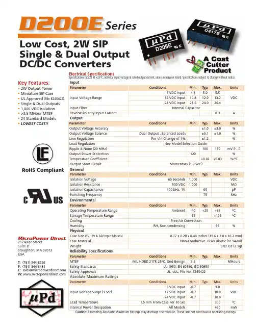
MicroPower Direct292 Page StreetSuite DStoughton, MA 02072USAT: (781) 344-8226F: (781) 344-8481E: sales@ W: RoHS CompliantKey Features:• 2W Output Power • Miniature SIP Case• UL Approved (File E245422)• Single & Dual Outputs • 1,000 VDC Isolation • >3.5 MHour MTBF • 24 Standard Models •LOWEST COST!!D200E Low Cost, 2W SIPSingle & Dual Output DC/DC Con v ert e rsSeriesInputParameterConditionsMin.Typ.Max.UnitsInput Voltage Range 5 VDC Input 4.5 5.0 5.5VDC 12 VDC Input 10.812.013.224 VDC Input21.624.026.4Input FilterInternal CapacitorReverse Polarity Input Current0.3A OutputParameterConditionsMin.Typ.Max.Units Output Voltage Accuracy ±1.0±3.0%Output Voltage Balance Dual Output , Balanced Loads±0.1±1.0%Line Regulation For Vin Change of 1%±1.2%Load Regulation See Model Selection GuideRipple & Noise (20 MHz)100150mV P - P Output Power Protection 120%Temperature Coeffi cient ±0.02±0.03%/ºC Output Short CircuitMomentary (1.0 Sec.)GeneralParameter ConditionsMin.Typ.Max.Units Isolation Voltage 60 Seconds 1,000VDC Isolation Resistance 500 VDC 1,000M ΩIsolation Capacitance 100 kHz, 1V60pF Switching Frequency75kHz EnvironmentalParameterConditionsMin.Typ.Max.Units Operating Temperature Range Ambient-40+25+85ºC Storage Temperature Range -55+125ºCCooling Free Air ConvectionHumidityRH, Non-condensing95%PhysicalCase Size (5V 12V & 24V Input Models)0.77 x 0.28 x 0.40 Inches (19.6 x 7.0 x 10.2 mm)Case Material Non-Conductive Black Plastic (UL94-V0)Weight0.07 Oz (2.1g)Reliability Specifi cationsParameter ConditionsMin.Typ.Max.Units MTBFMIL HDBK 217F , 25ºC, Gnd Benign3.5MHoursSafety Standards UL 1950, EN 60950, IEC 60950Safety ApprovalsUL, cUL; File No. E245422Absolute Maximum RatingsParameterConditionsMin.Typ.Max.UnitsInput Voltage Surge (1 Sec) 5 VDC Input -0.79.0VDC 12 VDC Input -0.718.024 VDC Input-0.730.0Lead Temperature 1.5 mm From Case For 10 Sec300ºC Internal Power DissipationAll Models450mW Caution: Exceeding Absolute Maximum Ratings may damage the module. These are not continuous operating ratings.Electrical Specifi cationsSpecifi cations typical @ +25°C, nominal input voltage & rated output current, unless otherwise noted. Specifi cations subject to change without notice.Notes:• All dimensions are typical in inches (mm)• Tolerance x.xx = ±0.01 (±0.25)• Pin 1 is marked by a “dot” or indentation on the side of the unitModel Number InputOutput LoadRegulation (%, Max) Effi ciency(%, Typ)Fuse Rating Slow-Blow (mA)Voltage (VDC)Current (mA)Voltage (VDC)Current (mA, Max)Current(mA, Min)Nominal RangeFull-Load No-LoadD201E 5 4.5 - 5.549430 5.0400.040.015811,000D202E 5 4.5 - 5.5488309.0222.023.015821,000D203E 5 4.5 - 5.54763012.0167.017.015841,000D204E 5 4.5 - 5.54763015.0133.014.015841,000D205E 5 4.5 - 5.548830±5.0±200.0±20.015821,000D206E 5 4.5 - 5.548230±9.0±111.0±12.015831,000D207E 5 4.5 - 5.547030±12.0±83.0±9.015851,000D208E 5 4.5 - 5.547030±15.0±67.0±7.015851,000D211E 1210.8 - 13.220315 5.0400.040.01582500D212E 1210.8 - 13.2201159.0222.023.01583500D213E 1210.8 - 13.21961512.0167.017.01585500D214E 1210.8 - 13.21961515.0133.014.01585500D215E 1210.8 - 13.220115±5.0±200.0±20.01583500D216E 1210.8 - 13.219815±9.0±111.0±12.01584500D217E 1210.8 - 13.219415±12.0±83.0±9.01586500D218E 1210.8 - 13.219415±15.0±67.0±7.01586500D221E 2421.6 - 26.41008 5.0400.040.01583200D222E 2421.6 - 26.49989.0222.023.01584200D223E 2421.6 - 26.497812.0167.017.01586200D224E 2421.6 - 26.497815.0133.014.01586200D225E 2421.6 - 26.4998±5.0±200.0±20.01584200D226E 2421.6 - 26.4988±9.0±111.0±12.01585200D227E 2421.6 - 26.4968±12.0±83.0±9.01587200D228E2421.6 - 26.4968±15.0±67.0±7.01587200Pin Single Dual Pin Single Dual 1+Vin +Vin 5No Pin Common 2-Vin -Vin 6+Vout+Vout4-Vout-VoutDerating Curve gNotes:1. Output load regulation is specifi ed for a load change of 10% to 100%.2. T hese units should not be operated with a load under 10% of full load. Operation at no-load may cause damage to the unit.3. These converters will operate without external components. However, when measuring output ripple, it is recommended that an external ceramic capacitor be placed from the +Vout pin to the -Vout pin for single output units and from each out-put to common for dual output units. An input capacitor will enhance stability over temperature and input line variations. Recommended capacitor values are given in the table below. For applications requiring very low output noise levels, a simple LC fi lter should be effective.4. D ual output units may be connected to provide a 10V, 18V, 24V or 30 VDC output. To do this, connect the load across the posi-tive (+Vout) and negative (-Vout) outputs and fl oat the output common5. It is recommended that a fuse be used on the input of a power supply for protection. See the Model Selection table above forthe correct rating.Vin InputCapacitor VoutOutput Capacitor Single Dual5 VDC 4.7 µF 5 VDC 10.0 µF 4.7 µF 12 VDC 2.2 µF 9 VDC 4.7 µF 2.2 µF 24 VDC 1.0 µF 12 VDC 2.2 µF 1.0 µF15 VDC 1.0 µF 0.47 µF MicroPower Direct292 Page Street Ste D Stoughton, MA 02072 • TEL: (781) 344-8226 • FAX: (781) 344-8481 • E-Mail: sales@Model Selection GuideMechanical DimensionsPin Connections。
内策尔容栅编码器参数全文共四篇示例,供读者参考第一篇示例:内策尔容栅编码器是一种常用的位置传感器,它可以将位置信息转换为数字信号,从而实现机械设备的精准定位和控制。
内策尔容栅编码器参数是指编码器的性能指标和技术参数,对于用户选型和使用具有重要意义。
下面我们将详细介绍内策尔容栅编码器的参数及其含义。
内策尔容栅编码器的分辨率是一个重要的参数。
分辨率是指编码器每旋转一周所能输出的脉冲数,通常以PPR(脉冲每圈)或CPR(脉冲计数数)为单位来表示。
分辨率越高,编码器的精度和分辨率就越高。
一般来说,内策尔容栅编码器的分辨率可以根据用户的需求进行选择,常见的分辨率有100、200、500、1000、2000等。
内策尔容栅编码器的工作电压是另一个重要参数。
工作电压是指编码器工作时所需要的电压范围,通常为DC5V、DC12V、DC24V等。
选择适合的工作电压可以确保编码器正常工作并提高其稳定性和可靠性。
内策尔容栅编码器的输出信号类型也是需要考虑的参数之一。
输出信号类型主要有两种,一种是模拟输出信号(如模拟电压和模拟电流),另一种是数字输出信号(如脉冲信号或数字串口信号)。
根据用户的需求和实际应用情况选择合适的输出信号类型可以更方便地与控制器或PLC进行连接。
内策尔容栅编码器的安装方式也是一个重要参数。
安装方式主要包括法兰式安装、轴端式安装、吸附式安装等。
不同的安装方式适用于不同的机械结构和空间限制,用户在选择编码器时需要结合实际情况进行合理选择。
内策尔容栅编码器的防护等级和环境温度也是需要注意的参数。
防护等级是指编码器对尘土、湿气、震动等外界环境的抵抗能力,通常使用IP等级来表示,如IP65、IP67等。
用户在选择时需要根据工作环境的特点来选择合适的防护等级。
编码器的工作环境温度也需要考虑,一般标准的工作温度范围为-10℃~+60℃,用户需要根据实际情况选择适合的编码器。
内策尔容栅编码器的参数是用户选择和应用时需要考虑的关键因素,合理的选择和配置可以提高机械设备的精度和稳定性,从而提高生产效率和品质。
LAUREL ELECTRONICS, INC.4-20 mA & Serial Output Transmitter for Resistance Input in OhmsFeatures•4-20 mA, 0-20 mA, 0-10V or -10V to +10V transmitter output, 16 bits, isolated•RS232 or RS485 serial data output, Modbus or Laurel ASCII protocol, isolated•Dual 120 mA solid state relays for alarm or control, isolated•Five precalibrated resistance input ranges from 20.000 Ω to 200.00 kΩ•Fixed 2.0000 ohm, 2.0000 MΩ and 20.000 MΩ range available as a factory specia• 1 mΩ resolution on 20 Ω scale•Custom curve linearization for changing resistance transducers•2, 3 or 4-wire connection with lead resistance compensation•Analog output resolution 0.0015% of span (16 bits), accuracy ±0.02% of span•DIN rail mount housing only 22.5 mm wide, detachable screw-clamp connectors•Universal 85-264 Vac / 90-300 Vdc or 10-48 Vdc / 12-32 Vac powerDescriptionThe Laureate Resistance Transmitter is factory calibrated forfive jumper selectable resistance ranges from 20 Ω to 200 kΩ.Fixed factory-special ranges of 2.000 Ω, 2.0000 MΩ and 20.000MΩ are also available. Accuracy is an exceptional 0.01% of fullscale ± 2 counts. Resolution is one part in 20,000. In the 20 Ωrange, resolution is 1 mΩ, making the transmitter suitable forcontact resistance and conductance measurements.Transmitter connections can be via 2, 3 or 4 wires. With 4-wirehookup, 2 wires are used for excitation and two separate wiresare used to sense the voltage across the resistance to bemeasured, thereby eliminating any lead resistance effects. With3-wire hookup, the transmitter senses the combined voltage dropacross the RTD plus two excitation leads. It also senses thevoltage drop across one excitation lead, and then subtracts twicethis voltage from the combined total. This technique effectivelysubtracts the lead resistance if the excitation leads are the same.All resistance ranges are digitally calibrated at the factory, withcalibration factors stored in EEPROM on the signal conditionerboard. This allows ranges and signal conditioner boards to bechanged in the field without recalibrating the transmitter. Ifdesired, the transmitter can easily be calibrated using externalstandards plus scale and offset in software.Fast read rate at up to 50 or 60 conversions per second whileintegrating the signal over a full power line cycle is provided byConcurrent Slope (Pat 5,262,780) analog-to-digital conversion.High read rate is ideal for peak or valley capture and for real-timecomputer interface and control.Open sensor indication is standard and may be set up to indi-cate either upscale or downscale. Excitation is provided by thetransmitter.Custom curve linearization, available with the Extendedversion, makes this transmitter ideal for use with transducerswhose output is a changing resistance.Standard features of Laureate transmitters include:•4-20 mA, 0-10V or -10V to +10V analog transmitter output,isolated, jumper-selectable and user scalable. All selectionsprovide 16-bit (0.0015%) resolution of output span and 0.02%output accuracy of a reading from -99,999 to +99,999 countsthat is also transmitted digitally. Output isolation from signaland power grounds eliminates potential ground loop problems.•Serial communications output, isolated. User selectableRS232 or RS485, half or full duplex. Three protocols are userselectable: Modbus RTU, Modbus ASCII, or Laurel ASCII.Modbus operation is fully compliant with Modbus Over SerialLine Specification V1.0 (2002). The Laurel ASCII protocolallows up to 31 Laureate devices to be addressed on thesame RS485 data line. It is simpler than the Modbus protocoland is recommended when all devices are Laureates.•Dual solid state relays, isolated. Available for local alarm orcontrol. Rated 120 mA at 130 Vac or 170 Vdc.•Universal 85-264 Vac power. Low-voltage 10-48 Vdc or 12-32 Vac power is optional.Easy Transmitter programming is via Laurel's InstrumentSetup Software, which runs on a PC under MS Windows. Thissoftware can be downloaded from this website at no charge. Therequired transmitter-to-PC interface cable is available from Laurel(P/N CBL04).SpecificationsRange Resolution Accuracy Excitation Current0-2.0000 Ω 0-20.000 Ω 0-200.00 Ω 0-2000.0 Ω 0-20000 Ω 0-200.00 kΩ 0-2.0000 MΩ 0-20.000 MΩ 0.1 mΩ1 mΩ10 mΩ100 mΩ1 Ω10 Ω100 Ω1 kΩ±0.01% of range± 2 counts5 mA5 mA500 µA50 µA5 µA500 nA500 nA75 nASignal InputInput Resolution Input Accuracy Update Rate, Max 16 bits (65,536 steps)±0.01% of full scale ± 2 counts 50/sec at 50 Hz, 60/sec at 60 HzAnalog Output (standard)Output Levels Compliance at 20 mA Compliance at 10V Output Resolution Output Accuracy Output Isolation 4-20 mA, 0-20 mA, 0-10 Vdc, -10 to +10Vdc (user selectable) 10V (0-500Ω load)2 mA (5 kΩ load or higher)16 bits (65,536 steps)0.02% of output span plus conversion accuracy250V rms working, 2.3 kV rms per 1 minute testSerial Communications (standard)Signal TypesData RatesOutput Isolation Serial Protocols Modbus Modes Modbus Compliance Digital Addressing RS232 or RS485 (half or full duplex)300, 600, 1200, 2400, 4800, 9600, 19200 baud250V rms working, 2.3 kV rms per 1 min testModbus RTU, Modbus ASCII, Laurel ASCIIRTU or ASCIIModbus over Serial Line Specification V1.0 (2002)247 Modbus addresses. Up to 32 devices on an RS485 line w/o a repeater.Dual Relay Output (standard)Relay Type Load Rating Two solid state relays, SPST, normally open, Form A 120 mA at 140 Vac or 180 VdcPower InputStandard Power Low Power Option Power Frequency Power Isolation Power Consumption 85-264 Vac or 90-300 Vdc10-48 Vdc or 12-32 VacDC or 47-63 Hz250V rms working, 2.3 kV rms per 1 min test 2W typical, 3W with max excitation outputMechanicalDimensions MountingElectrical Connections 129 x 104 x 22.5 mm case35 mm rail per DIN EN 50022 Plug-in screw-clamp connectorsEnvironmentalOperating Temperature Storage Temperature Relative Humidity Cooling Required 0°C to 55°C-40°C to 85°C95% at 40°C, non-condensingMount transmitters with ventilation holes at top and bottom. Leave 6 mm (1/4") between transmitters, or force air with a fan.PinoutMechanicalQA Application with Relays in Passband ModeA deviation limit (50 mΩ in this example) is set uparound both sides of a setpoint. The relay closes (oropens) when the reading falls within the deviationband, and opens (or closes) when the reading fallsoutside of this band. This mode sets up a passbandaround the setpoint and can be used for contactresistance testing in a production environment.RTD HookupIn 4-wire hookup, different pairs of leads are used to apply the excitation current and sense the voltage drop across the unknown resistance, so that the IR drop across the excitation leads is not a factor.In 3-wire hookup, the transmitter senses the combined voltage drop across the unknown resistance plus two excitation leads. It also senses the voltage drop across one excitation lead, and then subtracts twice this voltage from the combined total. This technique effectively subtracts all lead resistance and compen-sates for ambient temperature changes if the two excitation leads are identical.In 2-wire hookup, the transmitter senses the combined voltage drop across the unknown resistance and both lead wires. The voltage drop across the lead wires can be measured by shorting out the resistance during transmitter setup, and this voltage is then automatically subtracted from the combined total. However, changing resistance of the lead wires due to ambient tempera-ture changes will not be compensated.Ordering GuideCreate a model a model number in this format: LT20R1Transmitter Type LT Laureate 4-20 mA & RS232/RS485 output transmitter Main Board 2 Standard Main BoardPower0 Isolated 85-264 Vac or 90-300 Vdc 1 Isolated 10-48 Vdc or 12-32 VacResistance RangeR0 0-20 ohms (factory special fixed range) R1 0-20 ohms R2 0-200 ohms R3 0-2 kohms R4 0-20 kohms R5 0-200 kohmsR6 0-2 Mohms (factory special fixed range) R7 0-20 Mohms (factory special fixed range)Note: The same signal conditioner board can be used for resistance and RTD temperature measurement.AccessoriesCBL04 RS232 cable, 7ft. Connects RS232 screw terminals of LT transmitter to DB9port of PC.CBL02 USB to RS232 adapter cable. Combination of CBL02 and CBL04 connectstransmitter RS232 terminals to PC USB port.。
CB 45°45°450-687-9199 / 1-866-979-5999450-687-8477 / 1-866-421-8477 37Model 5138Colour: R204WModel 5143Colour: R205WModel 5134Colour: R204W Model 5133Colour: R204WModel 5132Colour: R204WWine RacksCIRCLE SHAPEDSPECIFICATIONS• If models 5132 and 5133 are paired together, it must bes pecified when placing your order.• Minimum size: 5132: 76.2 mm (3") height 5133: 69.8 mm (2 3⁄4") heightSPECIFICATIONSOpening size: 101.6 x 101.6 mm (4" x 4")SPECIFICATIONS1) Standard Hole Diameter: 101.6 mm (4")2) Distance between holes: 133.4 mm (5 1⁄4")3) A = [Width – (number of holes – 1) x 133.4 mm] ÷ 2 [Width – (number of hole – 1) x 5 1⁄4"] ÷ 2B = [Height – (number of hole – 1) x 133,4 mm] ÷ 2 [Height – (number of hole – 1) x 5 1⁄4"] ÷ 24) A or B minimum size: 76.2 mm (3")Model 5141Colour: R205W Model 5142Colour:R205W X SHAPED38 450-687-9199 / 1-866-979-5999450-687-8477 / 1-866-421-8477SERIE 69006507660765096609690769096505660569106912manufactured with 09 interior profile.Model 4106SPECIFICATIONS1) For special mullion frames (except series 6900) where the mullion bars line-up h orizontally,the door widths must be identical.2) An interior profile must be specified for models 000, 911, 912 (profile 09 by default) and910 (profile 151 by default) frame or mullion doors.3) Series 83 to 89 are only available in special mullion door models 6706, 6708, 6909 and 6912. This restrictiondoes not apply to series 93 to 99.4) Models 928, 942, 943 and 944 are available only in 4100 series.5) Model 996 frame and mullion doors are available only in 4100 series.6) Mitre style models 7730-31-32, 7930-31-32 and 928 are not available with glass retainerinsert grooves.COLOURS AVAILABLE• Clear (5351)• White (5350)Minimum sizesLites Height x Widthmm inches01 203.2 x 203.2 8 x 802 279.4 x 203.2 11 x 803 368.3 x 203.2 14 1⁄2 x 804 279.4 x 279.4 11 x 11 06 368.3 x 279.4 14 1⁄2 x 11 08 457.2 x 279.4 18 x 11 10 546.1 x 279.4 21 1⁄2 x 11 12 635.0 x 279.4 25 x 11GLASS INSTALLATION450-687-9199 / 1-866-979-5999450-687-8477 / 1-866-421-8477 41INSTALLATION Model 741Model 745Model 746Model 751Model 743Model 5718Model 5719Model 756Model 757Model 721SPECIFICATIONNailing strips should be glued and clamped rather than nailed.METHOD 1METHOD 242 450-687-9199 / 1-866-979-5999450-687-8477 / 1-866-421-8477 SPECIFICATIONS1) Only the bottom edge is p rofiled. Please specify the edge profile.2) Rosettes are centered v ertically in the A dimension and horizontally in the E dimension.3) Woodgrain pattern is parallel to width. (Certain exeptions may apply, please contact a Customer Sevice Representative for further information.)> 203.2 mm (8"), 5610 plain101.6 4 330.2 135611 with 2 routed circles 101.6 4 330.2 135616 with 2 applied rosette 101.6 4 330.2 135620 plain101.6 4 304.8 125621 with 2 routed circles 101.6 4 304.8 125626 with 2 applied rosette 101.6 4 304.8 125630 plain101.6 4 304.8 125631 with 2 routed circles 101.6 4 304.8 125636 with 2 applied rosette 101.6 4 304.8 125640 plain 101.6 4 254 105650 plain 101.6 4 152.4 63" Radius Corners Shaker Filler450-687-9199 / 1-866-979-5999 450-687-8477 / 1-866-421-8477 43I IT IHeatshield fillers are higher heat resistant fillers for kitchen c abinet installations where heat sources are ac oncern.HPL Heatshield fillers are pretested to temperatures above 120 °C (250 °F) without delamination, theHPL Heatshield Fillers are postformed 180° profiled components.Produced with compatible HPL, they are available in most colours. Please contact a Customer ServiceRepresentative for an up-to-date list of available colours.Heatshield Fillersedgebanding machines operating tandard edgebanding machines run at 88 °C (190 °F) to 99 °C (210 °F), we also offer PVC edgebanding which can be applied with the standard machines. Available finishes for each type of edgebanding are listed in the If A or B sizes are between: 101.6 mm (4") – 152.4 mm (6"), R = 101.6 mm (4")152.4 mm (6") – 203.2 mm (8"), R = 152.4 mm (6")203.2 mm (8") – 254 mm (10"), R = 203.2 mm (8")254 mm (10") – 381 mm (15"), R = 254 mm (10")NOTE: Minimum size for A and Bis 89 mm (3 ½")Corner ShelvesSHELF WITH RADIUSSHELF WITH ELLIPSEIf A R If A R Model 5120Model 5121Thermoplastic 1.2 m x 2.4 m (4’ x 8’) (5040)Laminated Panels – Unilam 5011 : 15.86 mm x 1.2 m x 2.7 m (5/8’’ x 4’ x 9’)5013 : 15.86 mm x 1.2 m x 2.4 m (5/8’’ x 4’ x 8’)5015 : 19.05 mm x 1.2 m x 2.4 m (3/4’’ x 4’ x 8’)NOTE: Available same colour back.1. 2. Duration3. Exclusions4.5.6.Starting on January 1 2011 (see conditions on reverse)DistributorInvoice #Date of purchaseY E A R SCERTIFICATE OFWARRANTYAPPLICABLE TO THERMOPLASTIC PRODUCTSPrémoulé supports05/20 BRPOLYDOORCDNServing you across North AmericaCANADAT 450-687-9199 / 1-866-979-5999F 450-687-8477 / 1-866-421-8477*************************Distributed byVisit our website and try our step-by-step quick and simple web module under the Cabinet Doors Section。
SOU-2cos φ ≥ 0.95M M HAL.230VKM MAC12250V / 1ADC14x AC1250V / 8AAC13xAC2250V / 5AAC14250V / 4AAC3250V / 4AAC15250V / 3AAC5b250WDC530V / 2AAC6a250V /4ADC1230V / 8AAC7b250V / 1ADC1330V / 2A02-28/2017 Rev.: 1xDC330V / 3AxDC130V / 8A15 16 18A1 A2 T1 T1 G GUnT1GT1GA1A21516189101112131415161718192015234678Made in Czech RepublicELKO EP, s.r.o.Palackého 493769 01 Holešov, VšetulyCzech RepublicTel.: +420 573 514 211Twilight digital switch with integrated time switch CharacteristicsDescriptionSymbol ConnectionType of loadMat. contacts AgSnO2,contact 8 AType of loadMat. contacts AgSnO2,contact 8 AAC5auncompensatedAC5acompensatedEN• It is used to control lighting based on the level of ambient light intensity and realtime (a combination of twilight switch / light switch and switching clock in oneproduct).• With the possibility to block the function of the twilight switch at a time when thelighting is undesirable or uneconomical.• External light sensor with IP65 protection, adapted for wall mounting (sensor hold-er included) or panel.• Backlit LCD display.• Backup of the set time using the battery.• Easily replace the backup battery without disassembling the device.• Switching mode AUTO:PROGRAM > according to the set program or RANDOM >switches randomly - simulation of the presence of people.• PROGRAM:LIGHT > switches according to the set level of illumination or TIME PRO-GRAM > switches according to the set time program.• Switching mode HOLIDAYS > blocking of the set program.• Switching mode MANUAL > permanently on or off.• Programming can also be done in backup mode (battery power).• In backup mode, relay output contacts do not work.• Automatic transition winter/daylight saving time (by region).• Display languages - CZ / SK / EN / ES / PL / HU / RU.SensorCONTROL OF A DISPLAY WITH BACKLIGHTPower on: Display is illuminated with a backlight for 10 seconds from the last button press.The display continuously shows the settings – date, time, day of the week, contact stateand programme. Permanent on / off is activated by simultaneous presses of the MAN,ESC, OK buttons.After activating the permanent on/off, the display will fl ash briefl y.Backup mode: After 2 minutes, the display switches to the sleep mode, i.e. shows no infor-mation. The display can be activated by pressing any button.1. Supply voltage terminals2. Display with back-light3. Place for seal4. Backup battery plug-in5. Output contact (15-16-18)6. Terminals - sensor (T1)7. Shield connection terminals(if shielded cable is used)8. Control buttons9. Indicates the day in the week10. Status indication11. Display of data / settings menu / light intensity12. ime display13. Control button PRG / +14. Reset15. Control button MAN / -16. Operating modes indication17. 12/24 hours format18. Indication of the switch program19. Control button ESC20. Control button OK. Switches display date / lightintensitySOU-2OK+_OK+_ESCOKoptionslanguageESPAnOLLIGHTTechnical parameters * ERROR - sensor short circuitLight sensorPhotosensor SKS-200 is external and is connected to terminals T1. Sensor is installable to panel (by screw-able transparent cover) to opening with diameter 20 mm. A part of the sensor is a plas-tic holder for placing into the wall or to another place. Length of a line connector to the sensor cannot be more than 50 m. Doublecure cable can be used as wire diameter min. 0.2 - 0.75 mm 2 / with sleeve: 0.25 - 0.34 mm 2 . Protection degree is IP65.To keep this protection:- photosensor SKS-200 cover must be sealed by a rubber circle (part of the sensor)- cable must be of round cross-selection- the opening must be tight to the used cableMode precendencemode precedencedisplay output mode⑥⑥⑥ON / OFF manual control⑥⑥ON / OFF holiday mode ⑥ON / OFF time program lightlightmode with the highest priorityLanguage settingsLight and Time Program can work at the same time on a single channel.Language selectionlanguageoptionsControl descriptionentrance into programming menu+_browsing in menu setting of values+_quick shifting during setting of valuesOK entrance into required menu confi rmationswitch. between display ESCone level upa step backESCback to the starting menuDevice diff ers short and long button press. In the manual marked as:- short button press (<1s) - long button press (>1s)After 30s of inactivity (from the last press of any button) will device automatically returns into starting menu.In the start screen, press OK to toggle between displaying the date or light intensity.The measured value after exceeding 999 is measured in the hundreds of thousands by display-ing the letter …k“ at the end. A comma separates the thousands line.Supply terminals:Supply voltage tolerance:Consumption:Supply voltage tolerance:Backup battery type:OutputNumber of contacts:Rated current:Switched capacity:Switched voltage:Dissipated power (max.):Mechanical life:Electrical life (AC1):Time circuitAccuracy:Minimum interval:Program data stored for:Program circuitIllumination range:Sensor failure indication:Number of program places:Program:Other dataOperating temperature Storage temperature:Dielectrical strength:Operating position:Mounting:Protection degree:Overvoltage cathegory:Pollution degree:Max. cable size (mm 2):Dimensions:Weight:Dimension of sensor:Weight sensor:Standards:A1 - A2AC 230V (50-60 Hz)4 VA / 1.7 W -15 %; +10 %CR 2032 (3V)1x changeover (AgSnO 2)8 A/AC12000 VA/AC1, 240 W/DC250V AC/30V DC0.6 W 30.000.000 ops. 100.000 ops.max. ±1s/ day at 23 °C1 min min. 10 years 10-50000 lx displayed on LCD *100daily, weakly, yearly-10 °C to +55 °C (-4 °F to 131 °F)-30 °C to +70 °C (-22 °F to 158 °F)4 kV (supply - output)3.5 kV (supply - sensor)any DIN rail EN 60715IP40 from front panel/IP20 terminalsIII.2max. 1x 2.5, max. 2x 1.5/with sleeve max. 1x 1.5 90 x 35 x 64 mm (3.5‘‘x 1.4‘‘x 2.5‘‘)142 g (5 oz.)58 x Ø 24 mm (2.3‘‘x Ø 0.9‘‘)16 g (0.5 oz.)EN 61812-1, EN 60669-1, EN 60669-2-115-1815-18Menu overviewLight functions setting.t1- delay time when switching ont2 - delay time when switching offThe value may be entered in a range of 10 to 50,000 lux.After exceeding a value of 9,800 lux, a period separates thethousands line.If the function light is active, then symbol …Auto“ is displayed on the screen.If the entered switching delay is shown on the display …Auto + t“.Ambient light courseSet levelDate and time settingrst day of the week.. Set the number from the set to the current date.rst day of the week.OKOKOKOKOKOKOKOKOKOKOKOKOKOKOKOKOKOKOK*Time programsetting of minutesminutesactivity on a week daymonthminuteshours setting of hoursactivity on a week daylevel or constant ON/OFFlevel or constant ON/OFFor constant ON/OFFprogram *yearly programsetting of the year setting of the month setting of the daysetting of minutessetting of hourslevel or constant ON/OFFCHANGE / DELETE . If you do not want to proceed, press ESC to go to the main settings without any change.If the program memory is full, you will see full on the display.If the programs memory is empty and you want to change or erase a program, the display will read empty.Setting the switching modesWhat you see on the display:- when a random mode is activated - Random - the symbol is lit .- vacation mode HOLIDAY:- the illuminated symbol indicates the vacation mode.- the fl ashing symbol indicates the vacation mode.- the symbol is not illuminated if the vacation mode is not set or has.- when the manual mode is activated, the symbol is lit and the manually controlled channel is fl ashing.Settings optionsTime correction:The shift unit is 0.1s per day.The numeric value refers to seconds per 10 days.Time correction is factory-set and individual for each product so that the real-time clock would run with minimum deviation. The time correction value can be arbitrarily adjusted, but after product RESET, the value returns to factory settings.onon+_on+_OK+ESCOKOKOKOK OK OKOK OK OK ESCOK+_+_OK OKOK+_+_+_+_+_OKOKOKOK+_OK+_PRG OK+_OK OKOKOKOKOKOKOKOKon+_OKOKOKOKOKOK OK OKCR2032+Performed by shortly pressing the hidden RESET button with a blunt-pointed object (e.g. a pencilor screw-driver with a diameter of at most 2 mm).The type of device and software version will be displayed for 1 second, then the device will enterdefault mode. This means that the language is set to EN, all data is zeroed (light function, time/date, user programs, device options function).Resetpress button OK to completethe deleting of all set programsin starting menu (time is shownon display) - press simultaneouslybutton and and displayannounces a notice allDeleting of all programsall16--sep-- 10Battery replacementYou can replace the battery without disassembling the device.- Eject the plug-in module with battery- Remove the original battery- Insert the new battery so that the top edge of the battery (+) is aligned with the Plug-in module- insert the plug-in module into the device - beware of polarity (+ up)16--sep-- 1016--sep-- 10WarningAn example of SOU-2 programmingSettings for switching upon exceeding the range of 1,500 lux. Settings of hysteresis at 10% and off delay at 10 min. Upon a change of the lux switching range each Friday at 12:00 p.m. to 2,000 and each Wednesday at 11:00 a.m. to 1,000 lux.lightlight time prog add addaddprog progday progday proghourhourminuteminuteintensity intensityset (lux)set (lux)set (lux)hysteresis set (%)hysteresis delay delayDevice is constructed for connection in 1-phase main alternating current voltage 230 V andmust be installed according to norms valid in the state of application. Connection according tothe details in this direction. Installation, connection, setting and servicing should be installedby qualifi ed electrician staff only, who has learnt these instruction and functions of the device.This device contains protection against overvoltage peaks and disturbancies in supply. F orcorrect function of the protection of this device there must be suitable protections of higherdegree (A, B, C) installed in front of them. According to standards elimination of disturbanciesmust be ensured. Before installation the main switch must be in position “OFF” and the deviceshould be de-energized. Don´t install the device to sources of excessive electro-magnetic in-terference. By correct installation ensure ideal air circulation so in case of permanent opera-tion and higher ambient temperature the maximal operating temperature of the device is notexceeded. For installation and setting use screw-driver cca 2 mm. The device is fully-electronic- installation should be carried out according to this fact. Non-problematic function dependsalso on the way of transportation, storing and handling. In case of any signs of destruction,deformation, non-function or missing part, don´t install and claim at your seller it is possible todismount the device after its lifetime, recycle, or store in protective dump.。
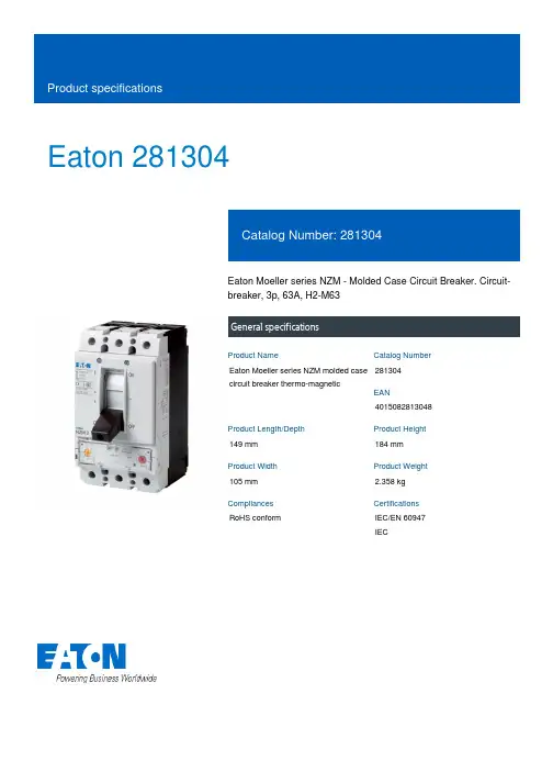
Eaton 281304Eaton Moeller series NZM - Molded Case Circuit Breaker. Circuit-breaker, 3p, 63A, H2-M63General specificationsEaton Moeller series NZM molded case circuit breaker thermo-magnetic2813044015082813048149 mm 184 mm 105 mm 2.358 kg RoHS conformIEC/EN 60947 IECProduct NameCatalog NumberEANProduct Length/Depth Product Height Product Width Product Weight Compliances Certifications690 V - 690 V 1000 V6000 V8000 V55 A (400 V AC-3) 1.9 kA1.9 kA63 A504 A882 A50 A63 A504 A882 A150 kA130 kA130 kA 6000 V8000 V55 A (400 V AC-3) 1.9 kA1.9 kA63 A504 A882 A50 A63 A504 A882 A150 kA130 kA130 kA37.5 kAVoltage ratingRated insulation voltage (Ui)Rated impulse withstand voltage (Uimp) at auxiliary contacts Rated impulse withstand voltage (Uimp) at main contacts Rated operational currentRated short-time withstand current (t = 0.3 s)Rated short-time withstand current (t = 1 s)Amperage RatingInstantaneous current setting (Ii) - minInstantaneous current setting (Ii) - maxOverload current setting (Ir) - minOverload current setting (Ir) - maxShort-circuit release non-delayed setting - minShort-circuit release non-delayed setting - maxRated short-circuit breaking capacity Ics (IEC/EN 60947) at 230 V, 50/60 HzRated short-circuit breaking capacity Ics (IEC/EN 60947) at 400/415 V, 50/60 HzRated short-circuit breaking capacity Ics (IEC/EN 60947) at 440 V, 50/60 Hz Rated impulse withstand voltage (Uimp) at auxiliary contacts Rated impulse withstand voltage (Uimp) at main contacts Rated operational currentRated short-time withstand current (t = 0.3 s)Rated short-time withstand current (t = 1 s)Amperage RatingInstantaneous current setting (Ii) - minInstantaneous current setting (Ii) - maxOverload current setting (Ir) - minOverload current setting (Ir) - maxShort-circuit release non-delayed setting - minShort-circuit release non-delayed setting - maxRated short-circuit breaking capacity Ics (IEC/EN 60947) at 230 V, 50/60 HzRated short-circuit breaking capacity Ics (IEC/EN 60947) at 400/415 V, 50/60 HzRated short-circuit breaking capacity Ics (IEC/EN 60947) at 440 V, 50/60 HzRated short-circuit breaking capacity Ics (IEC/EN 60947) at 525 V, 50/60 HzRated short-circuit breaking capacity Ics (IEC/EN 60947) at 69037.5 kA5 kA330 kA330 kA286 kA105 kA40 kA18.5 kW30 kW< 10 msScrew connection300 V AC (between the auxiliary contacts)500 V AC (between auxiliary contacts and main contacts) 120Rocker leverA (IEC/EN 60947-2)III35 kA330 kA330 kA286 kA105 kA40 kA18.5 kW30 kW< 10 msScrew connection300 V AC (between the auxiliary contacts)500 V AC (between auxiliary contacts and main contacts) 120Rocker leverA (IEC/EN 60947-2)III35000 operations at 690 V AC-36500 operations at 415 V AC-37500 operations at 690 V AC-110000 operations at 400 V AC-1Rated short-circuit breaking capacity Ics (IEC/EN 60947) at 525 V, 50/60 HzRated short-circuit breaking capacity Ics (IEC/EN 60947) at 690 V, 50/60 HzRated short-circuit making capacity Icm at 240 V, 50/60 Hz Rated short-circuit making capacity Icm at 400/415 V, 50/60 Hz Rated short-circuit making capacity Icm at 440 V, 50/60 Hz Rated short-circuit making capacity Icm at 525 V, 50/60 Hz Rated short-circuit making capacity Icm at 690 V, 50/60 Hz Rated operating power at AC-3, 230 VRated operating power at AC-3, 400 VShort-circuit total breaktimeElectrical connection type of main circuitIsolationNumber of operations per hour - maxHandle typeUtilization categoryOvervoltage categoryPollution degreeLifespan, electrical V, 50/60 HzRated short-circuit making capacity Icm at 240 V, 50/60 Hz Rated short-circuit making capacity Icm at 400/415 V, 50/60 Hz Rated short-circuit making capacity Icm at 440 V, 50/60 Hz Rated short-circuit making capacity Icm at 525 V, 50/60 Hz Rated short-circuit making capacity Icm at 690 V, 50/60 Hz Rated operating power at AC-3, 230 VRated operating power at AC-3, 400 VShort-circuit total breaktimeElectrical connection type of main circuitIsolationNumber of operations per hour - maxHandle typeUtilization categoryOvervoltage categoryPollution degreeLifespan, electrical5000 operations at 690 V AC-3 6500 operations at 415 V AC-3 7500 operations at 690 V AC-1 10000 operations at 400 V AC-1 6500 operations at 400 V AC-3 10000 operations at 415 V AC-1As required6500 operations at 400 V AC-3 10000 operations at 415 V AC-1As requiredBuilt-in device fixed built-in technique FixedIP20IP20 (basic degree of protection, in the operating controls area)IP40 (with insulating surround) IP66 (with door coupling rotary handle)IP10 (tunnel terminal)IP00 (terminations, phase isolator and strip terminal)Finger and back-of-hand proof to VDE 0106 part 10020 g (half-sinusoidal shock 20 ms)Thermomagnetic Damp heat, constant, to IEC 60068-2-78 Damp heat, cyclic, to IEC 60068-2-3020000 operationseaton-digital-nzm-brochure-br013003en-en-us.pdfeaton-feerum-the-whole-grain-solution-success-story-en-us.pdf eaton-digital-nzm-catalog-ca013003en-en-us.pdf Direction of incoming supply Direction of incoming supply Mounting MethodDegree of protection Degree of protection (IP), front side Degree of protection (terminations)Protection against direct contactShock resistanceSwitch off technique Climatic proofingLifespan, mechanical BrochuresCatalogsCharacteristic curveEaton Corporation plc Eaton House30 Pembroke Road Dublin 4, Ireland © 2023 Eaton. All Rights Reserved. Eaton is a registered trademark.All other trademarks areproperty of their respectiveowners./socialmediaeaton-circuit-breaker-let-through-current-nzm-mccb-characteristic-curve-005.epseaton-circuit-breaker-nzm-mccb-characteristic-curve-052.epseaton-circuit-breaker-characteristic-power-defense-mccb-characteristic-curve-037.eps eaton-circuit-breaker-switch-nzm-mccb-dimensions-017.eps eaton-circuit-breaker-nzm-mccb-dimensions-019.eps eaton-general-ie-ready-dilm-contactor-standards.eps MH2-M63il01206006z2015_11.pdf Introduction of the new digital circuit breaker NZM The new digital NZM Range DA-CS-nzm2_3p DA-CD-nzm2_3p eaton-nzm-technical-information-sheet eaton-manual-motor-starters-starter-nzm-mccb-wiring-diagram.eps eaton-manual-motor-starters-starter-msc-r-reversing-starter-wiring-diagram.epsDrawingseCAD modelInstallation instructions Installation videosmCAD model Technical data sheetsWiring diagrams。

MAX33251EELC+General DescriptionThe MAX33250E and MAX33251E are isolated2Tx/2Rx and1Tx/1Rx RS-232transceivers,respectively,with a galvanic isolation of600V RMS(60sec)between the logic UART side and field side.The isolation barrier protects the logic UART side from electrical transient strikes from the field side.It also breaks ground loops and large dif-ferences in ground potentials between the two sides that can potentially corrupt the receiving and sending of data. The MAX33250E and MAX33251E conform to the EIA/ TIA-232E standard and operate at data rates up to1Mbps. The isolated RS-232transceivers have integrated charge pumps and an inverter to eliminate the need for a high positive and negative voltage supply.Both devices also have integrated charge pump and inverter capacitors to help further reduce PCB space.The supply pin V CCA on the UART logic side operates from a dual voltage sup-ply from+3V to+5.5V.V CCB also operates from+3V to +5.5V,simplifying power requirements and enabling lev-el translation between the two voltages.The transmitters and receivers on the field side of these devices are rated for±15kV of ESD HBM protection,suitable for applications where RS-232 cables are frequently worked on.Both are available in a12-pin,6mm x6mm LGA package and operate over the -40ºC to +85ºC temperature range.Applications●Diagnostics Equipment●POS Systems●Industrial Equipment●GPS Equipment●Communication Systems●Medical Equipment Benefits and Features●High Integration Saves Space and Simplifies Designs•Integrated Charge Pumps and Inverter Eliminates Extra Power Supplies•Four Internal Capacitors Saves PCB Space•Integrated Isolator Saves Up to 63% Versus a Discrete Solution●Integrated Protection for Robust Communications•600V RMS Withstand Isolation Voltage for 60 Seconds (V ISO)•200V RMS Working Voltage for >50 years (V IOWM)•Integrated ±15kV ESD Human Body Model (HBM) Ordering Information appears at end of data sheet.Click here for production status of specific part numbers.MAX33250E/ MAX33251E 600V Isolated 2Tx/2Rx and 1Tx/1Rx RS-232Transceiver with ±15kV ESDand Integrated CapacitorsEVALUATION KIT AVAILABLE19-100400, Rev 1; 11/18Absolute Maximum RatingsV CCA to GNDA.........................................................-0.3V to +6V V CCB to GNDB.........................................................-0.3V to +6V T_IN to GNDA..........................................................-0.3V to +6V T_OUT to GNDB...............................................................±13.2V R_IN to GNDB......................................................................±25V R_OUT to GNDA......................................................-0.3V to +6V Short-Circuit Duration (T_OUT to GNDB)..................Continuous Short-Circuit Duration (R_OUT to GNDA)..................ContinuousSide A (V CCA , T1IN, T2IN, R1OUT, R2OUT) to GNDA ESD±2kV Side B (V CCB ) to GNDB ESD...............................................±2kV Side B (T1OUT, T2OUT, R1IN, R2IN) to GNDB ESD HBM±15kV Continuous Power Dissipation (Single Layer Board)(T A =+70°C,derate 10mW/°C above +70°C.)...........................510mW Continuous Power Dissipation (Multilayer Board)(T A =+70°C,derate 10mW/°C above +70°C.)...........................700mW Operating Temperature Range.............................-40°C to +85°CStresses beyond those listed under “Absolute Maximum Ratings” may cause permanent damage to the device. These are stress ratings only, and functional operation of the device at these or any other conditions beyond those indicated in the operational sections of the specifications is not implied. Exposure to absolute maximum rating conditions for extended periods may affect device reliability.Package InformationLGA-12For the latest package outline information and land patterns (footprints), go to /packages .Note that a “+”, “#”, or “-” in the package code indicates RoHS status only. Package drawings may show a different suffix character, but the drawing pertains to the package regardless of RoHS status.Package thermal resistances were obtained using the method described in JEDEC specification JESD51-7, using a four-layer board. For detailed information on package thermal considerations, refer to /thermal-tutorial .MAX33250E/MAX33251E600V Isolated 2Tx/2Rx and 1Tx/1Rx RS-232Transceiver with ±15kV ESD and Integrated CapacitorsElectrical Characteristics(V CCA -V GNDA =3.0V to 5.5V,V CCB -V GNDB =3.0V to 5.5V,T A =T MIN to T MAX ,unless otherwise noted.Typical values are at V CCA -V GNDA =3.3V,V CCB -V GNDB =3.3V,V GNDA =V GNDB ,and T A =+25°C.(Note 1),Limits are 100%tested at T A =+25°C.Limits over the operating temperature range and relevant supply voltage range are guaranteed by design and characterization.Specifications marked "GBD" are guaranteed by design and not production tested.)PARAMETER SYMBOLCONDITIONSMINTYPMAXUNITSPOWER Supply VoltageV CCA , V CCB3.05.5VSupply CurrentI CCAV CCA = 5V, R_IN and T_IN idle 12mA V CCA = 3.3V, R_IN and T_IN idle 10I CCBV CCB = 5V, R_IN and T_IN idle, no load 12V CCB = 3.3V, R_IN and T_IN idle, no load10Undervoltage-Lockout ThresholdV UVLO V CCA - V GNDA (Note 2) 2.0V Undervoltage-Lockout HysteresisV UVLOHYSV CCA - V GNDA (Note 2)0.1V INPUT INTERFACE (T_IN, R_IN)Input Low VoltageV ILT_IN relative to GNDA0.8VR_IN relative to GNDB, T A = 25ºC,V CC = 3.3V0.6R_IN relative to GNDB, T A = 25ºC,V CC = 5V0.8Input High VoltageV IHT_IN relative to GNDA0.7 x V CCA VR_IN relative to GNDB, V CCB = 3.3V and 5V, T A = 25°C 2.4Transmitter Input Hysteresis (T_IN)0.5V Receiver Input Hysteresis (R_IN)0.5V Transmitter Input Leakage(T_IN)±1μA Input Resistance (R_IN)T A = 25ºC357kΩRECEIVER OUTPUT INTERFACE (R_OUT)Output Low Voltage V OL R_OUT relative to GNDA,sink current = 4mA 0.8V Output High Voltage V OHR_OUT relative to GNDA,source current = 4mAV CCA -0.4V Output Short-Circuit Current±110mATRANSMITTER OUTPUT (T_OUT)Output Voltage SwingT_OUT loaded with 3kΩ to GNDB±5VMAX33250E/MAX33251E600V Isolated 2Tx/2Rx and 1Tx/1Rx RS-232Transceiver with ±15kV ESD and Integrated CapacitorsElectrical Characteristics (continued)(V CCA -V GNDA =3.0V to 5.5V,V CCB -V GNDB =3.0V to 5.5V,T A =T MIN to T MAX ,unless otherwise noted.Typical values are at V CCA -V GNDA =3.3V,V CCB -V GNDB =3.3V,V GNDA =V GNDB ,and T A =+25°C.(Note 1),Limits are 100%tested at T A =+25°C.Limits over the operating temperature range and relevant supply voltage range are guaranteed by design and characterization.Specifications marked "GBD" are guaranteed by design and not production tested.)PARAMETER SYMBOLCONDITIONSMIN TYP MAXUNITS Output Resistance V CCB = 0V,transmitters = ±2V30010MΩOutput Short-Circuit Current±70mA Output Leakage CurrentV CCB = 0V, V OUT =±12V±25μAESD AND ISOLATION PROTECTIONESD for R_IN, T_OUTIEC 61000-4-2 Air Discharge±12kVIEC 61000-4-2 Contact Discharge ±6ESD Human Body Model JEDEC JS-001-2014±15Isolation Voltage V ISO t = 60s (Note 3)600V RMS Working Isolation VoltageV IOWM> 50 years (Note 3)200V RMS TIMING CHARACTERISTICS Maximum Data Rate V CCB = 5V, R L = 3kΩ, C L = 1000pF 1000kbps Receiver Propagation Delayt PHL , t PLH R_IN to R_OUT, C L = 150pF0.15μs Transmitter Skew | t PHL - t PLH |(Note 4)35ns Receiver Skew | t PHL - t PLH |60ns Transition-Region Slew RateV CCA = V CCB = 3.3V, T A = +25C, R L =3k to 7k, C L = 150pF to 1000pF,measured from +3V to -3V or -3V to +3V24150V/μsNote 1:All units are production tested at T A =25°C.Specifications over temperature are guaranteed by design.All voltages of side Aare referenced to GNDA. All voltages of side B are referenced to GNDB.Note 2:The undervoltage lockout threshold and hysteresis guarantee that the outputs are in a known state when the supply voltagedips.Note 3:The isolation is guaranteed by design and not production tested.Note 4:Transmitter skew is measured at the transmitter zero cross points.MAX33250E/MAX33251E600V Isolated 2Tx/2Rx and 1Tx/1Rx RS-232Transceiver with ±15kV ESD and Integrated CapacitorsTypical Operating Characteristics (V DD= 5V, V L= 3.3V, R L= 60Ω, C L= 15pF, T A= +25°C, unless otherwise noted.)MAX33250E/MAX33251E600V Isolated 2Tx/2Rx and 1Tx/1Rx RS-232Transceiver with ±15kV ESDand Integrated CapacitorsTypical Operating Characteristics (continued) (V DD= 5V, V L= 3.3V, R L= 60Ω, C L= 15pF, T A= +25°C, unless otherwise noted.)MAX33250E/MAX33251E600V Isolated 2Tx/2Rx and 1Tx/1Rx RS-232Transceiver with ±15kV ESDand Integrated CapacitorsMAX33250E/MAX33251E600V Isolated 2Tx/2Rx and 1Tx/1Rx RS-232Transceiver with ±15kV ESDand Integrated Capacitors Pin ConfigurationsPin DescriptionPINNAME FUNCTIONMAX33250EMAX33251E11V CCA Supply Voltage of Logic Side A. Bypass V CCA with a 0.1μF ceramic capacitor to GNDA 22T1IN TTL/CMOS Transmitter Input 13---T2IN TTL/CMOS Transmitter Input 244R1OUT TTL/CMOS Receiver Output 15---R2OUT TTL/CMOS Receiver Output 266GNDA Ground for Logic Side A 77GNDB Ground for Field Side B 8---R2IN RS-232 Receiver Input 299R1IN RS-232 Receiver Input 110---T2OUT RS-232 Transmitter Output 21111T1OUT RS-232 Transmitter Output 11212V CCBSupply Voltage of Logic Side B. Bypass V CCB with a 0.1μF ceramic capacitor to GNDBMAX33250E/MAX33251E600V Isolated 2Tx/2Rx and 1Tx/1Rx RS-232Transceiver with ±15kV ESD and Integrated CapacitorsMAX33250E/MAX33251E600V Isolated 2Tx/2Rx and 1Tx/1Rx RS-232Transceiver with ±15kV ESDand Integrated Capacitors Detailed DescriptionThe MAX33250E and MAX33251E are1Mbps,600V RMS isolated RS-232transceivers.The MAX33250E has2 transmitters and2receivers(2Tx/2Rx),and the MAX33251E has1transmitter and1receiver(1Tx/1Rx).The isolation is provided by Maxim’s proprietary insulation material that can withstand600V RMS for60seconds.The MAX33250E and MAX33251E conform to the EIA/TIA-232standard and operates at data rates up to1Mbps over the temperature range of -40ºC to 85ºC.Digital IsolationThe MAX33250E and MAX33251E provide galvanic isolation and protection for digital signals from the local microcontroller’s logic UART port(primary side)to the field lines(secondary side).A capacitive design is utilized where the insulation material for the isolation barrier is rated for600V RMS withstand voltage(V ISO)for60seconds.The same material can also be exposed to a differential of200V RMS of working voltage(V IOWM)for more than50years,providing longevity for many different types of end equipment.The isolation barrier also breaks ground loops and level translation for two different systems where it could potentially create inadvertent or misinterpret data signals.Dual Charge Pump Voltage Converter and InverterBoth parts have internal RS-232power supplies that consist of a regulated dual charge pump that provides output voltages of+5.5V(doubling charge pump)and-5.5V(inverting charge pump),over the+3.0V to+5.5V range.Each charge pump is internally connected to a pair of flying capacitors and a pair of reservoir capacitors to generate the internal V+ and V- supplies, as shown in Typical Application Diagram.Startup and Undervoltage LockoutThe V CCA and V CCB supplies are both internally monitored for undervoltage conditions.Undervoltage events can occur during power-up,power-down,or during normal operation due to a dip in either power supply line.When an undervoltage event is detected on either of the supplies,all outputs on both sides are automatically controlled,regardless of the status of the inputs.Table 1. Output Control Truth TableINPUTS V CCA V CCB RxOUT TxOUT RxIN = 1Undervoltage Powered High---RxIN = 0Undervoltage Powered Follows V CCA---TxIN = 1Undervoltage Powered—LowTxIN = 0Undervoltage Powered—LowRxIN = 1Powered Undervoltage High---RxIN = 0Powered Undervoltage High---TxIN = 1Powered Undervoltage—*LowTxIN = 0Powered Undervoltage—*Low*TxOUT will be out of compliance with the RS-232 specification as V CCB falls below 2.9V.Transceiver with ±15kV ESDand Integrated CapacitorsRS-232 TransmittersThe transmitters are inverting level translators that convert CMOS-logic levels from the UART or equivalent output port to+5V EIA/TIA-232levels.The two devices guarantee1Mbps with worst-case loads of3kΩin parallel with1000pF, providing compatibility with PC-to-PC communication software.Transmitters can be paralleled to drive multiple receivers. RS-232 ReceiversThe receivers convert RS-232signals to CMOS-logic output levels to the UART or equivalent input port.The devices feature inverting outputs that always remain active.Power Supply DecouplingTo reduce ripple and the chance of introducing data errors,bypass V CCA and V CCB with0.1μF ceramic capacitors to GNDA and GNDB, respectively. Place the bypass capacitors as close to the power-supply input pins as possible.Insulation and Safety CharacteristicsPARAMETERSYMBOL CONDITIONSVALUE UNIT IEC INSULATION AND SAFETY RELATED FOR SPECIFICATIONSExternal Tracking (Creepage)CPG IEC 60664-1 4.4mm External Air Gap (Clearance)CLRIEC 60664-1 4.4mm Minimum Internal Gap Insulation Thickness 0.0026mm Tracking Resistance(Comparative Tracking Index)CTI IEC 112/VDE 030 Part 1175V Insulation Resistance Across Barrier R ISO 1GΩCapacitance Across Isolation BarrierC IOf = 1MHz12pFVDE IEC INSULATION CHARACTERISTICS Surge Isolation VoltageV IOSM IEC 60747-17,section 5.3.1.6and 5.4.6for basic insulation1kV PEAK Repetitive Peak Isolation Voltage V IORM IEC 60747-17, section 5.3.1.3282kV PEAK Rated Transient Isolation Voltage V IOTM IEC 60747-17, section 5.3.1.4850kV PEAK Safety Limiting Temperature T S IEC 60747-17, section 7.2.1150°C Safety Limiting SideAPowerDissipation P SAIEC 60747-17, section 7.2.10.75WSafety Limiting Side B PowerDissipationP SB IEC 60747-17, section 7.2.10.75W Apparent Charge Method q pdIEC 60747-17, section 7.4 method a and b 5pC Overvoltage Category IEC 60664-1, single or three phase 50V DC or AC I,II —Overvoltage Category IEC 60664-1,single or three phase 100V DC or AC I —Climatic Category 40/125/21—Pollution DegreeDIN VDE 01102—Transceiver with ±15kV ESD and Integrated CapacitorsTransceiver with ±15kV ESDand Integrated Capacitors Typical Application CircuitOrdering InformationPART NUMBER TEMPERATURERANGE CHANNEL-CONFIGURATION DATA RATE PIN-PACKAGE MAX33250EELC+-40°C to +85°C 2 Transmitters, 2 Receivers 1Mbps 12 (6mm x 6mm) LGA MAX33251EELC+-40°C to +85°C1 Transmitter, 1 Receiver1Mbps12 (6mm x 6mm) LGA+Denotes a lead(Pb)-free/RoHS-compliant package.T = Tape-and-reel.Transceiver with ±15kV ESD and Integrated CapacitorsRevision HistoryREVISION NUMBERREVISION DATE DESCRIPTIONPAGES CHANGED09/18Initial release—111/18Updated Ordering Information13For pricing, delivery, and ordering information, please visit Maxim Integrated’s online storefront at https:///en/storefront/storefront.html.Maxim Integrated cannot assume responsibility for use of any circuitry other than circuitry entirely embodied in a Maxim Integrated product. No circuit patentlicenses are implied. Maxim Integrated reserves the right to change the circuitry and specifications without notice at any time. The parametric values (min and max limits) shown in the Electrical Characteristics table are guaranteed. Other parametric values quoted in this data sheet are provided for guidance.Transceiver with ±15kV ESD and Integrated CapacitorsMAX33251EELC+。
SURMOUNT TM Low, Medium and HighBarrier Silicon Schottky Diodes V5MA4E2502 SeriesFeatures•Extremely Low Parasitic Capitance andInductance•Surface Mountable in Microwave Circuits, NoWirebonds Required•Rugged HMIC Construction with PolyimideScratch Protection•Reliable, Multilayer Metalization with a DiffusionBarrier, 100% Stabilization Bake (300 °C,16 hours)•Lower Susceptibility to ESD DamageDescription and ApplicationsThe MA4E2502 SurMount TM Series Diodes are Silicon Low, Medium, and High Barrier Schottky Devices fabricated with the patented Heterolithic Microwave Integrated Circuit (HMIC) process. HMIC circuits consist of Silicon pedestals which form diodes or via conductors embedded in a glass dielectric, which acts as the low dispersion, microstrip transmission medium. The combination of silicon and glass allows HMIC devices to have excellent loss and power dissipation characteristics in a low profile, reliable device.The Surmount Schottky devices are excellent choices for circuits requiring the small parasitics of a beam lead device coupled with the superior mechanical performance of a chip. The SurMount structure employs very low resistance silicon vias to connect the Schottky contacts to the metalized mounting pads on the bottom surface of the chip. These devices are reliable, repeatable, and a lower cost performance solution to conventional devices. They have lower susceptibility to electrostatic discharge than conventional beam lead Schottky diodes.The multi-layer metalization employed in the fabrication of the Surmount Schottky junctions includes a platinum diffusion barrier, which permits all devices to be subjected to a 16-hour non-operating stabilization bake at 300 °C.The “ 0502 ” outline allows for Surface Mount placement and multi-functional polarity orientations. Case Style 1246The MA4E2502 Family of SurMount Schottky diodes are recommended for use in microwave circuits through Ku band frequencies for lower power applications such as mixers, sub-harmonic mixers, detectors and limiters. The HMIC construction facilitates the direct replacement of more fragile beam lead diodes with the corresponding Surmount diode, which can be connected to a hard or soft substrate circuit with solder.DimInches MillimetersMin. Max. Min. Max.A 0.0445 0.0465 1.130 1.180B 0.0169 0.0189 0.430 0.480C 0.0040 0.0080 0.102 0.203D Sq. 0.0128 0.325E 0.0128 0.0148 0.325 0.3750.0148 0.375SURMOUNT TM Low, Medium and High Barrier Silicon Schottky DiodesV5MA4E2502 SeriesElectrical Specifications @ 25 °CHandlingAll semiconductor chips should be handled with care to avoid damage or contamination from perspiration and skin oils. The use of plastic tipped tweezers or vacuum pickups is strongly recommended for individual components. The top surface of the die has a protective polyimide coating to minimize damage.The rugged construction of these SurMount devices allows the use of standard handling and die attach techniques. It is important to note that industry standard electrostatic discharge (ESD) control is required at all times, due to the sensitive nature of Schottky junctions.Bulk handling should insure that abrasion and mechanical shock are minimized.Die BondingDie attach for these devices is made simple through the use of surface mount die attach technology. Mounting pads are conveniently located on the bottom surface of these devices, and are opposite the active junction. The devices are well suited for high temperature solder attachment onto hard substrates. 80Au/20Sn and Sn63/Pb37 solders are acceptable for usage. Die attach with Electrically Conductive Silver Epoxy is Not Recommended.For Hard substrates, we recommend utilizing a vacuum tip and force of 60 to 100 grams applied uniformly to the top surface of the device, using a hot gas bonder with equal heat applied across the bottom mounting pads of the device. When soldering to soft substrates, it is recommended to use a lead-tin interface at the circuit board mounting pads. Position the die so that its mounting pads are aligned with the circuit board mounting pads. Reflow the solder paste by applying Equal heat to the circuit at both die-mounting pads. The solder joint must Not be made one at a time, creating un-equal heat flow and thermal stress. Solder reflow should Not be performed by causing heat to flow through the top surface of the die. Since the HMIC glass is transparent, the edges of the mounting pads can be visually inspected through the die after die attach is completed.Absolute Maximum Ratings @ 25 °C (Unless Otherwise Noted) 11.Operation of this device above any one of these parameters may cause permanent damage. Parameter Absolute Maximum Operating Temperature -40 °C to +125 °C Storage Temperature -40 °C to +150 °CJunction Temperature +175 °C Forward Current 20 mA Reverse Voltage 5 V RF C.W. Incident Power + 20 dBm RF & DC Dissipated Power50 mWRt is the dynamic slope resistance whereRt = Rs + Rj, where Rj = 26 / Idc (Idc is in mA)Model Number TypeRecommended Frequency Range Vf @ 1 mA ( mV ) Vb @ 10 uA( V )Ct @ 0V ( pF ) Rt Slope Resistance ( Vf1 - Vf2 )/(10.5mA-9.5mA )( Ω )MA4E2502L Low Barrier DC - 18 GHz 330 Max 300 Typ3 Min 5 Typ 0.12 Max 0.10 Typ 16 Typ 20 MaxMA4E2502M Medium Barrier DC - 18 GHz 470 Max 420 Typ 3 Min 5 Typ 0.12 Max 0.10 Typ 12 Typ 18 Max MA4E2502HHigh BarrierDC - 18 GHz700 Max 650 Typ3 Min 5 Typ0.12 Max 0.10 Typ11 Typ 15 MaxSURMOUNT TM Low, Medium and High Barrier Silicon Schottky DiodesV5MA4E2502 SeriesMA4E2502L Low Barrier SPICE PARAMETERSIs (nA) Rs ( Ω ) N Cj0 ( pF ) M Ik (mA) Cjpar (pF) Vj (V) FCBV (V) IBV (mA) 5 E-19.61.201.0 E-020.5109.0 E-28.0 E-20.5 5.01.0 E-2Is (nA) Rs ( Ω ) N Cj0 ( pF ) M Ik (mA) Cjpar (pF) Vj (V) FCBV (V) IBV (mA) 2612.81.201.0 E-20.5149.0 E-28.0 E-20.5 5.01.0 E-2MA4E2502M Medium Barrier SPICE PARAMETERSIs(nA) Rs ( Ω ) N Cj0 ( pF ) M Ik (mA) Cjpar (pF) Vj (V) FCBV (V) IBV (mA) 5.7 E-16.51.201.0 E-020.549.0 E-28.0 E-20.5 5.01.0 E-2MA4E2502H High Barrier SPICE PARAMETERSSURMOUNT TM Low, Medium and High Barrier Silicon Schottky DiodesV5MA4E2502 SeriesOrdering InformationPart Number Package MA4E2502L-1246W Wafer on Frame MA4E2502L-1246 Die in Carrier MA4E2502L-1246T Tape/Reel MA4E2502M-1246W Wafer on Frame MA4E2502M-1246Die in Carrier MA4E2502M-1246T Tape/Reel MA4E2502H-1246W Wafer on Frame MA4E2502H-1246 Die in Carrier MA4E2502H-1246TTape/ReelMA4E2502 Diode SchematicLsRs RjCtSchematic ValuesModel NumberLs (nH) Rs ( Ω ) Rj ( Ω ) Ct (pF) MA4E2502L 0.8 12.8 26 / Idc (mA) 0.10 MA4E2502M 0.8 9.6 26 / Idc (mA) 0.10 MA4E2502H0.86.526 / Idc (mA)0.10。
Eaton 278442Eaton Moeller® series ZB Motorschutzrelais, ZB32, Ir= 0,1 - 0,16A, 1 S, 1 Ö, Direktmontage, IP20Allgemeine spezifikationEaton Moeller® series ZB Thermaloverload relay278442401508278442396 mm67 mm45 mm0.141 kgUL File No.: E29184CSA Class No.: 3211-03CSA-C22.2 No. 60947-4-1-14 IEC/EN 60947VDE 0660IEC/EN 60947-4-1ULUL Category Control No.: NKCR CSA File No.: 012528CECSAUL 60947-4-1Überlastrelais thermisch ZB32-0,16Produktname KatalognummerEANProdukt Länge/Tiefe Produkthöhe Produktbreite Produktgewicht Zertifikat(e)ProdukttypModellcodePhasenausfallempfindlichkeit (gemäß IEC/EN 60947, VDE 0660 Teil 102)Reset-Taste Hand/Auto Freiauslösung Test/Aus-Taste-25 °C55 °C25 °C40 °C CLASS 10 A Feuchte Wärme, konstant, nach IEC 60068-2-78 Feuchte Wärme, zyklisch, nach IEC 60068-2-30IP20ZB32Direct attachment Direktanbau0.1 A0.16 AIII3Finger- und handrückensicher, Berührungsschutz bei senkrechter Betätigung von vorne (EN 50274)MerkmaleUmgebungsbetriebstemperatur – min Umgebungsbetriebstemperatur – max Umgebungsbetriebstemperatur (gekapselt) – min Umgebungsbetriebstemperatur (gekapselt) – max Klasse KlimafestigkeitSchutzart Rahmengr.Montageart Überlastauslösestromeinstellung - min Überlastauslösestromeinstellung - max Überspannungskategorie Verschmutzungsgrad Produktkategorie SchutzZubehörMotorschutzrelais ZB bis 150 A6000 V AC4000 V (Hilfs- und Steuerkreise)10 g, Mechanisch, Sinusförmig, Schockdauer 10 ms Nebenstromkreise, (UL/CSA)≤ 0,25 %/K, Restfehler für T > 40° Kontinuierlich 2 x (0,75 - 2,5) mm², Steuerstromleitungen2 x (1 - 4) mm², Hauptleiter1 x (1 - 4) mm², Hauptleiter1 x (0,75 - 2,5) mm², Steuerstromleitungen1 x (0,75 - 4) mm², Steuerstromleitungen2 x (0,75 - 4) mm², Steuerstromleitungen1 x (1 - 6) mm², Hauptleiter2 x (1 - 6) mm², Hauptleiter2 x (18 - 14), Steuerstromleitungen18 - 8, Hauptleiter10 mm8 mmM3,5, Anschlussschraube, HilfsleiterM4, Anschlussschraube2, Anschlussschraube, Pozidriv-Schraubendreher1 x 6 mm, Anschlussschraube, Schlitzschraubendreher1,2 Nm, Schraubklemmen, Steuerstromleitungen1.8 Nm, Schraubklemmen, Hauptleiter6 A 1.5 A 1.5 A 0.9 A 100 kA, Sicherung, SCCR (UL/CSA)1 A, Klasse J/CC, max. Sicherung, SCCR (UL/CSA)0,5 A gG/gL, Sicherung, Zuordnungsart "2"Max. 6 A gG/gL, Sicherung, Ohne Verschweißen, Hilfs- und Steuerkreise25 A gG/gL, Sicherung, Zuordnungsart "1"Bemessungsstoßspannungsfestigkeit (Uimp)Schockfestigkeit Geeignet für Temperaturkompensation Anschlusskapazität (freindrähtig mit Aderendhülse) Anschlusskapazität (fest)Anschlusskapazität (ein-/mehrdrähtig AWG) Abisolierlänge (Hauptleiter)Abisolierlänge (Hilfsleiter)Schr-GröSchraubendrehergrößeAnzugsdrehmomentKonventioneller thermischer Strom lth der Hilfskontakte (1-polig, offen)Bemessungsbetriebsstrom (le) bei AC-15, 120 V Bemessungsbetriebsstrom (le) bei AC-15, 220 V, 230 V, 240 V Bemessungsbetriebsstrom (le) bei AC-15, 380 V, 400 V, 415 V Bemessungskurzschlussstrom (hoher Fehlerstrom bei 600 V) Bemessungsdaten Kurzschlussschutz0.4 A0.2 A0.9 A0.75 A690 V440 V, Zwischen Hilfskontakten und Hauptkontakten, Entspricht EN 61140440 V AC, zwischen den Hauptstrombahnen, Entspricht EN 61140240 V AC, Zwischen Hilfskontakten, Entspricht EN 61140B300 bei gegenüberliegender Polarität, AC-betätigt (UL/CSA) B600 bei gegenüberliegender Polarität, AC-betätigt (UL/CSA) R300, DC-betätigt (UL/CSA)600 VAC600 VAC 011115.4 W0 W1.8 W0.16 A0 WAnforderungen der Produktnorm sind erfüllt.Anforderungen der Produktnorm sind erfüllt.Anforderungen der Produktnorm sind erfüllt.Anforderungen der Produktnorm sind erfüllt.Anforderungen der Produktnorm sind erfüllt.Unzutreffend, da die gesamten Schaltgeräte überprüft werdenBemessungsbetriebsstrom (le) bei DC-13, 110 VBemessungsbetriebsstrom (le) bei DC-13, 220 V, 230 V Bemess.betriebsstrom (le) bei DC-13, 24 V Bemessungsbetriebsstrom (le) bei DC-13, 60 V Bemessungsbetriebsspannung (Ue) - maxSichere TrngSchaltvermögen (Hilfskontakte, Steuerzyklus) Nennspannung - maxNennspannung - max Anzahl der Hilfskontakte (Wechsler)Anzahl der Hilfskontakte (Öffner)Anzahl Hilfskontakte (Schließer)Anzahl der Kontakte (Öffner)Anzahl der Kontakte (Schließer)Geräteverlustleistung, stromabhängig pvid Verlustleistungskapazität PdissVerlustleistung pro Pol, stromabhängig, Pvid Bemessungsbetriebsstrom zur Verlustleistungsangabe (In) Statische Verlustleistung, stromunabhängig PVS10.2.2 Korrosionsbeständigkeit10.2.3.1 Wärmebeständigkeit von Umhüllung10.2.3.2 Widerstandsfähigkeit Isolierstoffe gewöhnliche Wärme 10.2.3.3 Widerst. Isolierstoffe abnorm. Wärme/Feuer durch int. elektr. Auswirk.10.2.4 Beständigkeit gegen UV-Strahlung10.2.5 Hebenmüssen.Unzutreffend, da die gesamten Schaltgeräte überprüft werdenmüssen.Anforderungen der Produktnorm sind erfüllt.Unzutreffend, da die gesamten Schaltgeräte überprüft werden müssen.Anforderungen der Produktnorm sind erfüllt.Unzutreffend, da die gesamten Schaltgeräte überprüft werden müssen.Unzutreffend, da die gesamten Schaltgeräte überprüft werden müssen.Liegt in der Verantwortung des Schaltanlagenbauers.Liegt in der Verantwortung des Schaltanlagenbauers.Liegt in der Verantwortung des Schaltanlagenbauers.Liegt in der Verantwortung des Schaltanlagenbauers.Liegt in der Verantwortung des Schaltanlagenbauers.Die Erwärmungsberechnung liegt in der Verantwortung des Schaltanlagenbauers. Eaton stellt Verlustleistungsdaten der Geräte bereit.Liegt in der Verantwortung des Schaltanlagenbauers. Die Spezifikationen für die Schaltgeräte müssen beachtet werden.Liegt in der Verantwortung des Schaltanlagenbauers. Die Spezifikationen für die Schaltgeräte müssen beachtet werden.Das Gerät erfüllt die Anforderungen, wenn die Informationen in eaton-motor-protective-relay-zb12-zb32-overload-monitoring-exe-manual-mn03407004z-de-de-en-us.pdfDA-DC-00004853.pdfDA-DC-00004843.pdfETN.ZB32-0,16IL03407015ZIL03407195ZSortimentskatalog Motoren schalten und schützenDA-CD-zb32DA-CS-zb3210.2.6 Schlagprüfung10.2.7 Beschriftungen10.3 Schutzart von Baugruppen10.4 Luft- und Kriechstrecken10.5 Schutz gegen elektrischen Schlag10.6 Einbau von Betriebsmitteln10.7 Innere Stromkreise und Verbindungen10.8 Anschlüsse für von außen eingeführte Leiter 10.9.2 Betriebsfrequente Spannungsfestigkeit 10.9.3 Stoßspannungsfestigkeit10.9.4 Prüfung von Umhüllungen aus Isolierstoff 10.10 Erwärmung10.11 Kurzschlussfestigkeit10.12 Elektromagnetische Verträglichkeit10.13 Mechanische Funktion Benutzerhandbücher Declarations of conformity eCAD model Installationsanleitung KatalogemCAD modelEaton Konzern plc Eaton-Haus30 Pembroke-Straße Dublin 4, Irland © 2023 Eaton. Alle Rechte vorbehalten. Eaton ist eine eingetrageneMarke.Alle anderen Warenzeichen sindEigentum ihrer jeweiligenBesitzer./socialmediader Montageanweisung (IL) beachtet werden.。
SURMOUNT TM Low Barrier Tee“0301” Footprint Silicon Schottky Diodes Series V1MA4E2513-1289Features•Extremely Low Parasitic Capitance andInductance•Extremely Small “0301” (1000 x 300um) Footprint•Surface Mountable in Microwave Circuits, NoWirebonds Required•Rugged HMIC Construction with PolyimideScratch Protection•Reliable, Multilayer Metalization with a Diffusion•Barrier, 100% Stabilization Bake (300°C, 16 hours)•Lower Susceptibility to ESD DamageDescription and ApplicationsThe MA4E2513L-1289 SurMount™ Diodes are Silicon Low Barrier Schottky Devices fabricated with the patented Heterolithic Microwave Integrated Circuit (HMIC) process. HMIC circuits consist of Silicon pedestals which form diodes or via conductors embedded in a glass dielectric, which acts as the low dispersion, microstrip transmission medium. The combination of silicon and glass allows HMIC devices to have excellent loss and power dissipation characteristics in a low profile, reliable device. The Surmount Schottky devices are excellent choices for circuits requiring the small parasitics of a beam lead device coupled with the superior mechanical performance of a chip. The SurMount structure employs very low resistance silicon vias to connect the Schottky contacts to the metalized mounting pads on the bottom surface of the chip. These devices are reliable, repeatable, and a lower cost performance solution to conventional devices. They have lower susceptibility to electrostatic discharge than conventional beam lead Schottky diodes.The multi-layer metalization employed in the fabrication of the Surmount Schottky junctions includes a platinum diffusion barrier, which permits all devices to be subjected to a 16-hour non-operating stabilization bake at 300°C.The extremely small “ 0301 ” outline allows for Surface Mount placement and multi-functional polarity orientations. Case Style 1289top, side and bottom viewsDimInches MillimetersMin. Max. Min. Max.A 0.038 0.040 0.975 1.025B 0.011 0.013 0.275 0.325C 0.004 0.008 0.102 0.203D 0.007 0.175E 0.007 0.009 0.175 0.2250.009 0.225The MA4E2513L-1289 SurMount Low Barrier Schottky diodes are recommended for use in microwave circuits through Ku band frequencies for lower power applications such as mixers, sub-harmonic mixers, detectors and limiters. The HMIC construction facilitates the direct replacement of more fragile beam lead diodes with the corresponding Surmount diode, which can be connected to a hard or soft substrate circuit with solder.Cathode 1 Common Anode 2SURMOUNT TM Low Barrier Tee“0301” Footprint Silicon Schottky DiodesSeries V1MA4E2513-1289Electrical Specifications @ 25 °C (per junction)HandlingAll semiconductor chips should be handled with care to avoid damage or contamination from perspiration and skin oils. The use of plastic tipped tweezers or vacuum pickups is strongly recommended for individual components. The top surface of the die has a protective polyimide coating to minimize damage.The rugged construction of these SurMount devices allows the use of standard handling and die attach techniques. It is important to note that industry standard electrostatic discharge (ESD) control is required at all times, due to the sensitive nature of Schottky junctions.Bulk handling should insure that abrasion and mechanical shock are minimized.Die BondingDie attach for these devices is made simple through the use of surface mount die attach technology. Mounting pads are conveniently located on the bottom surface of these devices, and are opposite the active junction. The devices are well suited for higher temperature solder attachment onto hard substrates. 80Au/20Sn and Sn63/Pb37 solders are acceptable for usage. Die attach with Electrically Conductive Silver Epoxy is Not Recommended.For Hard substrates, we recommend utilizing a vacuum tip and force of 60 to 100 grams applied uniformly to the top surface of the device, using a hot gas bonder with equal heat applied across the bottom mounting pads of the device. When soldering to soft substrates, it is recommended to use a lead-tin interface at the circuit board mounting pads. Position the die so that its mounting pads are aligned with the circuit board mounting pads. Reflow the solder paste by applying Equal heat to the circuit at both die-mounting pads. The solder joint must Not be made one at a time, creating un-equal heat flow and thermal stress. Solder reflow should Not be performed by causing heat to flow through the top surface of the die. Since the HMIC glass is transparent, the edges of the mounting pads can be visually inspected through the die after die attach is completed.Absolute Maximum Ratings @ 25 °C (Unless Otherwise Noted) 11.Operation of this device above any one of these parameters may cause permanent damage.Parameter Absolute Maximum Operating Temperature -40 °C to +150 °C Storage Temperature -40 °C to +150 °CJunction Temperature +175 °C Forward Current 20 mA Reverse Voltage 5 V RF C.W. Incident Power + 20 dBm RF & DC Dissipated Power50 mWRt is the dynamic slope resistance where Rt = Rs + Rj , where Rj =26 / Idc ( Idc is in mA) and Rs is the Ohmic Resistance.Model Number TypeRecommended Frequency Range Vf @ 1 mA ( mV ) Ct @ 0 V ( pF ) Rt Slope Resistance( Vf1 - Vf2 ) / (10.5mA-9.5mA )( Ω ) MA4E2513L-1289Low BarrierDC - 18 GHz330 Max 300 Typ0.12 Max 0.10 Typ10 Typ 14 MaxVb @ 10 uA(V)3 Min 5 TypSURMOUNT TM Low Barrier Tee“0301” Footprint Silicon Schottky DiodesSeries V1MA4E2513-1289MA4E2513L-1289 Low Barrier SPICE PARAMETERSIs (nA) Rs ( Ω ) N Cj0 ( pF ) M Ik (mA) Cpar (pF) Vj (V) FC BV (V) IBV (mA) 2612.81.201.0 E-20.5149.0 E-28.0 E-20.55.01.0 E-2Circuit Mounting Dimensions (Inches)Ordering InformationPart Number Package MA4E2513L-1289W Wafer on Frame MA4E2513L-1289 Die in Carrier MA4E2513L-1289TTape/ReelTypical Performance0.0000.0200.0400.0600.0800.1000.1200.1400100200300400500Frequency (MHz)T o t a l C a p a c i t a n c e (p F )。