CL1112 12W恒压-恒流LED电源驱动器
- 格式:pdf
- 大小:1.96 MB
- 文档页数:8
SHANGHAI EUCHIPS INDUSTRIAL CO.,LTDEUCP50XY-1WxxxxC-0MWWZProduct FeaturesLED 恒流调光驱动器概述EUCP50XY-1WxxxxC-0MWWZ 系列是恒流模式输出的LED 驱动器,抗浪涌等级高,防护等级为IP67,适用于户外。
用户可根据调光方式和市场需求选择相应的型号,并可通过NFC 编程器修改输出电流。
电源电压: 100-277VAC 或 141-391VDC 10kV 浪涌等级- 60℃低温启动(可选择) 100,000小时的寿命@ Tc=75C 5 年保修 @ Tc<=80C Airset TM NFC 编程电流输出精度+/-2% (可编程模型) 0-10V/PWM/DALI 可调光 (取决于型号) 调灭后待机功耗0.5W(取决于型号)电源控制器与风扇的辅助电源为12V 300mA (取决于型号) 输入过压保护(可选择)UL Class P , Class 2,ENEC/CB/CCC,SELV 认证 安全依据EN 61347-1, 61347-2-3,61347-2-13, 62384 应用 :LED 灯带、景观灯、工矿灯、路灯、泛光灯上海欧切斯实业有限公司型号清单 技术参数上海欧切斯实业有限公司注: 除非特别注明,所有的测试结果均在220VAC ,25℃室温下测得。
* 可选择标记项目,获取详细功能请联系销售人员调光安规/电磁兼容调调光光曲曲线线a. 带调灭功能默认值)b. 无调灭功能(联系销售获取此功能调光接线图(End of Life: Maximum Failure Rate=10%)使用寿命 vs. 外壳温度功率因数vs.负载THD vs.负载EUCP50NN(FR)-1WxxxxC-0MWWUUnspecified tolerance :±1AC INPUT(UL SJTW 3×18AWG)DC OUTPUT(UL SJTW 2×18AWG)BLACK(ACL)WHITE(ACN)GREEN(GND)RED(V+)BLUE(V-)效率 vs.负载 (1050mA)尺寸 (mm)EUCP50AR(AN)-1WxxxxC-0MWWUUnspecified tolerance :±1AC INPUT(UL SJTW 3×18AWG)DC OUTPUT(UL SJTW 2×18AWG)DIMMING WIRE(UL SJTW 2×18AWG)BLACK(ACL)WHITE(ACN)GREEN(GND)PURPLE(Vdim+)GRAY(Vdim-)RED(V+)BLUE(V-)EUCP50ER-1WxxxxC-0MWWUUnspecified tolerance :±1AC INPUT(UL SJTW 3×18AWG)DC OUTPUT(UL SJTW 2×18AWG)DIMMING WIRE(UL SJTW 3×18AWG)BLACK(ACL)WHITE(ACN)GREEN(GND)BLACK&WHITE(Vaux/+12V)PURPLE(Vdim+)GRAY(Vdim-)RED(V+)BLUE(V-)EUCP50DR-1WxxxxC-0MWWUUnspecified tolerance :±1AC INPUT(UL SJTW 3×18AWG)DC OUTPUT(UL SJTW 2×18AWG)DIMMING WIRE(UL 2464 4×22AWG)BLACK(ACL)WHITE(ACN)GREEN(GND)RED(V+)BLUE(V-)PINK(DALI 2)BLACK&WHITE(Vaux+)GRAY(Vaux-)BLUE&WHITE(DALI 1)EUCP50NN(FR)-1WxxxxC-0MWWSUnspecified tolerance :±1AC INPUT(VDE H05RN-F 3×1.0mm2)DC OUTPUT(VDE H05RN-F 2×1.0mm2)BROWN(ACL)BLUE(ACN)YELLOW&GREEN (GND)BROWN(V+)BLUE(V-)EUCP50AR(AN)-1WxxxxC-0MWWSUnspecified tolerance :±1AC INPUT(VDE H05RN-F 3×1.0mm2)DC OUTPUT(VDE H05RN-F 2×1.0mm2)DIMMING WIRE(H05RN-F 2×0.75mm2)BROWN(ACL)BLUE(ACN)YELLOW&GREEN (GND)PURPLE(Vdim+)GRAY(Vdim-)BROWN(V+)BLUE(V-)EUCP50ER-1WxxxxC-0MWWSUnspecified tolerance :±1AC INPUT(VDE H05RN-F 3×1.0mm2)DC OUTPUT(VDE H05RN-F 2×1.0mm2)DIMMING WIRE(H05RN-F 3×0.75mm2)BROWN(ACL)BLUE(ACN)YELLOW&GREEN (GND)BLACK&WHITE(Vaux/+12V)PURPLE(Vdim+)GRAY(Vdim-)BROWN(V+)BLUE(V-)EUCP50DR-1WxxxxC-0MWWSUnspecified tolerance :±1AC INPUT(VDE H05RN-F 3×1.0mm2)DC OUTPUT(VDE H05RN-F 2×1.0mm2)DIMMING WIRE(H05RN-F 4×0.5mm2)BROWN(ACL)BLUE(ACN)YELLOW&GREEN (GND)BROWN(V+)BLUE(V-)PINK(DALI 2)BLACK&WHITE(Vaux+)GRAY(Vaux-)BLUE&WHITE(DALI 1)。
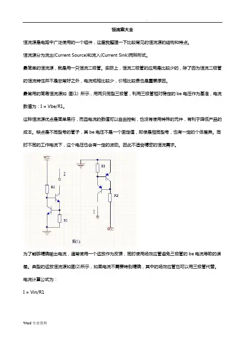
恒流案大全恒流源是电路中广泛使用的一个组件,这里我整理一下比较常见的恒流源的结构和特点。
恒流源分为流出(Current Source)和流入(Current Sink)两种形式。
最简单的恒流源,就是用一只恒流二极管。
实际上,恒流二极管的应用是比较少的,除了因为恒流二极管的恒流特性并不是非常好之外,电流规格比较少,价格比较贵也是重要原因。
最常用的简易恒流源如图(1) 所示,用两只同型三极管,利用三极管相对稳定的be电压作为基准,电流数值为:I = Vbe/R1。
这种恒流源优点是简单易行,而且电流的数值可以自由控制,也没有使用特殊的元件,有利于降低产品的成本。
缺点是不同型号的管子,其be电压不是一个固定值,即使是相同型号,也有一定的个体差异。
同时不同的工作电流下,这个电压也会有一定的波动。
因此不适合精密的恒流需求。
为了能够精确输出电流,通常使用一个运放作为反馈,同时使用场效应管避免三极管的be电流导致的误差。
典型的运放恒流源如图(2)所示,如果电流不需要特别精确,其中的场效应管也可以用三极管代替。
电流计算公式为:I = Vin/R1这个电路可以认为是恒流源的标准电路,除了足够的精度和可调性之外,使用的元件也都是很普遍的,易于搭建和调试。
只不过其中的Vin还需要用户额外提供。
从以上两个电路可以看出,恒流源有个定式(寒,“定式”好像是围棋术语XD),就是利用一个电压基准,在电阻上形成固定电流。
有了这个定式,恒流源的搭建就可以扩展到所有可以提供这个“电压基准”的器件上。
最简单的电压基准,就是稳压二极管,利用稳压二极管和一只三极管,可以搭建一个更简易的恒流源。
如图(3)所示:电流计算公式为:I = (Vd-Vbe)/R1TL431是另外一个常用的电压基准,利用TL431搭建的恒流源如图(4)所示,其中的三极管替换为场效应管可以得到更好的精度。
TL431组成流出源的电路,暂时我还没想到:)TL431的其他信息请参考《TL431的部结构图》和《TL431的几种基本用法》电流计算公式为:I = 2.5/R1事实上,所有的三端稳压,都是很不错的电压源,而且三端稳压的精度已经很高,需要的维持电流也很小。
各种LED恒流驱动及恒流IC芯片盘点LED恒流驱动简介由于LED是特性敏感的半导体器件,又具有负温度特性,因而在应用过程中需要对其进行稳定工作状态和保护,从而产生了驱动的概念。
LED器件对驱动电源的要求近乎于苛刻,LED不像普通的白炽灯泡,可以直接连接220V的交流市电。
LED是2~3伏的低电压驱动,必须要设计复杂的变换电路,不同用途的LED灯,要配备不同的电源适配器。
国际市场上国外客户对LED驱动电源的效率转换、有效功率、恒流精度、电源寿命、电磁兼容的要求都非常高,设计一款好的电源必须要综合考虑这些因数,因为电源在整个灯具中的作用就好比像人的心脏一样重要。
LED驱动电源把电源供应转换为特定的电压电流以驱动LED发光的电压转换器,通常情况下:LED驱动电源的输入包括高压工频交流(即市电)、低压直流、高压直流、低压高频交流(如电子变压器的输出)等。
而LED驱动电源的输出则大多数为可随LED正向压降值变化而改变电压的恒定电流源。
LED电源核心元件包括开关控制器、电感器、开关元器件(MOSFET)、反馈电阻、输入滤波器件、输出滤波器件等等。
根据不同场合要求、还要有输入过压保护电路、输入欠压保护电路,LED开路保护、过流保护等电路。
LED的恒流驱动用LED作为显示器或其他照明设备或背光源时,需要对其进行恒流驱动,主要原因是:1.避免驱动电流超出最大额定值,影响其可靠性。
2.获得预期的亮度要求,并保证各个LED亮度、色度的一致性3.能有效的避免雷击,电网的浪涌,过电流,过电压的保护,使LED寿命提高。
存在问题:要处理好散热问题,散热问题没有处理好就会影响LED寿命。
目前LED均采用直流驱动,因此在市电与LED之间需要加一个电源适配器即LED驱动电源。
它的功能是把交流市电转换成合适LED的直流电。
根据电网的用电规则和LED的驱动特性要求,在选择和设计LED驱动电源时要考虑到以下几点:1.高可靠性特别像LED路灯的驱动电源,装在高空,维修不方便,维修的花费也大。
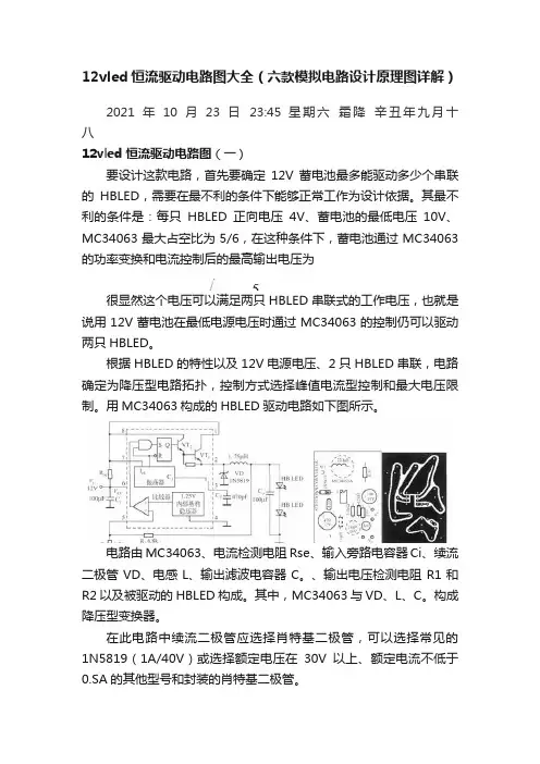
12vled恒流驱动电路图大全(六款模拟电路设计原理图详解)2021年10月23日23:45 星期六霜降辛丑年九月十八12vled恒流驱动电路图(一)要设计这款电路,首先要确定12V蓄电池最多能驱动多少个串联的HBLED,需要在最不利的条件下能够正常工作为设计依据。
其最不利的条件是:每只HBLED正向电压4V、蓄电池的最低电压10V、MC34063最大占空比为5/6,在这种条件下,蓄电池通过MC34063的功率变换和电流控制后的最高输出电压为很显然这个电压可以满足两只HBLED串联式的工作电压,也就是说用12V蓄电池在最低电源电压时通过MC34063的控制仍可以驱动两只HBLED。
根据HBLED的特性以及12V电源电压、2只HBLED串联,电路确定为降压型电路拓扑,控制方式选择峰值电流型控制和最大电压限制。
用MC34063构成的HBLED驱动电路如下图所示。
电路由MC34063、电流检测电阻Rse、输入旁路电容器Ci、续流二极管VD、电感L、输出滤波电容器C。
、输出电压检测电阻R1和R2以及被驱动的HBLED构成。
其中,MC34063与VD、L、C。
构成降压型变换器。
在此电路中续流二极管应选择肖特基二极管,可以选择常见的1N5819(1A/40V)或选择额定电压在30V以上、额定电流不低于0.SA的其他型号和封装的肖特基二极管。
上图电路中的输入电容器选择了100μF/16V的铝电解电容器,一般来说能够满足要求。
但是,从性能角度考虑,100μF/16V铝电解电容器的等效串联电阻至少为2Q,而50kHz频率下的容抗仅为31.8mΩ!容抗远低于等效串联电阻。
这时的电源旁路效果将取决于电容器的等效串联电阻,在0.25A交流电成分流过旁路电容器时,会在电源两端产生约0.SV有效值电压的交流成分,至少会产生1V(峰一峰值电压)的电压波动。
尽管这可以保证电路的正常工作,但使用起来还是感觉不那么舒服。
如果用封装为1206、介质为X5R的10μF/16V陶瓷贴片电容器(零售价约0.2元),则其等效串联电阻将低于lOmΩ,对应的容抗为0.318Q,总的阻抗低于100μF,远低于铝电解电容器的电容值,输入电源的电压尖峰将得到有效地抑制,可以降低到用铝电解电容器的1/10。
12ma 恒流源电路
恒流源电路是一种电子电路,用于产生恒定的电流输出。
它通常由电流源和负载组成。
在恒流源电路中,电流源的输出电流保持恒定,无论负载的变化。
这种电路在许多电子设备中都有广泛的应用,比如LED驱动、电池充电管理等。
恒流源电路的设计通常涉及使用电阻、晶体管或集成电路等元件。
其中,电流源可以采用电压控制电流源、电流镜电路、MOS管等来实现。
这些元件可以确保在一定的电压范围内,输出电流保持不变。
此外,负载的变化也不会对输出电流产生影响。
在实际应用中,恒流源电路可以用于稳定LED的亮度,保证电路中的传感器工作在恒定的电流下,以及在需要恒定充电电流的电池管理系统中。
此外,恒流源电路还可以用于一些精密仪器和测量设备中,以确保输出的电流稳定可靠。
总的来说,恒流源电路在电子电路设计中扮演着重要的角色,它能够稳定输出电流,保证电路正常工作,并在许多应用中发挥着重要作用。
灯带12v电压工作原理
灯带12V电压工作原理
简介
•12V电压是灯带常见的工作电压,其工作原理涉及到电路供电和发光二极管(LED)的特性。
以下将从两个方面进行解释。
电路供电
1.直流电源供电:灯带需要直流电源才能正常工作。
而12V直流电
源是常见的低电压供电方式,能提供足够的电能给灯带供电。
2.适配器:在实际应用中,由于家庭和商用环境的供电不一样,我
们通常需要使用适配器将交流电转换为适合灯带工作的直流电。
适配器将电压从220V(或110V)降压到12V,并通过电源线提供给灯带。
发光二极管(LED)特性
1.PN结:LED是一种半导体器件,内部由P型和N型半导体构成的
PN结。
当施加正向电压时,电子从N型区域向P型区域移动,同时空穴从P型区域向N型区域移动。
在PN结的边界处,电子和
空穴复合释放出能量,导致发光现象。
2.正向电压:为了使LED正常工作,需要施加比PN结的阈值电压
更高的正向电压。
对于大多数常见的LED,这个电压在2V至4V
之间。
而12V电压可以提供足够的正向电压以激活LED并使其发
光。
结语
•灯带在12V电压下工作的原理是基于电路供电和发光二极管(LED)的特性。
了解这些原理可以帮助我们更好地使用和理解灯带工作
时所需的电源和电路设计。
•注意:使用时请确保所使用的电源和电路设计符合相关安全标准,避免发生安全事故。
CL12/2410LG-A 升压恒流一体控制器使用说明一、功能简介:✧光控(时控)模式可设定开灯光照度和任意定时时间。
✧采用串联式的充电控制方式,使充电效率提高3%-6%,同时控制器MCT充电功能实时追踪太阳板的最大电流,充电方式更高效。
✧对于负载接入采用软启动方式,更好地保护了控制器和负载免受启动瞬间大电流的冲击。
✧全铝质机壳,多棱边的底板设计更是加大了散热面积,使整个控制器长期处于最佳的散热状态。
✧具有温度补偿功能,具有防雷击保护功能。
✧具有负载开路保护,短路保护及过温度保护。
✧蓄电池反接、太阳板反接、蓄电池反向放电保护功能。
✧欠压保护、过压保护和过流保护功能。
✧根据蓄电池容量自动智能化降低输出电流。
✧采用了宽电压输出设计,满足了不同种类的LED灯使用。
12V系统时,输出电压为15V-60V自适应,相当于常规的单颗1W灯珠5串-17串联电路通用;24V系统时,输出电压为30V-60V自适应,相当于常规的单颗1W灯珠10串-17串联电路通用。
✧温升智能保护功能。
✧采用了全密封完全防水的设计,使控制器稳定可靠性大幅提高。
✧无线连接电脑功能,如果配套本公司的红外编程遥控器使用,可以设置保护电压、开灯照度等多种参数,可以查询当前负载的功率以及故障、欠压次数,同时反映控制器当前运行状态,电池板、蓄电池的实时电压并且可以任意设置控制器的其他工作参数。
二、注意事项✧使用本控制器前,请确认控制器的工作参数已按您的要求设置好,避免因参数不匹配导致的部件损坏。
✧本控制器为宽电压输出,请在使用前,确认您的LED和控制器能匹配。
✧接线时,请严格按照顺序接线,错误的接线方法会导致系统误判或控制器的损坏。
✧本控制器为单路输出升压型恒流一体控制器,请将负载按正确的方式连接,否则可能导致负载或控制器的损坏。
三、接线方式✧先将负载的正负极接在控制器右边的两根红绿线上。
✧再将太阳板、蓄电池的正极,接在最左边的红线上。
✧然后把蓄电池的负极接在控制器的黑线上,大约10秒左右,控制器的负载灯亮,负载亮启,表明放电正常。
灯带12v电压工作原理灯带是一种广泛应用于室内装饰、景观照明等领域的照明产品。
它具有柔软、灵活、颜色丰富等特点,可以根据需要进行弯曲、剪裁和延长。
而灯带的工作原理是基于12V电压的。
灯带的主要组成部分是LED灯珠、电路板、电源等。
其中,LED灯珠是灯带的光源,电路板则是为LED提供电力和控制信号的载体,电源则是为整个灯带提供所需的电压。
在工作时,灯带的电源将12V直流电压转化为LED灯珠所需的电压。
常见的电源有电池、适配器和太阳能电池等。
这些电源经过一系列的电路处理,将输入的电压转化为稳定的直流电压,并通过电路板传递给LED灯珠。
LED灯珠是灯带的核心部件。
它采用半导体材料,通过电流的通过产生光。
在LED灯珠内部,有两个电极,分别为阳极和阴极。
当电流通过时,阳极和阴极之间的半导体材料会发生电子的跃迁,从而释放出能量,产生可见光。
通过控制电流的大小和频率,可以实现不同亮度和颜色的光效。
电路板起到了连接和控制LED灯珠的作用。
它上面有一系列的电路,包括电源、驱动电路和控制电路等。
电源电路负责将电源的电压转化为适合LED工作的电压;驱动电路用于提供稳定的电流,保证LED的正常工作;控制电路则可以通过调节电流和频率,实现对灯带亮度和颜色的控制。
总的来说,灯带的工作原理是通过电源将12V电压转化为适合LED 灯珠工作的电压,并通过电路板传递给LED灯珠。
LED灯珠通过电流的通过产生光,实现照明效果。
不同的电流和频率可以实现不同亮度和颜色的光效。
灯带的灵活性和多样性使其在室内装饰和景观照明中得到了广泛应用。
通过不同的控制方式,可以实现各种照明效果,为人们创造出舒适、温馨的照明环境。
12v适配器工作原理12V适配器工作原理适配器是一种将交流电转换为直流电的设备。
12V适配器是一种输出电压为12V的适配器,广泛应用于各种电子设备中。
下面将介绍12V适配器的工作原理。
1. 电源输入:12V适配器的输入端通常为交流电源,其电压一般为220V交流电。
交流电经过适配器的输入端后,进入到适配器的内部电路。
2. 整流滤波:适配器内部的整流滤波电路将输入的交流电转换为直流电。
整流电路通常由整流桥和电容器组成,整流桥将交流电的正半周和负半周分别转换为直流电,并通过电容器进行滤波,使输出电压更加稳定。
3. 变压器:在适配器的内部,还会有一个变压器。
变压器的作用是将输入电压变换为适合设备工作的电压。
对于12V适配器来说,变压器会将高压的直流电转换为12V的直流电输出。
4. 稳压电路:为了保证输出电压的稳定性,适配器中还会有一个稳压电路。
稳压电路根据输出电压的波动情况,调整电路中的元件,以保持输出电压的稳定。
5. 过载保护:为了保护设备和适配器本身,12V适配器还会设计过载保护电路。
当设备所需的电流超过适配器所能提供的最大电流时,过载保护电路会自动切断电源,以避免适配器过载损坏。
6. 绝缘和安全保护:在适配器的设计中,还会考虑到绝缘和安全保护的问题。
适配器的内部电路和外部电路之间会采取绝缘措施,以避免电气短路和触电危险。
此外,适配器还会通过一些安全保护装置,如过流保护和过热保护,来确保使用过程中的安全性。
总结:12V适配器的工作原理是将输入的交流电转换为输出的直流电,通过整流滤波、变压器、稳压电路等组成。
适配器还具备过载保护、绝缘和安全保护等功能,以确保设备和适配器本身的安全。
了解12V适配器的工作原理有助于我们更好地理解和使用适配器,同时也有助于我们在选购适配器时做出明智的选择。
12W High Precision CC/CV Primary-Side PWM DriverFEATURES◆ 5% Constant Voltage Regulation, 5%Constant Current Regulation at Universal AC input◆ Primary-side Sensing and Regulation Without TL431 and Opto-coupler ◆ Low Start-up Current: 5μA (Typical) ◆ Low Operating Current: 2mA (Typical) ◆ Programmable CV and CC Regulation ◆ Adjustable Constant Current and Output Power Setting◆ Built-in Secondary Constant CurrentControl with Primary Side Feedback ◆ Peak-Current-Mode Control◆ Compensates for transformer inductance tolerances◆ Compensates for cable voltage drop ◆ Fixed PWM Frequency at 60kHz withFrequency Hopping to Solve EMI Problems ◆ Power on Soft-start◆ Built-in Leading Edge Blanking (LEB) ◆ Cycle-by-Cycle Current Limiting ◆ VDD Under-Voltage lockout (UVLO) ◆ VDD Over-Voltage Protection(OVP)APPLICATIONSbelow 12W AC/DC offline SMPS for ◆ Cell Phone Charger◆ Digital Cameras Charger ◆ Small Power Adapter◆ Auxiliary Power for PC, TV etc.◆ Linear Regulator/RCC ReplacementCL1112 is offered in SOP-8 and DIP-8 package.TYPICAL APPLICATIONSPin ConfigurationThe pin map is shown as below for SOP8/DIP8CL1112CL1112GENERAL DESCRIPTIONCL1112 is a high performance offline PWM driver for low power AC/DC charger and adaptor applications. It operates in primary-side sensing and regulation. Consequently, opto-coupler andTL431 could be eliminated. Proprietary Constant Voltage (CV) and Constant Current(CC) controlis integrated as shown in the figure below.In CC control, the current and output power setting can be adjusted externally by the sense resistor Rs at CS pin. In CV control, multi-mode operations are utilized to achieve high performance and high efficiency. In addition, good load regulation is achieved by the built-in cabledrop compensation. Device operates in PFM in CC mode as well at large load condition and it operates in PWM with frequency reduction at light/medium load. CL1112 offers power on soft start control and protection coverage with auto-recovery features including Cycle-by-Cycle current limiting, VDD OVP, VDD clamp and UVLO. Excellent EMI performance is achieved with frequency jittering technique. High precision constant voltage (CV) and constant current (CC) can be achieved by CL1112.Fig.1. Typical CC/CV CurveCL1112 PACKAGE DISSIPATION RATINGPackage RθJA (℃/W) MarkingCL1112S SOP8 90CL1112D DIP8 40ABSOLUTE MAXIMUM RATINGS (note1)Parameter VALUEDrain Voltage (off state) -0.3V to BvdssVDD Voltage -0.3 to VDD_clamp10 mAVDD Zener ClampContinuous CurrentCOMP Voltage -0.3 to 7VCS Input Voltage -0.3 to 7VFB Input Voltage -0.3 to 7VMin/Max Operating-20 to 150 CJunction Temperature TJ-55 to 150 CMin/Max StorageTemperature Tstg260 o CLead Temperature(Soldering, 10secs)Note: Stresses beyond those listed under “absolute maximum ratings” may cause permanentdamage to the device. These are stress ratings only, functional operation of the device at these orany other conditions beyond those indicated “recommended operating conditions” is not implied.Exposure to absolute maximum-rated conditions for extended periods may affect device reliability.TERMINAL ASSIGNMENTSPin NumPin Name I/O Description1 VDD P Power Supply2COMPILoop Compensation for CV Stability3 FB IThe voltage feedback from auxiliary winding. Connected to resistor divider from auxiliary winding reflecting outputvoltage. PWM duty cycle is determined by EA output and current sense signal at pin 4.4 CS I Current sense input 5/6 DRAIN OHV MOSFET Drain Pin. The Drain pin is connected to the primary lead ofthe transformer 7/8 GND P GroundBLOCK DIAGRAMCompFBCSDRAINGNDCL1112ELECTRICAL CHARACTERISTICS(TA = 25℃, VDD=16V, if not otherwise noted)Symbol Parameter TestConditionsMinTyp.Max.Unit Supply Voltage (VDD) SectionI DD ST StandbyCurrent V DD=13V520uAI DD op OperationCurrent Operation supplycurrent FB=2V, CS=0V,VDD=VDDG=20V- 2.5 3.5 mAUVLO(ON) V DD Under Voltage LockoutEnterV DD falling 7.58.510VUVLO(OFF) V DD Under Voltage LockoutExitV DD rising 13.514.516.0VV DD_clamp Maximum V DD operationvoltageI DD=10mA 30.532.534.5VOVP Over voltage protectionThresholdRamp VDD until gateshut down27.5 29.5 31.5 VCurrent Sense Input SectionTLEB LEBtime 540 ns V th_oc Over current threshold 870 900 930 mVTd_oc OCPPropagationdelay 150 ns Z SENSE_IN InputImpedance 50 KohmT_ss Softstarttime 10 ms Frequency SectionFreq_Max NoteIC Maximum frequency 65 70 75 kHzFreq_Nom System Nominal switchfrequency60KHzFreq_startup FB=0V, Comp=5V 14 KHz f/Freq Frequency shuffling range +/-4 % Error Amplifier sectionVref_EA Reference voltage for EA 1.97 2 2.03 V Gain DC gain of EA 60 dBI_COMP_M AX Max.Cable compensationcurrentFB=2V, Comp=0V 42 uAPower MOSFET SectionBVdss MOSFET Drain-SourceBreakdown Voltage600 VRdson OnResistance Static,Id=0.4A 12 15 ΏNote:1. Freq_Max indicates IC internal maximum clock frequency. In system application, the maximum operation frequency of 70Khz nominal occurs at maximum output power or the transition point fromCV to CC.CL1112Application InformationOperation OverviewThis highly integrated PSR PWM controller contains several features to enhance the performance of low-power flyback converters. The patented topology of the PSR controller allows for simplified of circuit designs, particularly battery charger applications. It operates in primary side sensing and regulation, thus opto-coupler and TL431 are not required. CV and CC control can be accurately achieved without secondary feedback circuitry. A frequency jittering function is built in to improve EMI system performance. As a result, a low-cost, smaller, and lighter charger is produced when compared to a conventional design or a linear transformer.Under Voltage Lockout (UVLO)An UVLO comparator is implemented to detect the voltage of VDD pin. It would assure the supply voltage enough to turn on the CL1112 PWM controllers and further to drive the power MOSFET. A hysterics is built in to prevent the shutdown from the voltage dip during startup. The turn-on and turn-off threshold level are set at 14.8V and 9V, respectively.Soft StartCL1112 incorporates an internal soft-start function with no external components to minimize the component electrical over-stress during power on startup. The soft-start time is set at 17ms. As soon as VDD reaches UVLO (OFF), the control algorithm will ramp peak current voltage threshold gradually from nearly zero to normal setting of 0.90V. Every restart is a soft start.CC/CV OperationCL1112 is designed to produce good CC/CV control characteristic as shown in the Fig. 1.Battery chargers are typically designed for two modes of operation, constant-voltage charging and constant-current charging. When the battery voltage is low, the charger operates on a constant current charging. This is the main method for charging batteries and most of the charging energy is transferred into the batteries. When the battery voltage reaches its end-of-charge voltage, the current begins to taper-off. The charger then enters the constant voltage method of charging. Finally, the charging current continues to taper-off until reaching zero.Output Voltage settingThe CL1112 monitors the auxiliary fly-back signal from FB pin through a resistor divider pair of Ra and Rb. An error signal, which represents the difference between the voltage at FB and the reference voltage, is integrated with the error amplifier to control switching duty cycle.The output voltage is determined by the following relationship. For improving the output voltage accuracy, the transformer leakage inductance should be reduced as much as possible.a sOUT b aR N V 2V(1)()R N =+Where,Ra and Rb are the top and bottom feedback resistor value,Ns and Na are the turn ratios of transformer secondary and auxiliaryThe load regulation and line regulation for primary side feedback control are sensitive to the structure of transformer. For getting good regulation and efficiency, the sandwich structure consisting of two secondary separate parallel layer windings surrounding primary winding isCL1112CL1112recommended.Inductance Correction CircuitryIf the primary magnetizing inductance is either too high or low the converter will automatically compensate for this by adjusting the oscillator frequency. Since this controller is designed to operate in discontinuous-conduction mode the output power is directly proportional to the set primary inductance and its tolerance can be completely compensated with adjustments to the switching frequency.Frequency TremblingThe CL1112 is implemented with an adjustable modulating frequency for trembling function, which enable the power supply designers to achieve optimized EMI performance and excellent systemcost. The trembling frequency is internally fixed between ±3.6KHz to incorporate with the 65KHz switching frequency.Current Sensing and Leading EdgeBlanking Cycle-by-Cycle current limiting is offered in CL1112. The switch current is detected by asense resistor into the CS pin. When the power switch is turned on, a turn-on spike will occur on thesense-resistor. To avoid false-termination of the switching pulse, 625ns leading-edge blanking isbuilt in. During this blanking period, the current sense comparator is disabled and the gate drivercan not be switched off.Programmable Cable drop CompensationIn CV regulation control, the on-time of MOSFET only regulates on-board voltage, not includingoutput cable. Different cable wire gauge or length results in different output voltage. The CL1112has a cable compensation function used to compensate the output voltage drop due to output cableloss. An offset voltage is generated at FB by an internal current flowing into the resister divider. Asthe converter load increases from no-load to the peak power point (transition point between CV andCC) the voltage drop introduced across the output cable is compensated by increasing internal current flowing into the resister divider.Protection ControlGood power supply system reliability is achieved with its rich protection features includingCycle-by-Cycle current limiting (OCP), VDD clamp, Power on Soft Start, and Under Voltage Lockout on VDD (UVLO). VDD is supplied by transformer auxiliary winding output. The output ofCL1112 is shut down when VDD drops below UVLO (ON) limit and the power converter enterspower on start-up sequence thereafter.z The information described herein is subject to change without notice.z is not responsible for any problems caused by circuits or diagrams described hereinwhose related industrial properties, patents, or other rights belong to third parties. The application circuit examples explain typical applications of the products, and do not guarantee the success of any specific mass-production design.z When the products described herein are regulated products subject to the WassenaarArrangement or other agreements, they may not be exported without authorization from the appropriate governmental authority.z Use of the information described herein for other purposes and/or reproduction or copyingwithout the express permission of is strictly prohibited. z The products described herein cannot be used as part of any device or equipment affecting thehuman body, such as exercise equipment, medical equipment, security systems, gas equipment, or any apparatus installed in airplanes and other vehicles, without prior written permission of z Although exerts the greatest possible effort to ensure high quality and reliability, the failure or malfunction of semiconductor products may occur. The user of these products should therefore give thorough consideration to safety design, including redundancy, fire-prevention measures, and malfunction prevention, to prevent any accidents, fires, or community damage that may ensue.SANY SemiconductorSANY SemiconductorSANY SemiconductorSANY SemiconductorCL1112。