SP504AN中文资料
- 格式:pdf
- 大小:181.55 KB
- 文档页数:11

USER MANUAL MODEL 504 & 505Surge ProtectedDB-25 to Modular Adapters SALES OFFICE (301) 975-1000TECHNICAL SUPPORT (301) 975-1007Part#07M504/505-C Doc# 074241U,Rev. D Revised 1/21/08C E R T I F I E D An ISO-9001Certified Company1.0 WARRANTY INFORMATIONPatton Electronics warrants all Model 504 & 505 components to be free from defects, and will—at our option—repair or replace the product should it fail within one year from the first date of shipment. This warranty is limited to defects in workmanship or materials, and does not cover customer damage, abuse or unauthorized modification. If this product fails or does not perform as warranted, your sole recourse shall be repair or replacement as described above. Under no condition shall Patton Electronics be liable for any damages incurred by the use of this product. These damages include, but are not limited to, the following: lost profits, lost savings and incidental or consequential damages arising from the use of or inability to use this product. Patton Electronics specifically disclaims all other warranties, expressed or implied, and the installation or use of this product shall be deemed an acceptance of these terms by the user.1.1 RADIO AND TV INTERFERENCEThe Model 504 & 505 Series units generate and use radio frequency energy, and if not installed and used properly—that is, in strict accordance with the manufacturer's instructions—may cause interference to radio and television reception. They have been tested and found to comply with the limits for a Class A computing device in accordance with the specifications in Subpart J of Part 15 of FCC rules, which are designed to provide reasonable protection from such interference in a commercial installation. However, there is no guarantee that interference will not occur in a particular installation. If these products do cause interference to radio or television reception, which can be determined by turning off the unit, the user is encouraged to try to correct the interference by one or more of the following measures: moving the computing equipment away from the receiver, re-orienting the receiving antenna and/or plugging the receiving equipment into a different AC outlet (such that the computing equipment and receiver are on different branches).1.2 CE NOTICEThe CE symbol on your Patton Electronics equipment indicates that it is in compliance with the Electromagnetic Compatibility (EMC) directive and the Low Voltage Directive (LVD) of the Union European (EU). A Certificate of Compliance is available by contacting Technical Support.1All warranty and nonwarranty repairs must be returned freight prepaid and insured to Patton Electronics. All returns must have a Return Materials Authorization number on the outside of the shipping container. This number may be obtained from Patton Electronics Technical Support: (301) 975-1007; ; or,******************.NOTE: Packages received without an RMA number will not beaccepted.Patton Electronics' technical staff is also available to answer any questions that might arise concerning the installation or use of yourPatton Model 504 & 505. Technical Service hours: 8AM to 5PM EST,Monday through Friday.2Dear Valued Customer,Thank you for purchasing Patton Electronics products! We do appreciate your business. I trust that you find this user manual helpful.We manufacture one of the widest selections of data communications products in the world including CSU/DSU's, network termination units, powered and self-powered short range modems, fiber optic modems, interface converters, baluns, electronic data switches, data-line surge protectors, multiplexers, transceivers, hubs, print servers and much more. We producethese products at our Gaithersburg, MD, USA, facility, and can custom manufacture products for your unique needs.We would like to hear from you. Please contact us in any of the following ways to tell us how you like this product and how we can meet your product needs today and in the future.Web: Sales E-mail: ****************Support E-mail: ******************Phone - Sales (301) 975-1000Phone - Support (301) 975-1007Fax: (301) 869-9293Mail: Patton Electronics Company7622 Rickenbacker DriveGaithersburg, MD 20879 USAWe are committed to a quality product at a quality price. Patton Electronics is ISO 9001 certified. We meet and exceed the highest standards in the industry (CE, UL, etc.).It is our business to serve you. If you are not satisfied with any aspect of this product or the service provided from Patton Electronics or its distributors, please let us know.Thank you.Burton A.PattonVice PresidentP.S. Please tell us where you purchased this product:__________________________________________________________________________________________________________________ _________________________________________________________ _________________________________________________________ _________________________________________________________ _________________________________________________________。


■Operates from Single +5V Power Supply ■Meets All RS-232D and V.28 Specifications ■±9V Output Swing with +5V Supply ■Improved Driver Output Capacity for Mouse Applications■Low Power Shutdown – 1µA■WakeUp Feature in Shutdown Mode ■3–State TTL/CMOS Receiver Outputs ■±30V Receiver Input Levels■Low Power CMOS – 5mA Operation ■Wide Charge Pump Capacitor Value Range – 1-10µFDESCRIPTION…The SP230A Series are multi–channel RS-232 line drivers/receivers that provide a variety of configurations to fit most communication needs, especially where ±12V is not available. Some models feature a shutdown mode to conserve power in battery-powered systems. Some require no external components. All, except one model, feature a built-in charge pump voltage converter, allowing them to operate from a single +5V power supply. All drivers and receivers meet all EIA RS-232D and CCITT V.28 requirements. The Series is available in plastic DIP and SOIC packages.SELECTION TABLET OUT T OUT T IN T IN V- C - C + C -34221T OUT T OUT T IN T IN GND V C + V+12CC 12134Now Available in Lead Free Packaging元器件交易网ABSOLUTE MAXIMUM RATINGS This is a stress rating only and functional operation of the device at these or any other conditions above those indicated in the operation sections of this specification is not implied. Exposure to absolute maximum rating conditions for extended periods of time may affect reliability.VCC ...............................................................................................................................................................+6VV+...................................................................................................................(Vcc–0.3V) to +13.2V V–.............................................................................................................................................................13.2V Input Voltages:T IN .......................................................................................................................–0.3 to (Vcc +0.3V)RIN ............................................................................................................................................................±30VOutput Voltages:TOUT.................................................................................................(V+, +0.3V) to (V–, –0.3V)ROUT..............................................................................................................–0.3V to (Vcc +0.3V)Short Circuit Duration:TOUT.........................................................................................................................................ContinuousPower Dissipation:CERDIP..............................................................................675mW(derate 9.5mW/°C above +70°C)Plastic DIP..........................................................................375mW(derate 7mW/°C above +70°C)Small Outline......................................................................375mW(derate 7mW/°C above +70°C)ELECTRICAL CHARACTERISTICS元器件交易网0V 5V 0V5V 0V0VT INT INT OUTT OUTR L = 3k Ω, C L = 2,500pFNo loadTransmitter Propagation DelayTransmitter Output WaveformsReceiver Output WaveformShutdown to V+, V– Rise TimeInOut5V 0V 0VSDV +V –Rise TimeR L = 3k Ω; C L = 2,500pF All inputs = 20kHzT INT OUTT INT OUTFall TimeR L = 3k Ω; C L = 2,500pFReceiver Propagation DelayRIN 5V 0VR OUT5V 0VR IN5V 0VR OUTPINOUTFall Time Rise TimeReceiver Output Enable/Disable TimesDisable5V 0V5V 0VEN INR OUTEnable5V 0V5V 0VEN INR OUTPINOUTFEATURES…The multi–channel RS-232 line drivers/receivers pro-vides a variety of configurations to fit most communi-cation needs, especially those applications where ±12V is not available. The SP230A, SP235A/B, SP236A/B, SP240A/B, and SP241A/B feature ashutdown mode which reduces device power dissipa-tion to less than 5µW. All feature low power CMOS operation, which is particularly beneficial in battery-powered systems. The SP235A/B use no external components and are ideally suited where printed circuit board space is limited.All products in the Series include two charge pump voltage converters which allow them to operate from a single +5V supply. These converters convert the +5V input power to the ±10V needed to generate the RS-232 output levels. An internal charge pump converter produces the necessary –12V supply. All drivers and receivers meet all EIA RS-232D and CCITT V.28 specifications.The Series are available for use over the commer-cial, industrial and military temperature ranges. They are packaged in plastic DIP and SOIC packages. For product processed and screened to MIL–M–38510 and MIL–STD–883C require-ments, please consult the factory.THEORY OF OPERATIONThe SP230A/B–241A/B series devices are made up of t hree b asic c ircuit b locks –1) t ransmitter, 2) r eceiver and 3) charge pump. Each model within the series incorporates variations of these circuits to achieve the desired configuration and performance.Driver/TransmitterThe drivers are inverting transmitters, which accept TTL or CMOS inputs and output the RS-232 signals with an inverted sense relative to the input logic levels. Typically the RS-232 output voltage swing is ±9V. Even under worst-case loading conditions of 3kΩand 2500pF, the output is guaranteed to be ±5V, which is consistent with the RS-232 standard specifications. The transmitter outputs are protected against infi-nite short-circuits to ground without degradation in reliability.The drivers of the SP230A, SP235A/B, SP236A/B, SP240A/B and SP241A/B can be tri-stated by using the SHUTDOWN function. In this “power-off” state, the output impedance will remain greater than 300 Ohms, again satisfying the RS-232 specifications. Should the input of the driver be left open, an internal 400kΩ pull–up resistor to VCCforces the input high, thus committing the output to a low state.The slew rate of the transmitter output is internally limited to a maximum of 30V/µs in order to meet theTable 1. EIA Standards Definition 元器件交易网Charge Pump Output Loading versus VCC; a) V+; b) V–ENABLE Input (EN)The SP235A/B , SP236A/B , SP240A/B, and SP241A/B all feature an enable input (EN),which allows the receiver outputs to be either tri–stated or enabled. The enable input is active outputs. This can be especially useful when the receiver is tied directly to a microprocessor data bus.Protection From Shorts to >±15VThe driver outputs are protected against shorts to ground, other driver outputs, and V + or V -.For protection against voltages exceeding ±15V,two back–to–back zener diodes connected to clamp the outputs to an acceptable voltage level are recommended. (Refer to Figure 3.)Improved Drive Capability for Mouse ApplicationsEach of the devices in this data sheet have improved drive capability for non-standard ap-plications. Although the EIA RS-232D stan-dards specify the maximum loading to be 3k Ωand 2500pF, the SP230A , SP234A , SP235A/B ,SP236A/B , SP237A , SP238A , SP240A/B, and SP241A/B can typically drive loads as low as 1k Ω and still maintain ±5V outputs. This feature is especially useful when the serial port is in-tended to be used for a “self-powered” mouse.In this case the voltage necessary to operate the circuits in the mouse can be derived from the RS-232 driver output as long as the loading is ≥1k Ω (refer to Figure 4). For applications which even exceed this requirement, drivers can be connected in parallel, increasing the drive capa-bility to 750Ω, while maintaining the ±5V V OH and V OL levels (refer to Figure 5).Figure 3. High Voltage Short Circuit ProtectionFigure 2. Charge Pump Voltage Inverter output impedance of V + and V -, which will degrade V OH and V OL . Capacitor values can be as low as 1.0µF.Shutdown (SD)The SP230A , SP235A/B , SP236A/B , SP240A/B and SP241A/B all feature a control input which will disable the part and reduce V CC current typically to less than 5µA, which is especially useful to designers of battery–pow-ered systems. In the “power–off” mode the receiver and transmitter will both be tri-stated.V + will discharge to V CC , and V - will discharge to ground.For complete shutdown to occur and the 10µA current drain to be realized, the following con-ditions must be met:• +5.00V must be applied to the SD pin;• ENABLE must either 0V, +5.0V or not connected;• the transmitter inputs must be either +5.0V or not connected;• V CC must be +5V;• Receiver inputs must be >0V and <+5VPlease note that for proper operation, the SD input pin must never be left floating.Table 2. Wake–Up Truth TableFigure 4. Mouse Application Drive Capability 10 9 8 7 6 5 4 3 2 1 0V O L /V O H (V o l t s )246810121820I OL /I OH (mA)161422V OL vs I OLV OH vs I OHFigure 5. Parallel DriversWake-Up FeatureThe SP235B , SP236B , SP240B and SP241B have a wake-up feature that keeps all receivers in an enabled state when the device is in the shutdown mode. Table 2 defines the truth table for the wake-up function. Timing for the wake-up function is shown in Figure 6.If the SP235B , SP236B , SP240B and SP241B are powered up in the shutdown state (SD driven high during V CC power up), the part must remain in a powered on state for a minimum of 3ms before the wake-up function can be used. After the 3ms wait time, there is a 2ms delay time before data is valid for both enable and disableFigure 6. Wake–Up and Shutdown Timing元器件交易网of the charge pump. If the SP2XXB is powered up with SD low, then only the 2ms delay time will apply (refer to Figure 6). Under normal operation, both the wait time and delay time should be transparent to the user.With only the receivers activated, the device typically draws less than 5µA (10µA max) sup-ply current. In the case of a modem interfaced to a computer in power-down mode, the RI (ring indicator) signal from the modem would be used to “wake up” the computer, allowing it to accept the data transmission.After the ring indicator signal has propagated through the SP2XXB receiver, it can be used to trigger the power management circuitry of the computer to power up the microprocessor and bring the SD pin to the SP2XXB low, taking it out of shutdown. The receiver propagation de-lay is typically 1µs. The enable time for V+ and V- is typically 2ms. After V+ and V- have settled to their final values, a signal can be sent back to the modem on the DTR (Data Terminal Ready) pin signifying that the computer is ready to accept and transmit data.All receivers that are active during shutdown maintain 500mV (typ.) of hysteresis.Varying Capacitor ValuesAs stated earlier, the capacitor values are some-what non-critical. Since they are an actual compo-nent of the charge pump circuitry, their value will affect its performance, which in turn affects the V OH and V OL levels. There is no upper limit for the value of any of the four capacitors; lower values will impact performance. C 1 and C 2 are respon-sible for the charge accumulation and can be reduced to 1µF; this will increase the output im-pedance of V + and V –. Reducing these capacitor values will limit the ability of the SP2XXA/B to maintain the dc voltages needed to generate the RS-232 output levels. Capacitors C 3 and C 4 can also be reduced to 1µF; doing so will increase the ripple on V + and V–.Typically each driver will require 1µF of capaci-tance as a minimum to operate within all specified parameters; if five drivers are active in the circuit,then C 3 and C 4 should be 5µF. In order to operateat these minimum values, the supply voltage must be maintained at +5.0V ±5%. Also, the ambient operating temperature must be less than 60°C.The capacitor values must be chosen to suit the particular application. The designer must bal-ance board space, cost and performance to maxi-mize the design. The capacitors can be polarized or non–polarized, axial-leaded or surface-mount.As the size and value decrease, so does the cost;however, the value should be chosen to accom-modate worst-case load conditions.IBM Modem Port InterconnectionsINTERFACE EXAMPLE – A MODEM ON THE IBM PC SERIAL PORTThe RS-232 standard defines 22 serial interface signals. These signals consist of ground lines,timing, data, control and test signals, plus a set of signals rarely used for a second data channel.Many of these signal lines are not used in typical RS-232 applications; in fact, the IBM ® PC serial port is implemented using only nine pins.For example, consider the case of a PC using this nine pin port to communicate with a peripheral device such as a modem. We see the following activity on each of the RS-232 lines as the computer and modem are activated and commu-nicate with each other as well as the remote modem at the other end of the phone line.Signal Ground (GND)The Signal Ground pin acts as a reference for all the other signals. This pin is simply maintained at a 0V level to serve as a level to which all other signals are referenced. Both the PC and the modem will have this line connected to their respective internal ground lines.元器件交易网Data Terminal Ready (DTR)This is the pin the computer uses to tell periph-eral devices that it is on–line and ready to communicate.Data Set Ready (DSR)Peripheral devices use this line to tell the com-puter that they are on–line and ready to commu-nicate. When the modem is turned on and has completed its self–test routine (assuming it does one), it will send a signal to the PC by asserting this line.Request To Send (RTS)The computer activates this line to notify the peripheral device that it is ready to send data. In this example, the computer notifies the modem that it is ready to send data to be transmitted by the modem.Clear To Send (CTS)This is the line on which the peripheral device tells the computer that it is ready to receive data from the computer. If the modem was not ready, i.e. it was performing a loop–back self–test, for example, it would not assert this line. Once the modem was ready to receive data from the PC, it would assert this line. When it receives the CTS signal from the modem, the PC knows that a data transmission path has been established between itself and the modem.Transmitted Data (TD or TX)This is the pin on which the computer sends the actual data signal to be transmitted, i.e. a posi-tive voltage (+3V to +15V) to represent a logic “0”, and a negative voltage (–3V to –15V) to represent a logic “1”. The PC would send the data on this line to be transmitted by the modem. Ring Indicator (RI)This line is used by the peripheral device to tell the computer that a remote device wants to start communicating. The modem would activate the RI line to tell the computer that the remote modem was calling, i.e. the phone is ringing. Data Carrier Detect (DCD)This line is used by the modem to tell the computer that it has completed a transmission path with the remote modem, and to expect to start receiving data at any time.Received Data (RD or RX)This is the pin on which the modem sends the computer the incoming data signal, i.e. a posi-tive voltage (+3V to +15V) to represent a logic “0”, and a negative voltage (-3V to -15V) to represent a logic “1”.INTERFACE EXAMPLE – A PRINTER ON THE IBM PC SERIAL PORTThe RS-232 standard defines 22 serial interface signals. These signals consist of ground lines, timing, data, control and test signals, plus a set of signals rarely used for a second data channel. Many of these signal lines are not used in typical RS-232 applications; in fact, the IBM® PC serial port is implemented using only nine pins.For example, consider the case of a PC using this nine pin port to communicate with a peripheral device such as a printer. We see the following activity on each of the RS-232 lines as the com-puter and printer are activated and communicate. Signal Ground (GND)The Signal Ground pin acts as a reference for all the other signals. This pin is simply maintained at a 0V level to serve as a level to which all other signals are referenced. Both the PC and the printer will have this line connected to their respective internal ground lines.Data Terminal Ready (DTR)This is the pin the computer uses to tell peripheral devices that it is on–line and ready to communi-IBM Printer Port Interconnections元器件交易网cate. Once the computer is powered–up and ready, it will send out a signal on the DTR to inform the printer that it is powered–up and ready to go. The printer really doesn’t care, since it will simply print data as it is received. Accordingly, this pin is not needed at the printer.Data Set Ready (DSR)Peripheral devices use this line to tell the computer that they are on–line and ready to communicate. When the printer is turned on and has completed its self–test routine (assuming it does one), it will send a signal to the PC by asserting this line. Request To Send (RTS)The computer activates this line to notify the peripheral device that it is ready to send data. In this example, the computer notifies the printer that it is ready to send data to be printed by the printer. Clear To Send (CTS)This is the line on which the peripheral device tells the computer that it is ready to receive data from the computer. If the printer was not ready, i.e. it was out of paper, for example, it would not assert this line. Once the printer was ready to receive data from the PC, it would assert this line. When it receives the CTS signal from the printer, the PC knows that a data transmission path has been established between itself and the printer. Transmitted Data (TD or TX)This is the pin on which the computer sends the actual data signal representing the actual informa-tion to be printed, i.e. a positive voltage (+3V to +15V) to represent a logic “0”, and a negative voltage (-3V to -15V) to represent a logic “1”. Ring Indicator (RI)This line is used by the peripheral device to tell the computer that a remote device wants to start com-municating. A modem would activate the RI line to tell the computer that a remote modem was calling, i.e. the phone is ringing. In the case of a printer, this line is unused.Data Carrier Detect (DCD)This line is used by a peripheral device to tell the computer to expect to start receiving data at any time. Since the printer would not be sending data to the PC in this case this line is not needed.Received Data (RD or RX)This is the pin on which the computer receives the incoming data signal, i.e. a positive voltage (+3V to +15V) to represent a logic “0”, and a negative voltage (-3V to -15V) to represent a logic “1”. Again, in this instance, since the printer will not be sending the PC any data, this line is not needed.元器件交易网ORDERING INFORMATIONModel .......................................................................................Temperature Range....................................................................PackageSP230ACP .....................................................................................0°C to +70°C ...............................................................................20 pin PDIP SP230ACT .....................................................................................0°C to +70°C ............................................................................20 pin WSOIC SP230ACT/TR ...............................................................................0°C to +70°C ............................................................................20 pin WSOIC SP230ACX .....................................................................................0°C to +70°C ............................................................................................Dice SP230AEP ...................................................................................–40°C to +85°C .............................................................................20 pin PDIP SP230AET ...................................................................................–40°C to +85°C ..........................................................................20 pin WSOIC SP230AET/TR .............................................................................–40°C to +85°C ..........................................................................20 pin WSOIC SP234ACP .....................................................................................0°C to +70°C ...............................................................................16 pin PDIP SP234ACT .....................................................................................0°C to +70°C ............................................................................16 pin WSOIC SP234ACT/TR ...............................................................................0°C to +70°C ............................................................................16 pin WSOIC SP234ACX .....................................................................................0°C to +70°C ............................................................................................Dice SP234AEP ...................................................................................–40°C to +85°C .............................................................................16 pin PDIP SP234AET ...................................................................................–40°C to +85°C ..........................................................................16 pin WSOIC SP234AET/TR .............................................................................–40°C to +85°C ..........................................................................16 pin WSOIC SP235ACP .....................................................................................0°C to +70°C ...............................................................................24 pin PDIP SP235AEP ...................................................................................–40°C to +85°C .............................................................................24 pin PDIP SP235BCP .....................................................................................0°C to +70°C ...............................................................................24 pin PDIP SP235BEP ...................................................................................–40°C to +85°C .............................................................................24 pin PDIP SP236ACS .....................................................................................0°C to +70°C ...............................................................................24 pin PDIP SP236ACT .....................................................................................0°C to +70°C ............................................................................24 pin WSOIC SP236ACT/TR ...............................................................................0°C to +70°C ............................................................................24 pin WSOIC SP236ACX .....................................................................................0°C to +70°C ............................................................................................Dice SP236AES ...................................................................................–40°C to +85°C .............................................................................24 pin PDIP SP236AET ...................................................................................–40°C to +85°C ..........................................................................24 pin WSOIC SP236AET/TR .............................................................................–40°C to +85°C ..........................................................................24 pin WSOIC SP236BCS .....................................................................................0°C to +70°C .............................................................................. 24 pin PDIP SP236BCT .....................................................................................0°C to +70°C ............................................................................24 pin WSOIC SP236BCT /TR ..............................................................................0°C to +70°C ............................................................................24 pin WSOIC SP236BCX .....................................................................................0°C to +70°C ............................................................................................Dice SP236BES ...................................................................................–40°C to +85°C .............................................................................24 pin PDIP SP236BET ...................................................................................–40°C to +85°C ..........................................................................24 pin WSOIC SP236BET /TR ............................................................................–40°C to +85°C ..........................................................................24 pin WSOIC SP237ACS .....................................................................................0°C to +70°C ...............................................................................24 pin PDIP SP237ACT .....................................................................................0°C to +70°C ............................................................................24 pin WSOIC SP237ACT/TR ...............................................................................0°C to +70°C ............................................................................24 pin WSOIC SP237ACX .....................................................................................0°C to +70°C ............................................................................................Dice SP237AES ...................................................................................–40°C to +85°C .............................................................................24 pin PDIP SP237AET ...................................................................................–40°C to +85°C ..........................................................................24 pin WSOIC SP237AET/TR .............................................................................–40°C to +85°C ..........................................................................24 pin WSOIC/TR = Tape and ReelPack quantity is 1,500 for WSOIC.Available in lead free packaging. To order add "-L" suffix to part number.Example: SP230AEP = standard; SP230AEP-L = lead free Please consult factory for SP235B, SP236B, SP240B, SP241B, and dice.CorporationANALOG EXCELLENCESipex Corporation Headquarters and Sales Office233 South Hillview Drive Milpitas, CA 95035TEL: (408) 934-7500FAX: (408) 935-7600元器件交易网。


![压力检测器及其相关的显示模组[发明专利]](https://img.taocdn.com/s1/m/4371a93fce2f0066f433225f.png)
专利名称:压力检测器及其相关的显示模组专利类型:发明专利
发明人:贡振邦
申请号:CN201510434883.1
申请日:20150722
公开号:CN105487703A
公开日:
20160413
专利内容由知识产权出版社提供
摘要:本发明实施例公开了一种显示模组,包括:一前面板,是由复数个显示像素所组成的一阵列;一背光面板,位于该前面板下方;一压力检测器,位于该背光面板下方;以及一机构中框,位于该压力检测器下方;其中,该前面板接收一施加压力,使得该压力检测器根据该施加压力获得一受力大小。
申请人:敦泰电子有限公司
地址:开曼群岛大开曼KY1-1112号2804号信箱板球广场绿柳大厦四层
国籍:KY
代理机构:北京集佳知识产权代理有限公司
代理人:王宝筠
更多信息请下载全文后查看。

Rev. EDocument FeedbackInformation furnished by Analog Devices is believed to be accurate and reliable. However, no responsibility is assumed by Analog Devices for its use, nor for any infringements of patents or other rights of third parties that may result from its use. Specifications subject to change without notice. No license is granted by implication or otherwise under any patent or patent rights of Analog Devices. Trademarks andregistered trademarks are the property of their respective owners.One Technology Way, P .O. Box 9106, N orwood, MA 02062-9106, U.S.A.Tel: 781.329.4700 ©2007-2020 Analog Devices, Inc. All rights reserved. Technical Support /cnADI 中文版数据手册是英文版数据手册的译文,敬请谅解翻译中可能存在的语言组织或翻译错误,ADI 不对翻译中存在的差异或由此产生的错误负责。
如需确认任何词语的准确性,请参考ADI 提供的精密、微功耗、分流模式基准电压源数据手册ADR5040/ADR5041/ADR5043/ADR5044/ADR5045产品特性超紧凑SC70和SOT-23封装低温度系数:75 ppm/°C (最大值) 与LM4040/LM4050引脚兼容 初始精度:±0.1% 无需外部电容宽工作电流范围:50 μA 至15 mA 扩展温度范围:−40°C 至+125°C 通过汽车应用认证应用便携式电池供电设备 汽车 电源数据采集系统仪器仪表和过程控制 电能管理引脚配置图1. 3引脚SC70 (KS) 和3引脚SOT-23 (RT)概述ADR5040/ADR5041/ADR5043/ADR5044/ADR5045均为高精度分流基准电压源,针对空间受限的应用而设计,采用超小型SC70和SOT-23封装,具有多用途、易于使用的特点,适合众多应用领域。

Protective DevicesMiniature Circuit Breakers PLG4, N-leftX.X• T op-quality miniature circuit breakers 1P+N with a width of 1 module unit requiring little space for installation• Contact position indicator red - green • Guide for secure terminal connection • C omprehensive range of accessories for sub-sequent installation • Rated currents up to 40 A • Tripping characteristics B, C• R ated breaking capacity 4.5 kA according to IEC/EN 60898DescriptionSG54112X.X Protective DevicesMiniature Circuit Breakers PLG4, N-leftRated current I n (A)TypeDesignationArticle No.Units perpackage4.5 kA, Characteristic BSG541126PLG4-B6/1N26470012/12010PLG4-B10/1N26470112/12013PLG4-B13/1N26470212/12016PLG4-B16/1N26470312/12020PLG4-B20/1N26472712/12025PLG4-B25/1N26472812/12032PLG4-B32/1N26472912/12040PLG4-B40/1N26474012/1201+N-pole4.5 kA, Characteristic CSG541122PLG4-C2/1N26474112/1204PLG4-C4/1N26474212/1206PLG4-C6/1N26474312/12010PLG4-C10/1N26474412/12013PLG4-C13/1N26474512/12016PLG4-C16/1N26474612/12020PLG4-C20/1N26474712/12025PLG4-C25/1N26474812/12032PLG4-C32/1N26474912/12040PLG4-C40/1N26475012/1201+N-poleX.XProtective DevicesMiniature Circuit Breakers PLG - T echnical DataSpecifi cations | Miniature Circuit Breakers PLGDescription• H igh selectivity between MCB and back-up fuse due to low let-through energy• P rofi le compatible with other devices of the Xpole series, bridging with thePFGM RCD circuit breaker is possible• C olour of the switching toggle according to the performance rating of thecircuit breaker• M eets the requirements of insulation co-ordination, distance between con-tacts > 4 mm, for secure isolation• Rated breaking capacity I cn1 = 3 kA• N-LinksTechnical DataPLGElectricalIEC/EN 60898Design according toCurrent test marks as printed onto the deviceRated voltage U nAC230 VDC48 VRated frequency50/60 HzRated breaking capacityPLG6 6 kAPLG4 4.5 kACharacteristic B, CBack-up fuse>6 kA max. 100 A gL/gG>4.5 kA max. 80 A gL/gGSelectivity class3Endurance electrical components 8,000 operating cyclesMechanicalFrame size45 mmDevice height80 mmDevice width 17.5 mm per pole (1MU for 1p+N)Mounting quick fastening with 2 lock-in positions on DIN rail EN50022 Degree of protection IP20Upper and lower terminals open mouthed/lift terminalsTerminal protection fi nger and hand touch safe, DGUV VS3, EN 50274 Terminal capacity1x (1.5 - 35) mm2 single wire2x (1.5 - 16) mm2 multi wireTerminal cross-section1-16 mm2Connection diagram1-pole + NDimensions (mm)X.XProtective DevicesMiniature Circuit Breakers PLG - T echnical DataLoad rating – Effect of ambient temperature PLG6Permitted permanent load at ambient temperature T (°C) with n devices I DL = I n K T (T) K N (N)Let-through energy PLG6Let-through energy PLG6, Characteristic B, 1+N-poleLet-through energy PLG6, Characteristic C, 1+N-poleLoad Capacity of Series Connected PLG6Effect of ambient temperature (I n = 2-13 A)Effect of ambient temperature (I n = 32, 40 A)Effect of ambient temperature ( I n= 16-25 A)L o a d c a p a c i t y K T [I /I n ]L o a d c a p a c i t y K T [I /I n ]L o a d c a p a c i t y K T [I /I n ]L e t t h r o u g h e n e r g y I 2t [A 2 s e c ]Prospective short-circuit current [A]L e t t h r o u g h e n e r g y I 2t [A 2 s e c ]Prospective short-circuit current [A]L o a d c a p a c i t y f a c t o r K NNumber of devices (n)Ambient temperature T [°C]Protective DevicesMiniature Circuit Breakers PLG - T echnical DataX.XLoad rating – Effect of ambient temperature PLG4Permitted permanent load at ambient temperature T (°C) with n devices I DL = I n K T (T) K N (N)Let-through energy PLG4Let-through energy PLG4, Characteristic B, 1+N-poleLet-through energy PLG4, Characteristic C, 1+N-poleLoad Capacity of Series Connected PLG4Effect of ambient temperature (I n = 2-13 A)Effect of ambient temperature (I n = 32, 40 A)Effect of ambient temperature ( I n= 16-25 A)500300500100015002000300040005000600070001000015000800090004009007008006001500100030002000500040002000090007000100008000600015000300005000060000400007000080000prospektiver Kurzschlußstrom [A]D u r c h l a ße n e r g i e I t [A s e c ]22prospektiver Kurzschlußstrom [A]D u r c h l a ße n e r g i e I t [As e c ]22500300500100015002000300040005000600070001000015000800090004009007008006001500100030002000500040002000090007000100008000600015000300005000060000400007000080000L e t t h r o u g h e n e r g y I 2t [A 2 s e c ]Prospective short-circuit current [A]L e t t h r o u g h e n e r g y I 2t [A 2 s e c ]Prospective short-circuit current [A]L o a d c a p a c i t y f a c t o r K NNumber of devices (n)L o a d c a p a c i t y K T [I /I n ]L o a d c a p a c i t y K T [I /I n ]L o a d c a p a c i t y K T [I /I n ]Ambient temperature T [°C]。

X5045特性介绍1.特性:可选时间的看门狗定时器。
VCC的降压检测和复位控制5种标准的开始复位电压使用特定的编程顺序即可对低电压检测和复位开始电压进行编程。
复位电压可低至VCC=1V。
省电特性在看门狗打开时,电流小于50uA在看门狗关闭时,电流小10uA在读操作时,电流小2mA不同的型号的器件,其供电电压可以是1.8-3.6V,2.7V-5.5V,4.5V-5.5V。
4K位EEPROM,1,000,000次的擦写周期。
具有数据的块保护功能——可以保护1/4、1/2、全部的EEPROM,当然也可以置于不保护状态。
内建的防误写措施——用指令允许写操作。
——写保护引脚。
时钟可达3.3M。
短的编程时间——16字节的页写模式。
——写时由器件内部自动完成。
——典型的器件写周期为5ms。
2.功能描述:本器件将四种功能合于一体:上电复位控制、看门狗定时器、降压管理以及具有块保护功能的串行EEPROM。
它有助于简化应用系统的设计,减少印制板的占用面积,提高可靠性。
该芯片内的串行EEPROM是具有Xicor公司的块锁保护CMOS串行EEPROM。
它被组织成8位的结构。
它由一个由四线构成的SPI总线方式进行操作,其擦写周期至少有1,000,000次,并且写好的数据能够保存100年。
3.操作方法上电复位当器件通电并超过V TRIP时,X5045内部的复位电路将会提供一个约为200MS的复位脉冲,让微处理器能够正常复位。
降压检测:工作过程中,X5045监测V CC端的电压下降,并且在VCC电压跌落到V TRIP以下时会产生一个复位脉冲。
这个复位脉冲一直有效,直到VCC降到1V以下。
如果V CC在降落到V TRIP后上升,超过V后延时约200ms,复位信号消失,使得微处理器可以继续工作。
则在V时内部的非易失性写周期已经初始化了,WP变为低电平不起作用。
4 VSS 地5 SI 串行输入:SI是串行数据输入端,指令码、地址、数据都通过这个引脚进行输入。

+SP20B/SP20F/SP20X/SP20P编程器使用手册2022-12-20 Revision A6深圳硕飞科技有限公司SHENZHEN SFLY TECHNOLOGY CO.,LTD.目录第一章简介1.1 性能特点 -------------------------------------------------------------------------------------------- 31.2 SP20系列编程器参数表----------------------------------------------------------------------------- 4第二章编程器硬件2.1 编程器主机------------------------------------------------------------------------------------------ 52.2 附件------------------------------------------------------------------------------------------------- 5第三章快速使用3.1 软件安装 -------------------------------------------------------------------------------------------- 63.2 烧录芯片步骤 --------------------------------------------------------------------------------------- 63.3 读取芯片数据并写入新的芯片----------------------------------------------------------------------- 83.4 联机模式指示灯状态 -------------------------------------------------------------------------------- 9第四章脱机烧录4.1下载脱机数据 ---------------------------------------------------------------------------------------104.2 脱机烧录操作----------------------------------------------------------------------------------------11手动方式 -------------------------------------------------------------------------------------------11 自动控制方式(通过ATE接口控制)---------------------------------------------------------------124.3 脱机模式指示灯状态 -------------------------------------------------------------------------------12第五章ISP模式烧录5.1选择ISP烧录模式 ----------------------------------------------------------------------------------135.2 ISP接口定义----------------------------------------------------------------------------------------135.3 连接目标芯片 --------------------------------------------------------------------------------------145.4 选择ISP供电方式----------------------------------------------------------------------------------145.5 烧录操作 -------------------------------------------------------------------------------------------14第六章多机模式烧录6.1 编程器硬件连接 ------------------------------------------------------------------------------------156.2 烧录操作 -------------------------------------------------------------------------------------------16附录一常见问题解答 -------------------------------------------------------------------------------------------- 17附录二免责声明------------------------------------------------------------------------------------------------- 18附录三修订记录-------------------------------------------------------------------------------------------------19第一章简介SP20系列(SP20B/SP20F/SP20X/SP20P)编程器是深圳硕飞科技最新推出的一款SPI FLASH专用高速量产型编程器,是SP16系列的升级版,全面支持国内外各厂商的SPI NOR FLASH、I2C/MicroWire 等EEPROM的高速量产烧录。

SP1000A Datasheet2021.5Revision History目录第1章SP1000A简介 (1)1.1主要技术特征 (2)1.1.1以太网 (2)1.1.2数据中心 (2)1.1.3卸载 (2)1.1.4主机接口 (3)1.1.5虚拟化 (3)1.1.6接口 (3)1.2引脚描述 (4)1.3电气规格 (12)1.3.1极限工作条件 (12)1.3.2建议工作条件 (12)1.3.3工作电流 (13)1.3.4模式配置说明 (13)1.3.5ETH时钟输入 (14)1.3.6电源设计 (15)1.3.7复位时间 (15)1.3.8NCSI AC S PECIFICATION (15)1.3.9FLASH推荐 (16)1.3.10光模块推荐 (16)1.3.11PCI_E XPRESS 布线建议 (17)1.3.12SFP+布线建议 (17)第2章芯片封装尺寸说明 (18)第1章SP1000A简介SP1000A处理器是北京网迅自主设计的,拥有自主知识产权,它能满足企业数据中心对网络最新需求,应用在服务器上,支持管理程序分流数据排序功能,通过有效地平衡网络负载在CPU核上,提高数据吞吐量和CPU使用率,在多CPU处理器系统中表现出极佳的性能。
SP1000A处理器具有优良的噪声抗扰性,同时还支持300米距离光纤连接,适用于服务器和高端设备,它可轻松将任何PCI Express X8集成到万兆网络中,并且对性能进行了优化,使系统I/O不再是高端网络应用的瓶颈。
SP1000A处理器带有两个完全集成的万兆以太网媒体存取控制(MAC)和SFP+端口,它是部署多个网络以及在高性能服务器上部署关键网络应用环境的理想解决方案。
SP1000A产品应用框图如下:1.1主要技术特征1.1.1 以太网➢10G SFI/KR/XAUI/SGMII接口➢支持最大9.5 KB的巨型帧➢支持模式下自动匹配第73条➢控制支持:发送/接收暂停帧和接收FIFO阈值➢支持802.1q VLAN➢休眠唤醒➢流量整形1.1.2数据中心➢支持PFC(802.1Qbb)➢支持ETS(802.1Qaz)➢支持QCN(802.1Qau)➢支持VEPA➢支持ETAG➢支持MIB和RMON➢VXLAN/Geneve/NVGRE卸载1.1.3卸载➢IPv4 TCP RSC卸载➢FCOE卸载➢发送端TCP报文切片:最高支持256KB➢Linksec卸载➢更规范的IPSec➢IP/TCP/UDP/STCP校验和卸载➢用于数据包重组的分段UDP校验和卸载➢以太网CRC剥离卸载➢VLAN Tag发送端插入和接收端剥离卸载➢支持传输数据包的MAC源地址/ VLAN防欺骗功能➢支持接收数据包头拆分1.1.4主机接口➢消息信号中断(MSI / MSI-X)➢中断节流控制,用于限制最大中断速率➢TCP定时器中断➢支持TPH/FLR/IDO/ARI/VPD/ECRC➢256B最大有效载荷/ 2KB最大请求➢PCIE乱序发送➢功能性支持D0和D3状态的ACPI寄存器设置和掉电1.1.5虚拟化➢支持SR-IOV➢128个传输队列◼每个队列有32个条目数据描述符缓存◼每个队列都有2个条目上下文描述符缓存➢128个接收队列◼LLI队列的描述符缓存➢支持每个端口64个虚拟机(64个虚拟机x 2个队列)注:驱动软件支持每个端口63个虚拟网口。


DATA SHEETPolycom® OBi504vs4 port VoIP Adapter connects small business analog phones to the digital voice communications world Polycom OBi504vs expands your service portfolio by enhancing the communication possibilities of small businesses with flexibility in voice, fax, modem and SIP trunking applications as they transition to the digital communications world. Small businesses can maximize their current investment in analog phone and fax machines plus experience the benefits of up to nine VoIP services and one POTS (Plain Old Telephone Service) subscription*. Users can make and receive phone calls and faxes with built-in full-matrix switching amongst available services and ports that bridges mobile, fixed line and internet telephone services. OBi504vs supports the T.38 fax standard for reliable fax over IP.Provide your customers new capabilitiesWith OBi504vs, the communication possibilities go beyond simply connecting up to eight analog phone, fax machines or modems to VoIP services. Equipped with one Gig-E port and three fast ethernet ports, OBi504vs can be configured for use as a router or switch, or to be used as a backup WAN port as an internet access failover. Use the audio line-in to add hold music to calls or the audio line-out for paging system capabilities. OBi504vs also features USB ports to extend its capabilities for telco and Bluetooth applications.Simplify deployment and on-going support with Polycom OBiTALK Polycom’s OBiTALK device management platform will help you save time and hassle by being able to access the device without the need to get behind the customer’son-site network. With support for the OBi504vs, OBiTALK lets you provision the device to meet your customer specifications or update them from anyplace with a connection to the Internet. Provide best in class support to your customers by quickly identifying issues and remotely troubleshooting devices.The Polycom OBiTALK is a reliable, secure, cloud-based, out-of-band management interface designed for massive scale zero-touch device bootstrapping, configuration customization, and provisioning. Polycom OBiTALK also provides for in-service device management and troubleshooting, with functionality including device logging, packet capture, and call QoS and status reporting.*Requires Polycom OBiLINE USB FXO adapter Key benefits• Expand your service portfolioby offering flexible voice and fax applications to small businesses • Easily configure and roll-out services and provide on-going fast support with the OBiTALK cloud-based management platform• Connect up to 8 analog phones, fax machines, or modems and stack up to 4 OBi508vs devicesto cater to higher density analog voice adapter applications• Features three USB ports to extend capabilities for telco and Bluetooth applications• Audio line-in lets you add hold music and audio line-out addspaging system capabilitiesDATA SHEET Polycom OBi504vsProduct specificationsProduct requirements• Active Internet Connection• Analog Touch Tone Phone• Access to Internet Via a Switched Ethernet Port on Home or Office Router • (Optional) Active Internet Phone Service Subscription with All Required SIP Credentials to Make and Receive Calls General• CPU: 1.6GHz 32-bit ARM• Memory: 256 MB• Flash Storage: 32 MBInterface features• Ethernet: 1 x Gigabit Ethernet Port (802.3), 3 x 10/100BaseT Ethernet Port (802.3)• Phone: 8 x RJ-11 FXS Analog Phone Port • USB: 3 x 2.0• Audio: 1 x 3.5mm Line-in, 1 x 3.5mm Line-out• Reset Button: Located on Rear of Case • LEDs: Power/Status, Ethernet Activity 1-4, Phone Port 1-8• LED Indications: Power On, Ethernet Activity RX/TX, Status, Upgrade-in-Progress Status, Phone Port 1-8 Status Telephony features• Call Routing Rules• Automated Attendant with Configurable Answer Delay• PIN Access Control to AA (Up to 4 PINs) • Recursive Digit Map for Call Routing (AA, Phone, Voice Gateways, Trunk Groups) • AA Configurable Outbound Call Routing Rules• SIP Service Configurable Inbound Call Routing Rules• Fax Pass Through (G.711)• T.38 Fax Relay for Fax over IP• Modem Pass Through (G.711)• In-Band DTMF (G.711)• Out of Voice Band DTMF (RFC 2833) • Out of Voice Band DTMF (SIP INFO Method)• Call Progress Tone Generation• Tone Profile per SIP SP and OBiTALK Service• Ring Profile per SIP SP and OBiTALK Service• Star Code Profile per SIP SP and OBiTALK Service• Full Duplex Audio• G.165, 168 Echo Cancelation • VAD—Voice Activity Detection• Silence Suppression• Comfort Noise Generation• Three Way Conference Calling withLocal Mixing• Hook Flash Event Signaling• Flash Hook Timer• Caller ID—Name and Number perBellcore, ETSI, DTMF, and NTT• MWI—Message Waiting Indicator• Visual Message Waiting Indication(VMWI)• Daylight Savings Time Support—Worldwide• Caller ID Enable /Disable• Caller ID Number• Caller ID Name (Alphanumeric)• Caller ID Spoofing• Call Waiting• Maximum Session Control• Call Forward—Unconditional• Call Forward on Busy• Call Forward on No Answer (Ring CountConfigurable)• Call Transfer Enable/Disable• Anonymous Call Block• Anonymous Call• Do Not Disturb• Call Return• Repeat Dialing• Customizable Music On HoldData networking• MAC Address (IEEE 802.3)• UDP (RFC 768) in SSL/TLS• TCP (RFC 793) in SSL/TLS• IP version 4, IPv4 (RFC 791)—Static IP andDHCP Support• ICMP (RFC 792)• ARP—Address Resolution Protocol,• Domain Name System (DNS) A Records(RFC 1706) and SRV Records (RFC 2782)RTP (RFC 1889, 1890), RFC 5966• RTP/RTCP (RFC 1889), DHCP Client(RFC 2131)• DiffServ (RFC 2475)—IndependentlyConfigured: Service, SIP and Media,• ToS (RFC 791, 1349)—IndependentlyConfigured: Service, SIP and Media,• VLAN Tagging (802.1p)—IndependentlyConfigured: Service, SIP and Media,• SNTP (RFC 2030)—Primary andSecondary NTP Servers• LLDP-MEDSecurity• Local Access Interface: IVR Password• Remote Access Interface: User Nameand Password Access via HTTP, TFTP—HTTPS• Device Web Page Standard: HTTP v1.1,XML v1.0• Secure Remote Provisioning: HTTP,HTTPSVoIP features• Nine (9) Service Provider ConfigurationProfile Assignments (SP 1–9)• Ten (10) Service/Trunk SubscriptionProfile Assignments (SP 1–9)• Four (4) Hunt Groups• SIPv2 (RFC 3261, 3262, 3263, 3264)• SIP over UDP• SIP over TCP• SIP over TLS• 32 SIP Service Provider ServiceSessions—Concurrent Operation• 1 OBiTALK Service Session• SIP Proxy Redundancy—Local or DNSBased SVR, Primary and SecondaryFallback List Restrict Source IP Address• Maximum Number of Sessions—Independent per Service• Voice Gateway—Direct Dialing• G.711 A-Law (64 kbps)• G.711 µ-Law (64 kbps)• G.726 (32 kbps) G.729a (8 kbps) iLBC(13.3, 15.2 kbps) Codec Pre-selectionCode• Voice Processing per SIP Service—TX/RX Audio Gain, Echo Cancellation• Adjustable Audio Frames per Packet• Codec Name Assignment• Codec Profile per SIP SP and OBiTALKService• Dynamic Audio Payload• Packet Loss Concealment• Jitter Buffer (Adaptive)• STUN• ICE• SUBSCRIBE/NOTIFY Framework(RFC 3265)• NOTIFY Dialog, Line Status• SUBSCRIBE Message Summary• VoIP NAT Interworking• DATE Header Support• Remote-Party-ID (RPID)• P-Asserted-Identity (PAID)• RTP Statistics in BYE Message and SIPPUBLISH with MOS ScoreDATA SHEET Polycom OBi504vs SpecificationsPower• Universal Switching with Plug Pigtail (Region Dependent)• AC Input: 100 to 240 Volts 0.3A 50–60Hz (26-34 VA)• DC Input: +12V 5.0 Amp Max Management—Configuration• Local Access Interface: IVR, Web Page—Password Protected (Admin and User Level Log-in)• Remote Access Interface: Syslog (Multi-Level Granularity), Invokable via SIP Notify, Web, Provisioning• Device Web Page Standard: HTTP v1.1, XML v1.0• Remote Provisioning: XML via TFTP or HTTP, (TR069/TR104 Parameter Naming Syntax)• Secure Remote Provisioning: HTTPS, Encrypted XML via HTTP or TFTP—Dedicated User Name and Password • Secure Remote Firmware Update: Encrypted Binary File via TFTP or HTTP + Dedicated User Name and Password • Customization: OBiTALK Zero-Touch Customization and Configuration• Call History (CDRs): Call Detail Records on OBi Web Page, Export to XML• LED Indications: Power, Device Status, Upgrade Progress Status, Ethernet Activity, PHONE Status• Session Information: SIP Session Status, OBiTALK Status, Phone Port Status• Primary SIP Service Set-Up Wizard: Dedicated Device Web Page for Quick ITSP Account Set-Up• System Settings Back-Up/Restore: Save and Restore Configuration via XML file to/ from a Local FolderRTP Statistics• RTP Transport Type• Audio Codec Type (Tx/Rx)• RTP Packetization—in multiples of 10ms (Tx/Rx)• RTP Packet Count (Tx/Rx)• RTP Byte Count (Tx/Rx)• Packets Out-Of-Order• Packets Interpolated• Packets Late (Dropped)• Packets Lost• Packet Loss Rate % • Packet Drop Rate %• Jitter Buffer Length–ms• Received Interarrival Jitter–ms• Jitter Buffer Underruns• Jitter Buffer OverrunsCall Progress• Configurable Call Progress Tone• Call Progress Tone Profiles (2)• Dial Tone• Busy Tone• Ringback Tone• Reorder Tone• Confirmation Tone• Holding Tone• Second Dial Tone• Stutter Tone• Howling Tone• Prompt Tone• Call Forwarded Tone• Conference Tone• SIT Tones (1–4)• Ringing and Call Waiting ToneConfiguration• Ring Patterns (10)—Configurable• Call Waiting Tone Patterns (10)—Configurable• Call Waiting Tone Pattern Profiles (2)• Star Code Configuration• Configurable Star Codes• Star Code Profiles (2)• Redial• Call Return• Activate Block Caller ID• Deactivate Block Caller ID• Block Caller ID Once• Unblock Caller ID Once• Activate Call Forwarding (All Calls)• Deactivate Call Forwarding (All Calls)• Activate Call Forward on Busy• Deactivate Call Forward on Busy• Activate Call Forward on No Answer• Deactivate Call Forward on No Answer• Activate Block Anonymous Calls• Deactivate Block Anonymous Calls• Activate Call Waiting• Deactivate Call Waiting• Activate Do Not Disturb• Deactivate Do Not Disturb• Activate Repeat Dial• Deactivate Repeat DialFXS SLIC (Subscriber Line IntegratedCircuit): Phone Port• Ringer Specifications: Ring Frequency:14Hz—68Hz, Ring Waveform: Trapezoidal,Sinusoidal, Ring Voltage: 55v—85v• Maximum Ring Load: 5 REN (RingerEquivalence Number) per Phone PortFXS (PHONE Port) ConfigurationSettings• Recursive Digit Map and AssociatedOutbound Call Routing• On-Hook Tip Ring Voltage: 30v—52v• Off-Hook Current Max: 15mA—45mA• Impedance: 12 Independent Settings• DTMF Playback Level: –90 dBm—3dBm• Caller ID Method: Bellcore, ETSI (FSK orDTMF)• Caller ID Trigger (Before/After First Ring,Polarity Reversal)• Channel Tx Gain: –12dB to 6 dB at 1 dBResolution• Channel Rx Gain: 12dB to 6 dB at 1 dBResolution• Silence Detect Sensitivity• Hook Flash Time Max• Hook Flash Time Min• CPC Delay Time• CPC Duration• Idle Polarity• Connect PolarityPolycom OBi504vs ships with:• OBi504vs Universal Voice Adapter• Power Adapter• 1 x RJ-45 Ethernet Cable(80 inches/203 centimeters)• 19" Rack, Wall and Desktop Rack Mounts• Quick Start/Installation GuideWarranty• 1 year Hardware (Limited)Product dimensions (L x W x H)• 27 cm x 16.5 cm x 4.5 cm (10.6 in x 6.5 inx 1.8 in)Weight• Unit weight: 1.25 kg/2.76 lbs• Shipping weight: 1.59 kg/3.5 lbs(Including Power Supply, Ethernet Cable,Rack Mounts, and Packaging)DATA SHEET Polycom OBi504vs© 2018 Polycom, Inc. All rights reserved. All Polycom® names and marks associated with Polycom products are trademarks or service marks of Polycom, Inc. and are registered or common law marks in the United States and other countries. All other trademarks are property of their respective owners. No portion hereof may be reproduced or transmitted in any form or by any means, for any purpose other than the recipient’s personal use, without the express written permission of Polycom.33434-0318Polycom, Inc.1.800.POLYCOM Polycom Asia Pacific Pte Ltd +65 6389 9200.sgPolycom EMEA +44 (0)1753 About PolycomPolycom helps organizations unleash the power of human collaboration. More than 400,000 companies and institutionsworldwide defy distance with video, voice and content solutions from Polycom. Polycom and its global partner ecosystem provide flexible collaboration solutions for any environment that deliver the best user experience and unmatched investment protection.Learn moreVisit /voip to learn more about our VoIP products.。

锂电池保护板主要零件的功能介绍发布时间:2015-03-05 10:45:5910R1:基准供电电阻;与IC内部电阻构成分压电路,控制内部过充、过放电压比较器的电平翻转;一般在阻值为330Ω、470Ω比较多;当封装形式(即用标准元件的长和宽来表示元件大小,如0402封装标识此元件的长和宽分别为1.0mm和0.5mm)较大时,会用数字标识其阻值,如贴片电阻上数字标识473,即表示其阻值为47000Ω即47KΩ(第三位数表示在前两位后面加0的位数)。
R2:过流、短路检测电阻;通过检测VM端电压控制保护板的电流,焊接不良、损坏会造成电池过流、短路无保护,一般阻值为1KΩ、2KΩ较多。
R3:ID识别电阻或NTC电阻(前面有介绍)或两者都有。
总结:电阻在保护板中为黑色贴片,用万用表可测其阻值,当封装较大时其阻值会用数字表示,表示方法如上所述,当然电阻阻值一般都有偏差,每个电阻都有精度规格,如10KΩ电阻规格为+/-5%精度则其阻值为9.5KΩ -10.5KΩ范围内都为合格。
C1、C2:由于电容两端电压不能突变,起瞬间稳压和滤波作用。
总结:电容在保护板中为黄色贴片,封装形式0402较多,也有少数0603封装(1.6mm 长,0.8mm宽);用万用表检测其阻值一般为无穷大或MΩ级别;电容漏电会产生自耗电大,短路无自恢复现象。
FUSE:普通FUSE或PTC(Positive Temperature Coefficient的缩写,意思是正温度系数);防止不安全大电流和高温放电的发生,其中PTC有自恢复功能。
总结:FUSE在保护板中一般为白色贴片,LITTE公司提供FUSE会在FUSE上标识字符D-T,字符表示意思为FUSE能承受的额定电流,如表示D额定电流为0.25A,S为4A,T为5A等;现我司所有较多为额定电流为5A的FUSE,即在本体上标识字符’T’。
U1:控制IC;保护板所有功能都是IC通过监视连接在VDD-VSS间的电压差及VM-VSS 间的电压差而控制C-MOS执行开关动作来实现的。
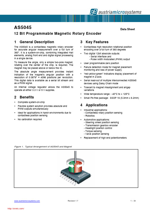
1 General DescriptionThe AS5045 is a contactless magnetic rotary encoder for accurate angular measurement over a full turn of 360°. It is a system-on-chip, combining integrated Hall elements, analog front end and digital signal processing in a single device.To measure the angle, only a simple two-pole magnet, rotating over the center of the chip, is required. The magnet may be placed above or below the IC.The absolute angle measurement provides instant indication of the magnet’s angular position with a resolution of 0.0879° = 4096 positions per revolution. This digital data is available as a serial bit stream and as a PWM signal.An internal voltage regulator allows the AS5045 to operate at either 3.3 V or 5 V supplies.2 BenefitsComplete system-on-chipFlexible system solution provides absolute andPWM outputs simultaneously Ideal for applications in harsh environments due tocontactless position sensing No calibration required3 Key FeaturesContactless high resolution rotational positionencoding over a full turn of 360 degrees Two digital 12bit absolute outputs:- Serial interface and- Pulse width modulated (PWM) output User programmable zero positionFailure detection mode for magnet placementmonitoring and loss of power supply “red-yellow-green” indicators display placement ofmagnet in Z-axis Serial read-out of multiple interconnected AS5045devices using Daisy Chain mode Tolerant to magnet misalignment and airgapvariations Wide temperature range: - 40°C to + 125°CSmall Pb-free package: SSOP 16 (5.3mm x 6.2mm)4 ApplicationsIndustrial applications:- Contactless rotary position sensing - Robotics Automotive applications:- Steering wheel position sensing - Transmission gearbox encoder - Headlight position control - Torque sensing- Valve position sensing Replacement of high end potentiometersFigure 1. Typical Arrangement of AS5045 and MagnetAS504512 Bit Programmable Magnetic Rotary Encoder Data SheetTable of Contents1General Description (1)2Benefits (1)3Key Features (1)4Applications (1)5Pinout (4)5.1Pin Configuration (4)5.2Pin Description (4)6Electrical Characteristics (5)6.1AS5045 Differences to AS5040 (5)6.2Absolute Maximum Ratings (non operating) (6)6.3Operating Conditions (6)6.4DC Characteristics for Digital Inputs and Outputs (7)6.4.1CMOS Schmitt-Trigger Inputs: CLK, CSn. (CSn = internal Pull-up) (7)6.4.2CMOS / Program Input: Prog (7)6.4.3CMOS Output Open Drain: MagINCn, MagDECn (7)6.4.4CMOS Output: PWM (7)6.4.5Tristate CMOS Output: DO (8)6.5Magnetic Input Specification (8)6.6Electrical System Specifications (9)6.7Timing Characteristics (10)6.7.1Synchronous Serial Interface (SSI) (10)6.7.2Pulse Width Modulation Output (11)6.8Programming Conditions (11)7Functional Description (12)8Mode Input Pin (13)8.1Synchronous Serial Interface (SSI) (13)8.1.1Data Content (14)8.1.2Z-axis Range Indication (Push Button Feature, Red/Yellow/Green Indicator) (14)8.2Daisy Chain Mode (15)9Pulse Width Modulation (PWM) Output (16)9.1Changing the PWM Frequency (17)10Analog Output (17)11Programming the AS5045 (18)11.1Zero Position Programming (18)11.2Repeated OTP Programming (18)11.3Non-permanent Programming (19)11.4Analog Readback Mode (20)12Alignment Mode (21)13 3.3V / 5V Operation (22)14Choosing the Proper Magnet (23)14.1Physical Placement of the Magnet (24)15Simulation Modeling (25)16Failure Diagnostics (26)16.1Magnetic Field Strength Diagnosis (26)16.2Power Supply Failure Detection (26)17Angular Output Tolerances (26)17.1Accuracy (26)17.2Transition Noise (28)17.3High Speed Operation (28)17.3.1Sampling Rate (28)17.4Propagation Delays (29)17.4.1Angular Error Caused by Propagation Delay (29)17.5Internal Timing Tolerance (29)17.6Temperature (30)17.6.1Magnetic Temperature Coefficient (30)17.7Accuracy over Temperature (30)17.7.1Timing Tolerance over Temperature (30)18Package Drawings and Markings (31)19Ordering Information (31)20Recommended PCB Footprint (32)5 Pinout5.1 Pin ConfigurationFigure 2. Pin Configuration SSOP165.2 Pin DescriptionTable 1 shows the description of each pin of the standard SSOP16 package (Shrink Small Outline Package, 16 leads, body size: 5.3mm x 6.2mmm; see Figure 2).Pins 7, 15 and 16 supply pins, pins 3, 4, 5, 6, 13 and 14 are for internal use and must not be connected.Pins 1 and 2 MagINCn and MagDECn are the magnetic field change indicators (magnetic field strength increase or decrease through variation of the distance between the magnet and the device). These outputs can be used to detect the valid magnetic field range. Furthermore those indicators can also be used for contact-less push-button functionality.Pin 6 Mode allows switching between filtered (slow) and unfiltered (fast mode). This pin must be tied to VSS or VDD5V, and must not be switched after power up. See chapter 8 Mode Input Pin.Pin 8 Prog is used to program the zero-position into the OTP (see chapter 11.1 Zero Position Programming).This pin is also used as digital input to shift serial data through the device in Daisy Chain configuration, (see chapter 8.2 Daisy Chain Mode).Pin 11 Chip Select (CSn; active low) selects a device within a network of AS5045 encoders and initiates serial data transfer. A logic high at CSn puts the data output pin (DO) to tri-state and terminates serial data transfer. This pin is also used for alignment mode (Figure 14) and programming mode (Figure 10).Pin 12 PWM allows a single wire output of the 10-bit absolute position value. The value is encoded into a pulse width modulated signal with 1µs pulse width per step (1µs to 4096µs over a full turn). By using an external low pass filter, the digital PWM signal is converted into an analog voltage, making a direct replacement of potentiometers possible.Table 1. Pin DescriptionPin Symbol Type Description1MagINCn DO_OD Magnet Field Mag nitude INC rease; active low, indicates a distance reduction between the magnet and the device surface. See Table 52MagDECn DO_OD Magnet Field Mag nitude DEC rease; active low, indicates a distance increase between the device and the magnet. See Table 53 NC - Must be left unconnected4 NC - Must be left unconnectedPin Symbol Type Description 5 NC - Must be left unconnected6Mode - Select between slow (low, VSS) and fast (high, VDD5V) mode. Internal pull-down resistor.7 VSS S Negative Supply Voltage (GND)8Prog_DI DI_PD OTP Prog ramming Input and Data Input for Daisy Chain mode. Internal pull-down resistor (~74kΩ). Connect to VSS if not used9 DO DO_TD ata O utput of Synchronous Serial Interface10 CLK DI,ST Cl oc k Input of Synchronous Serial Interface; Schmitt-Trigger input11 CSn DI_PU,STC hip S elect, active low; Schmitt-Trigger input, internal pull-up resistor (~50kΩ)12 PWM DO P ulse W idth M odulation of approx. 244Hz; 1µs/step (opt. 122Hz; 2µs/step)13 NC - Must be left unconnected14 NC - Must be left unconnected15VDD3V3 S 3V-Regulator Output, internally regulated from VDD5V. Connect to VDD5V for 3V supply voltage. Do not load externally.16 VDD5V S Positive Supply Voltage, 3.0 to 5.5 VDO_OD digital output open drain S supply pinDO digital output DI digital inputDI_PD digital input pull-down DO_T digital output /tri-stateDI_PU digital input pull-up ST Schmitt-Trigger input6 Electrical Characteristics6.1 AS5045 Differences to AS5040All parameters are according to AS5040 datasheet except for the parameters shown below: Building Block AS5045 AS5040Resolution 12bits, 0.088°/step. 10bit, 0.35°/stepData length Read: 18bits(12bits data + 6 bits status)OTP write: 18 bits(12bits zero position + 6 bits mode selection) Read: 16bits(10bits data + 6 bits status)OTP write: 16 bits(10bits zero position + 6 bits mode selection)Incremental encoder Not usedPin 3: not usedPin 4:not usedQuadrature, step/direction and BLDC motorcommutation modesPin 3:incremental output A_LSB_UPin 4:incremental output B_DIR_VPins 1 and 2 MagINCn, MagDECn: same feature asAS5040, additional OTP option for red-yellow-green magnetic range MagINCn, MagDECn indicate in-range or out-of-range magnetic field plus movement of magnet in z-axisPin 6 MODE pin, switch between fast and slowmodePin 6:Index outputPin 12 PWM output: frequency selectable by OTP:1µs / step, 4096 steps per revolution,f=244Hz 2µs/ step, 4096 steps perrevolution, f=122Hz PWM output:1µs / step, 1024 steps per revolution, 976Hz PWM frequencySampling frequency Selectable by MODE input pin:2.5kHz, 10kHzFixed at 10kHz @10bit resolutionBuilding Block AS5045AS5040 Propagation delay 384µs (slow mode) 96µs (fast mode)48µs Transition noise (rms; 1sigma) 0.03 degrees max. (slow mode) 0.06 degrees max. (fast mode)0.12 degreesOTP programming options Zero position, rotational direction, PWMdisable, 2 Magnetic Field indicator modes, 2 PWM frequenciesZero position, rotational direction, incremental modes, index bit width6.2 Absolute Maximum Ratings (non operating)Stresses beyond those listed under “Absolute Maximum Ratings“ may cause permanent damage to the device. These are stress ratings only. Functional operation of the device at these or any other conditions beyond those indicated under “Operating Conditions” is not implied. Exposure to absolute maximum rating conditions for extended periods may affect device reliability. ParameterSymbol Min Max Unit Note DC supply voltage at pin VDD5V VDD5V -0.3 7 V DC supply voltage at pin VDD3V3 VDD3V35VInput pin voltageV in -0.3VDD5V+0.3 V Except VDD3V3 Input current (latchup immunity) I scr -100 100 mA Norm: JEDEC 78Electrostatic discharge ESD ± 2 kV Norm: MIL 883 E method 3015 Storage temperature T strg-55125°CMin – 67°F ; Max +257°FBody temperature (Lead-free package)T Body 260°C t=20 to 40s,Norm: IPC/JEDEC J-Std-020 Lead finish 100% Sn “matte tin” Humidity non-condensing H585%6.3 Operating ConditionsParameterSymbol Min Typ Max UnitNoteAmbient temperature T amb -40125 °C -40°F…+257°FSupply currentI supp 1621 mA Supply voltage at pin VDD5V Voltage regulator output voltage at pin VDD3V3VDD5V VDD3V3 4.53.0 5.03.3 5.5 3.6 V 5V operationSupply voltage at pin VDD5V Supply voltage at pin VDD3V3 VDD5V VDD3V33.03.03.33.33.6 3.6V3.3V operation(pin VDD5V and VDD3V3 connected)6.4 DC Characteristics for Digital Inputs and Outputs6.4.1 CMOS Schmitt-Trigger Inputs: CLK, CSn. (CSn = internal Pull-up)(operating conditions: T amb = -40 to +125°C, VDD5V = 3.0-3.6V (3V operation) VDD5V = 4.5-5.5V (5V operation) unless otherwise noted) ParameterSymbol Min Max Unit NoteHigh level input voltage V IH 0.7 * VDD5VV Normal operation Low level input voltage V IL0.3 * VDD5VVSchmitt Trigger hysteresis V Ion- V Ioff 1V-1 1 CLK only Input leakage current Pull-up low level input current I LEAK I iL-30 -100µA µA CSn only, VDD5V: 5.0V6.4.2 CMOS / Program Input: Prog(operating conditions: T amb = -40 to +125°C, VDD5V = 3.0-3.6V (3V operation) VDD5V = 4.5-5.5V (5V operation)unless otherwise noted) ParameterSymbol Min Max Unit Note High level input voltage VIH 0.7 * VDD5VVDD5VVHigh level input voltage VPROG See Programming ConditionsV During programming Low level input voltage VIL 0.3 * VDD5VVHigh level input current IiL30100µAVDD5V: 5.5V6.4.3 CMOS Output Open Drain: MagINCn, MagDECn(operating conditions: T amb = -40 to +125°C, VDD5V = 3.0-3.6V (3V operation) VDD5V = 4.5-5.5V (5V operation)unless otherwise noted) ParameterSymbolMinMax UnitNote Low level output voltage V OL VSS+0.4 V Output currentI O4 2mAVDD5V: 4.5V VDD5V: 3VOpen drain leakage current I OZ 1 µA6.4.4 CMOS Output: PWM(operating conditions: T amb = -40 to +125°C, VDD5V = 3.0-3.6V (3V operation) VDD5V = 4.5-5.5V (5V operation)unless otherwise noted) ParameterSymbolMinMax UnitNoteHigh level output voltage V OH VDD5V-0.5 V Low level output voltage V OL VSS+0.4 V Output current I O4 2mA mAVDD5V: 4.5V VDD5V: 3V6.4.5 Tristate CMOS Output: DO(operating conditions: T amb = -40 to +125°C, VDD5V = 3.0-3.6V (3V operation) VDD5V = 4.5-5.5V (5V operation) unless otherwise noted) ParameterSymbolMinMax UnitNoteHigh level output voltage V OH VDD5V –0.5VLow level output voltage V OL VSS+0.4 VOutput currentI O4 2mAmAVDD5V: 4.5V VDD5V: 3VTri-state leakage current I OZ 1 µA6.5 Magnetic Input Specification(operating conditions: T amb = -40 to +125°C, VDD5V = 3.0-3.6V (3V operation) VDD5V = 4.5-5.5V (5V operation)unless otherwise noted)Two-pole cylindrical diametrically magnetised source: ParameterSymbolMinTypMaxUnitNoteDiameter d mag 4 6 mm Thickness t mag 2.5 mm Recommended magnet: Ø 6mm x 2.5mm forcylindrical magnets Magnetic input fieldamplitude B pk 4575 mTRequired vertical component of the magnetic field strength on the die’s surface, measured along a concentric circle with a radius of 1.1mm Magnetic offset B off ± 10mT Constant magnetic stray field Field non-linearity5 %Including offset gradient2.44146 rpm @ 4096 positions/rev.; fast modeInput frequency (rotational speed of magnet)f mag_abs0.61Hz36.6rpm @ 4096 positions/rev.; slow mode Displacement radiusDisp0.25mmMax. offset between defined device center and magnet axis (see Figure 18) Eccentricity Ecc 100µm Eccentricity of magnet center to rotational axis-0.12NdFeB (Neodymium Iron Boron) Recommended magnetmaterial andtemperature drift -0.035%/KSmCo (Samarium Cobalt)6.6 Electrical System Specifications(operating conditions: T amb = -40 to +125°C, VDD5V = 3.0~3.6V (3V operation) VDD5V = 4.5~5.5V (5V operation) unless otherwise noted) ParameterSymbolMinTypMaxUnitNoteResolution RES 12 bit 0.088 deg Integral non-linearity (optimum)INL opt± 0.5 deg Maximum error with respect to the best line fit. Centered magnet without calibration, T amb =25 °C. Integral non-linearity (optimum)INL temp± 0.9 degMaximum error with respect to the best line fit. Centered magnetwithout calibration, T amb = -40 to +125°CIntegral non-linearity INL ± 1.4 degBest line fit =(Err max – Err min ) / 2Over displacement tolerance with 6mm diameter magnet, without calibration,T amb = -40 to +125°C Differential non-linearity DNL ±0.044 deg 12bit, no missing codes 0.06 1 sigma, fast mode (MODE = 1)Transition noiseTN0.03deg RMS1 sigma, slow mode (MODE=0 or open)Power-on reset thresholds On voltage; 300mV typ. hysteresisOff voltage; 300mV typ. hysteresisV on V off 1.37 1.08 2.2 1.9 2.9 2.6VDC supply voltage 3.3V (VDD3V3)DC supply voltage 3.3V (VDD3V3)20Fast mode (Mode = 1); until status bit OCF = 1Power-up timet PwrUp80msSlow mode (Mode = 0 or open); until OCF = 196Fast mode (MODE=1)System propagation delay absolute output : delay of ADC, DSP and absolute interfacet delay384µsSlow mode (MODE=0 or open) 2.48 2.61 2.74T amb = 25°C, slow mode (MODE=0 or open)Internal sampling rate for absolute output:f S2.35 2.61 2.87 kHzT amb = -40 to +125°C, slow mode (MODE=0 or open) 9.90 10.42 10.94T amb = 25°C, fast mode (MODE = 1)Internal sampling rate forabsolute outputf S9.38 10.42 11.46kHz T amb = -40 to +125°C, : fast mode (MODE = 1)Read-out frequency CLK1MHz Max. clock frequency to read out serial dataFigure 3. Integral and Differential Non-linearity (example)Integral Non-Linearity (INL) is the maximum deviation between actual position and indicated position. Differential Non-Linearity (DNL) is the maximum deviation of the step length from one position to the next. Transition Noise (TN) is the repeatability of an indicated position6.7 Timing Characteristics6.7.1Synchronous Serial Interface (SSI)(operating conditions: T amb = -40 to +125°C, VDD5V = 3.0~3.6V (3V operation) VDD5V = 4.5~5.5V (5V operation) unless otherwise noted) ParameterSymbol MinTypMaxUnitNoteData output activated (logic high)t DO active 100 nsTime between falling edge of CSn and dataoutput activated First data shifted to output registert CLK FE500 nsTime between falling edge of CSn and firstfalling edge of CLKStart of data output T CLK / 2 500nsRising edge of CLK shifts out one bit at a timeData output valid t DO valid357 375 394 nsTime between rising edge of CLK and dataoutput validData output tristate t DO tristate100 nsAfter the last bit DO changes back to“tristate”Pulse width of CSn t CSn 500ns CSn = high; To initiate read-out of next angular position Read-out frequencyf CLK>01MHzClock frequency to read out serial data分销商库存信息:AMSAS5045-ASST AS5045-ASSU AS5045 PB AS5045 DB V2AS5045 AB。
The introduction of our SP502 transceiver paved the way for a new generation of multi-mode transceivers that are being designed into next generation networking products. The SP504multi-mode transceiver is the latest member of the family and offers: reduced external V.35termination; V.36 & EIA-530A modes; and receiver tri-state and fail-safe ability.As with the SP502 and SP503, the SP504 can be programmed via software to the different avail-able physical protocols and is also drop-in com-patible with its predecessors.The versatility of the SP504 is ideal for multi-protocol applications such as Frame Relay sys-tems, X.25 routers/switches and multi-protocolrouters. These multi-protocol systems will usu-ally contain multiple ports to accommodate the different interfaces. The SP504 can support all the ports through software and provide conve-nient DTE or DCE functionality to the port. DTE and DCE configuration is provided on the next page and also in the SP504 data sheet.The designer can evaluate the SP504 with our SP504Evaluation Board . This evaluation board basically allows the user to access the pins directly through probe points on the board.The designer can also access the device by software through the three serial port connec-tors on the board. Details on the evaluation board can be found in the SP504 data sheet.SP504Application NoteSP504 - DTE/DCE Configuration Many systems may require the serial port to be configured as either a DTE or DCE. The SP504 is an ideal candidate for a space saving DTE/ DCE solution.To perform this with the SP504, the driver out-puts of the first SP504 are connected back into the receiver inputs of the second SP504, and vice versa. The common input/output lines can be routed to the connector and be used as ei-ther driver outputs or receiver inputs. Refer to the following page for configuration details. When the two SP504 devices are connected as such, one device must be disabled while the other is transmitting and receiving data. Dis-abling one of the SP504 devices allows the other to communicate over the serial bus. One is dedicated to a DTE configuration to the se-rial port and the other is a dedicated DCE de-vice. Disabling the DTE device implies that the serial port will be configured as a DCE, and vice versa.Disabling the SP504 drivers are important be-cause a bus contention problem can occur if two drivers are active at the same time. The drivers of the nonactive SP504 must be tri-stated by writing "0000" into the driver decoder(TDECX ) lines when the I/O lines are used asinputs into the receivers. The receivers do not have to be tri-stated but should be configured so that the receiver input impedance is rela-tively high (≥12kΩ) such as RS-422 or RS-485. The receiver inputs will not affect the signals on the driver outputs if the input impedance isat least 12kΩ. If the RDECX is configured with"0000", the input impedance defaults to at least 12kΩ.Please note that most of the V.35 termination resistors are internal to the SP504. As such, the driver output impedance during tri-state is approximately 20kΩ. This should not affect or degrade the incoming driver signal from the other end. Refer to the waveform graphs in the next few pages. The "DTE" waveforms cap-ture the driver and receiver signals at the serial port containing the two SP504 devices. The "DCE" waveforms are measured in the SP504 at the other end. For example, the TxD driver output on the DCE side corresponds to the RxD receiver on the DTE side (side containing two SP504 devices). Similarly, the TxC driver out-put on the DTE side should be the same as the RxC receiver input on the DCE side.Even though the signal is not degraded, the lower impedance basically adds the driver out-put impedance (20kΩ) and the receiver input impedance in parallel. When the active SP504 is configured to RS-232 mode, the typical re-ceiver input impedance is 5kΩ which will yield 4kΩ. When in the other modes except V.35, the typical input impedance is 15kΩ which yields 7.5kΩ when the receivers are configured in differential mode (i.e. RS-422, RS-449, V.36, etc.) which is still greater than the 4kΩ mini-mum requirement for RS-422 and RS-423. The input impedance for the V.35 receiver is typi-cally 100Ω. The driver tri-state impedance will decrease the input approximately 0.5Ω to 1Ωgiven that the external 150Ω termination resis-tor is switched off or disconnected from the non-inverting driver output of the disabled SP504. This configuration will allow the proper data communications between DTE and DCE. How-ever for NET1/NET2 certification testing, the driver outputs must be physically disconnected from the receiver inputs. The common I/O paths will interfere with various impedance and cur-rent testing for the driver or receiver in V.28, V.11 and V.35 modes.元器件交易网The tri-state enable and disable timing must be considered. Given two systems, each config-ured in DTE/DCE operation, containing two SP504’s each, System 1 is the DTE, and System 2 is the DCE. Assume System 1 is now configured to a DCE and System 2 is config-ured to a DTE; the two SP504 devices within each system will have to switch states. If System 1 switches to DCE before System 2 tri-states its driver, the bus will share driver outputs until System 2 switches to DTE, thus causing bus contention problems. In both systems, the active SP504 should be tri-stated first before enabling the tri-stated SP504. Al-though the bus contention will not damage the SP504 devices, it should be avoided to prevent short circuit currents at the driver outputs. One last consideration for DTE/DCE hookup is the charge pump capacitors. Many have in-quired about sharing the 22µF caps. For a mini-mal requirement, the C1 and C2 capacitors must be separate for each SP504 device. Although this can be functionally done, Sipex does not recommend this practice. Please be aware that if one SP504 becomes nonfunctional, it can affect the other SP504 as well.Waveform for TxD Input © Output; DCE, RS-422 mode @ 10MbpsWaveform for RxD Input ©Output; DCE, RS-422 mode @ 10Mbps Waveform for TxD Input © Output; DTE, RS-422 mode @ 10MbpsWaveform for RxD Input © Output; DTE, RS-422 mode @ 10MbpsDRIVER INPUTDRIVER OUTPUTDRIVER INPUTDRIVER OUTPUTDRIVER INPUT DRIVER OUTPUT DRIVER INPUTDRIVER OUTPUTWaveform for TxD Input © Output; DCE, V.35 mode @ 10MbpsWaveform for RxD Input © Output; DCE, V.35 mode @ 10Mbps Waveform for TxD Input © Output; DTE, V.35 mode @ 10MbpsWaveform for RxD Input ©Output; DTE, V.35 mode @ 10MbpsDRIVER INPUTDRIVER OUTPUTDRIVER INPUTDRIVER OUTPUTDRIVER INPUTDRIVER OUTPUTDRIVER INPUTDRIVER OUTPUTSP504 - Switching the 150Ω V .35 Termination ResistorThe SP504 requires one 150Ω resistor to ground on each non-inverting (b) driver output. The 150Ω resistor to ground is necessary to comply with the V.35 short circuit impedance of 150Ω±15Ω. The resistors will need to be switched out when V .35 mode is not active. To perform this, the designer can use one of two methods: add a relay or switch in series with the resistor or implant the resistors inside the V .35cable.Adding the resistors to the cable is relatively easy. In DTE mode, two drivers are usually ac-tive, therefore you will only need two resistors.The 150Ω resistors can be connected individu-ally from pin S (data) to signal ground (pin B)and pin W (clock) to signal ground (pin B) of the V .35 ISO-2593 connector.For DCE applications, an additional driver may be used for a secondary clock signal. If a cable is used on the DCE end, a conversion or "mini"cable is necessary to insert the resistors and route the proper signals to the DTE cable. The resis-tors can be connected from pin S (data), pin W (clock) and an unassigned pin (2nd clock) to sig-nal ground, pin B. Of course the pins on the"mini" cable will have to be routed to the appro-priate end on the DTE V .35 cable. (ie. pin S, pin W and the unassigned pin will be routed to pin T, pin X and pin AA, respectively, on the DTE end.)Another method is to include the 150Ω resistors on the printed circuit board with the SP504 add-ing switches or relays. This method may be pre-ferred if a common connector/cable (ie.DB-25) is used for V .35 and some other mode.The switches must have low on-resistance, pref-erably less than 1Ω. NMOS FETs can be used as configured on the opposite page. The gate of the NMOS device is connected to pin 18 of the SP504. This pin is HIGH when the SP504 is in V .35 mode and goes LOW in all other modes.Pin 18 is not described in the data sheet for the SP504 but can be used to control the switching of the FETs or relays.Sipex recommends Siliconix's LITTLE FOOT™MOSFET devices such as the Si9959DY™ Dual N-Channel Enhancement-Mode MOSFET. The r DS(on) is typically less than 0.3Ω and the devices are in 8-pin SOIC packages.™ - LITTLE FOOT is a trademark of Siliconix, member of TEMIC Group.元器件交易网Termination Resistor Implementation on PC Board.SP504AN SP504 Application Note © Copyright 2000 Sipex Corporation 11ORDERING INFORMATIONModel Temperature Range Package Types SP504CF ...............................................0°C to +70°C .............................80–pin JEDEC (BE-2 Outline) QFP 元器件交易网。